Note: Descriptions are shown in the official language in which they were submitted.
3 1~ ~
MICROWAVE PACKAGE HAVING
A MICROWAVE FIELD MODIFIER OF DISCRETE
ELECTRICALLY CONDUCTIV ELEMNTS
DISPOSED THEREON
TECHNICAL FIELD
The invention pertains to cartons, packages, cookware and the
like for use in microwave heating, cooking, and baking; and more
specifically to such cartons, ~ackages and cookware incorporating
microwave field modifiers which are useful for such thinys as
generating high surface heat on adjacent food matter to effect
browning and/or crispening; or for balancing surface heating an~ deep
microwave heating of underlying food product; or for partially
protecting underlying or adjacent food matter from direct exposure to
microwave energy to obviate overcooking and/or overheating the food
matter; or for simply effecting a more uniform microwave energy
field.
BACKGROUND OF THE_INVENTION
Microwave ovens possess the ability to heat, cook or bake i~ems,
particularly foodstuffs, extrem~ly rapidly. Unfortunately, microwave
heating also has its disadvantages. For example, microwave heating
alone in today's microwave ovens often fails to achieve such
desirable results as evenness, uniformity, browning, crispening, and
reproducibility. Contemporary approaches to achieving these and
~O other desirable results with microwave ovens include the use of
microwave field modiFying devices such as microwave susceptors and/or
microwave shields. Such devices have been incorporated in microwave
packages; which herein includes wrapping materials, cartons,
containers, cookware and the like.
Microwave susceptors and reflectors, like other materia1s and
constructions have some degree of microwave reflectance (R),
absorbance (A) and transmittance (T); or collectively RAT properties.
RAT properties are measured in terms of percentage of microwave
energy reflected by (R), absorbed by (A), and transmitted through (T)
.
:, , . . ;
: . ~ . ~ ;
, .. ~ . ~
2 ~L,~83~
a material or construction. Thus1 the aggregate of the R, A and T
values will total 100%.
~ enerically, a microwave shield is relatively opaque to
microwave energy. In terms of RAT, a shield will have a relatively
low T value. Microwave shields are exemplified by such highly
electrically conductive materials as aluminum foil. Although
shields are generally though~ of as non-heating elements, a shield
could also be a susceptor, i.e., heat appreciably, and visa-versa.
Thus, a shield is an element with relatively low T regardless of its
tendency to yenerate heat.
Generically, microwave susceptors are devices which, when
disposed in a microwave energy field such as exists in a microwave
oven, respond by generating a siynificant amount of heat. The
susceptor absorbs a portion of the microwave energy and converts it
direc~ly to heat which is useful, for example, to crispen or brown
foodstuffs. Thus, microwave susceptors generally have a relatively
high microwave absorbance (A) value. In addition to high absorbance,
susceptors include a mechanism to convert the absorbed microwave
energy to heat. For e~ample, heat may result from microwave induced,
intramolecular or intermolecular action; or from induced electrical
currents which resul~ in so called I-squared-R losses in electrically
conductive devices; or from dielectric heating of dielectric
material disposed between electrically conductive particles, elements
or areas which type of heating is hereinafter alternatively referred
to as fringe field heating or capacitive heating.
As noted, microwave susceptors and reflectors, and other
materials and constructions, have an effect on the microwave power
distribution within a microwave oven. Tha~ is, they interact with
the microwave energy within the oven through their RAT properties and
cause the microwave energy field to be modified. Accordingly,
devices and constructions which act to modify the microwave field or
microwave energy power distribution within a microwave oven are
referred to herein collectively as microwave field modifiers.
The patent literature is replete with a variety of teachings
with respect to the US2 of materials and constructions for use in
microwave ovens as microwave heaters (e.g , susceptors) and
reflectors. For instance, Uni~ed States Patent 4,230,924 which
3 ~ 3 ~ ~
issued October 28, 1980 to William A. Brastad et al discloses a
Method And Material For Prepackaging Food To Achieve Microwave
Browning. Such material may be a dielectric wrapping sheet having a
flexible metallic coating thereon such as aluminum, in the form of a
relatively thin film or relatively thick foil, the coating being
subdivided into a number of individual metallic islands or pads
separated by criss-crossing non-metallic gaps provided by exposed
dielectric strips on the wrapping sheet. An orthogonal pattern o~
square such metallic islands is shown; and ranges of island sizes and
island spacing are stated.
In the thin film embodiments of Brastad et al, there is a
balancing of m~crowave heating within the thin metallic coatings
(i.e.~ current heating in thin, vapor deposited metallic coatings),
and the degree of microwave transparency which enables direct
microwave heating of, for example, a food enclosed within sueh a
wrapping sheet. In the relatively thick foil embodiments, there is a
balancing o~ microwave induced heating in the dielectric substrate
strips disposed between the microwave reflective, foil covered
islands (i.e., fringe field heating), and the degree of microwave
transparency of the sheet through the uncovered dielectric strips.
United States Patent 4,883,936 which issued November 28, 1989 to
Maynard et al discloses Control Of Microwave Interastive Heating By
Pa~terned Deact~vation. This deals with deactivating portions of
thin film susceptors as a way of making susceptors having patterned
active areas. ---
United States Patent 4,864,089 which issued September 5, 1989 toTighe discloses Localized Microwave Radiation Heating through the use
of coating medium: it states that conversion efficiency can be
controlled by the choice and amount of conductive and semi-
3Q conductive ~aterials in the medium.
United States Patent 4,~66,232 which issùed September 12, 1989to James L. Stone discloses a Food Package For Use In A Microwave
Oven which, it states, may comprise depositions of metalized ink on
areas of a container where enhanced heat is desired, and/or
depositions of metalized ink on areas of a container to provide
microwave protection. Stone states, without supporting data, that
.~ .
.
4 2~3~`
such ink deposits may be of the same or different thicknesses and
densities to effect different degrees of heating and shielding.
United States Patent 4,904,836 ~hich issued February 27, 1990 to
Turpin et al discloses a Microwave Heater And Method 0F Manufacture
5 wherein heating is effected in microwave lossy coating material
having specified ranges of inverse penetration depths; and wherein
coatings are provided which may comprise areas of lesser or greater
depth than other area of the coating of lossy material.
European Patent App1ication 0 345 523 which was filed May 23,
1989 discloses a microwave susceptor having a plurality of regions
where a$ least one region has an altered microwave responsiveness
which is achieved by disruptions in the susceptor surface.
While some of ~he problems associated with achieving desired
heating, cooking, and baking results in microwave ovens have been
solved to some extent by others, they have not been solved in the
same manner or to the same exten~ as is provided by the present
invention.
SUMMARY QF THE INVENTION
In one aspect of the present invention a microwaveable package
is provided which includes a top wall, a bottom wall, and a side wall
encompassing and connecting the top wall to the bo~tom wall to form
an enclosure. The side wall has a microwave field modifier attached
thereto or integral therewith to form a substantially continuous
vertically disposed annular shield.
z5 In a second aspect of the present inven~ion a microwaveable
package is provided which includes a first wall and a first microwave
field modifier. The microwave field modifier includes an
electrically conductive microwave active coating material pattern
coated on a predeter~ined zone of the wall to define an array of
electrically conductive discrete elements.
In a third aspect of the present invention a microwaveable
package is provided which includes a top wall, a bottom wall, and a
side wall encompassing and connecting the top wall to the bottom wall
to form an enclosure. The side wall has a microwave field modi~ier
attached thereto or integral therewith to form a substantially
continuous vertically disposed annular shield. The microwave field
modifier includes an electrically conductive microwave active coating
, : :
2 ~ $ ~
material pattern disposed on a predetermined zone of the wall to
define an array of electrically conductive discrete elements.
BRIEF_DESCRIPTION OF THE DRAWINGS
While the specification concludes with claims which particularly
point out and distinctly claim the subject matter regarded as forming
the present invention, it is believed the invention will be better
understood from the following description taken in conjunction with
the accompanying drawings in which identical features or elements are
identically designated in the several views, and in which:
Figure l is a plan view of a discrete microwave field modifier
which may be placed in or attached ~o or made integrally with package
embodiments of the present invention;
Figure 2 is an enlarged fragmentary plan view of the microwave
field modif;er shown in Figure l;
Figure 3 is an enlarged fragmentary plan view of an alternate
microwave field modifier which may be incorporated in~o embodiments
of the present invention;
Figure 4 is a plan view of another alternate microwave field
modifier which may be incorporated into embodiments of the present
invention;
Figure 5 is a plan view of another alternative embodiment of a
microwave field modifier;
Figure 6 is an enlarged fragmen~ary plan view of the alternate
microwave field modifier shown in Figure 5;
Figure 7 is a perspective view of a package of the present
invention haviny an integral cover and in the open position and
having an array of comestible bakeable articles disposed therein;
Figure 8 is a fragmentary sectional view taken along section
line 8-8 of Figure 7;
Figure 9 is a perspective view of the package of Figure 6
without the comestible bakeable ar~icles disposed therein and with a
side wall peeled back to better show the microwave field modifier
disposed thereon;
Flgure lO is a top plan view of a blank which may be erected to
form the package of Figure 7;
- : :.
: . :
., ~ .
.
.,' ' ~ ~
6 ~ 3 ~ ~
Figure 11 is a perspective view similar to Figure 9 of a second
preferred package of the present invention;
Figure 12 is a ~op plan view similar to Figure 10 which may be
erected to form the package of Figure 11;
5Figure 13 is a perspective view similar to Figure 9 of a third
preferred package of the present invention;
Figure 14 is a perspective view similar to Figure 6 of a fourth
preferred package of the present invention including separate top and
bottom parts; and
10Figure 15 is a top plan view of a blank which may be erected to
form either the top or bottom par~ of the package of Figure 14.
DESCRIPTION OF THE INYENTION
Briefly, the present invention provides microwaveable packages
which comprise one or more microwave field modifiers. The preferred
microwave field modifiers (an example of which is indicated generally
as 20 in Figure 1) basically include a substrate 22 and an array
for~ed from a plurality of discrete electrically conductive elements
24 disposed thereon. The discrete electrically conductive elements
24 are preferably formed from pattern coating a coating material to
areas of the substrate 22; and even more preferably by printing. The
elements 24 preferably have an elongate portion and/or preferably are
staggered relative to each other side to side.
Generally, (and therefore without specific reference numbers) as
used herein, elongate has its ordinary meaning: i.e., having a form
notably long in comparison to its width. Additionally, the elongate
elemen~s described herein are preferably substantially straight
albeit it is not intended to thereby exclude serpentine, wavy, and
curved shapes. Also, the elongate elements pre~erably have radiused
ends as shown to lessen the propensity for electrical arcing.
30Staggered relation, as used herein, is intended to include but
not be limited to shapes such as elongate, square, and rectangular
elements which are in side by side relation but which have their ends
offset from one another. The offset need not be necessarily uniform
throughout the array.
35The microwave field modifier of the present invention may be a
discrete unit covering an entire substrate or only a portion thereof.
Likewise, several modifiers having varying effects can be located in
~': : ',
- . : . ~ .
:~ . . .
~ . ,
7 ~ 3 ~ ~
different zones on the same substrate. A modifier may consist o~
layered arrays. For example, an array can be disposed on both
surfaces (sides) of a substrate. Alternatively, a modifier, or
modifiers, may be integrated into selected portions of packages which
herein includes wrapping materials, cartons, containers, cookware and
the like.
Additionally, the modifier can be a layered or laminated
structure comprising, for instance, one or more additional layers for
such purposes as strength, arc suppression, and interactive modifier
functions. For example, albeit not depicted in the figures, a
ther~oplastic or thermosetting coating or film may be applied to the
modifier structure to cover the electrically conductive coating
material to preclude direct contac~ between the electrically
conductive coating material and an adjacent load such as a quantity
of food product; and to pro~ect the modifier from electrical arcing
in the event the modifier is placed in close proximity to
electrically conductive artic~es. Furthermore, such a layered
construction can be made by pattern coating a thermoplastic film with
electrically conductive coating material, and then laminating the
pattern coated film to paper or car~onboard or some other dielectric
substrate.
The discrete electrically conductive elements are preferably
formed by pattern coating a coating material onto the substrate.
Among the advantages of this structure are significant cost and
equipment savings relative to current thin f~lm susceptors. It is
even more preferable if the coating material is applied to the
substrate by printing and most preferably by rotogravure printing.
Printing offers advantages such as cost and efficiency savings over
other coating processes and rotogravure printing equipment is
generally currently available to carton manufacturers.
The coating material of the present invention general1y includes
a binder material system, which comprehends a resin and a solvent,
and electrically conductive particles. In addition the coating
material may include various other components.
The binder system is used to bind the electrically conductive
particles together in contasting rela~ion. The binder system also
preferably functions to bind the coating material to the dielectric
, ~ .
, ' . ' ' ~ ' `:
' ' .
.
8 ~ 3 ~ ~
substrate. Included in a binder system is a resin and a solvent.
Exemplary preferred resin materials include nitrocellulose, ethyl
cellulose~ polyvinylbutyral, polyvinylpyrrolidone, poly (methyl vinyl
ether/maleic acid) co-polymer resins and acrylics. A nitrocellulose
can be purchased from General Printing, Ink Division, Sun Chemical
Corporation, Cleveland, Ohio as a 40% solu-tion of 18-25 CPS RS
nitrocellulose. (This solution includes 17% isopropyl alcohol, 23%
ethyl acetate and 20% n-propyl acetate by weight.) An ethyl
cellulose can be purchased from Hercules Inc., Wilmington Delaware as
Ethyl Cellulose N-4. A poly ~methyl vinyl ether/maleic acid)
co-polymer resin can be purchased from the GAF Corporat;on of Wayne,
New Jersey under the trade name~Gantrez~. Gantrez~ is a registered
trademark of the GAF Corporation. Gantre~ currently comes in three
basic forms; Gantrez~ AN, Gantrez~ ~S and Gantrez~ S. Gantre~
ES-~25 is preferred. A polyvinylbutyral can be purchased from
Hoechst-Celanese of Somerville, NJ under the trade name Mowital~. It
is available in several molecular weights. The preferred types are
coded B-20H, B-30H and B-~OT by Hoechst-Celanese. Mowatol~ is a
registered trademark of Hoechst-Celanese. Polyvinylpyrrolidone may
be obtained from GAF Corporation, Wayne, New Jersey and Sigma
Chemicals of St. Louis, Missouri.
Electrically conductive particles which may be used to make
coating materials include pure metallic particles, some metallic
o~ides, metal alloy particles, carbon particles and graphite
particles. Furthermore, the conductive particles preferably have
irregular shapes; even more preferably are also relatively flat; and
most preferably are also of differing shapes and sizes; all of which
promote electrical contact between the elements.
A preferred conductive particle which has been found successful
is Nickel Flake HCA-1 which may be purchased from the Novamet
Company, Wyckoff, N.J. The Novamet Nickel Flake HCA-1 is a dendritic
particle formed of spheroids which have been connected together and
flattened. Thus, a preferred conduct;ve particle has a flattened
dendritic shape. A second preferred particle may be purchased from
Cabot Corporation, Waltham, Mass as Carbon Black Regal~ 99R. This
particle is also relatively flat and has a size of about .36
nanometers.
~ -
2~3~
Some other components which may be used as constituents of
coating materials include binder solvents, emulsifying agents, acids
and liquid materials which will chemically unite with the other
constituents of the coating material to cause the coating material to
solidify after being applied in a fluidized state. In applications
of coating materials which require some flexibility, the coating
materials may further comprise plasticizer material. Additionally,
anti-settling agents or other constituents may be included in coating
material formulations.
Additionally, an undercoating placed on the substrate prior to
printing increases conductivity. Likewise, an overcoating placed
over the elements increases con~uctivity. Conductivity is further
increased by using both an undercoating and an overcoating. If
binder of the undercoating and/or overcoating uses the same solvent
as the binder of the coating material conductivity is increased even
further. Consequently, an undercoating or overcoating is used, more
preferably an undercoating and an overcoating is used, even more
preferably an undercoating or overcoating uses the same solvent as
the coating material and most preferably an undercoating and
overcoating uses the same solvent as the binder of the coating
material.
Furthermore, increasing the acidity of the binder seems to have
a beneficial effect on conductivity. The more acidic the binder the
greater the conductivity. Thus, it may be beneficial to add acidic
binder additives to the coating material, such as acid complex
forming additives. While not intending to be bound it is believed
the surface chemistry effects of adsorption may be providing this
benefit. The adsorption may allow for closer contact of the metal
particles with each other giving rise to better conductivity. A1SQ~
it is possible salts are being formed with the oxide making the metal
more free for electrical conduction.
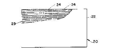
Figure 1 illustrates an exemplary microwave field modifier,
indicated generally as 20, which embodies the present invention. The
substrate 22 of Figure 1 is twenty point cartonboard such as is
3S commonly converted into such things as cartons for packaging
microwaveable food products: i.e., packages which are suitable for
being placed in a microwave oven to heat, cook or bake the contents
, . , -
~, . .
of the package without removing the contents from the carton. Other
exemplary substrate 22 materials include carton~oard, coated
cartonboard, thermoplastic film, thermoplastic nonwovens, thermoset
plastics, or ceramic.
Disposed on the substrate 22 is an array formed from a plurality
of discrete electrically conductive elements 24. In Figure 1, the
array e~tends over the entire top surface 28 of the substrate 22
except for a perimetric zone 29 which is devoid of coating material
26. The perimetric zone 29 acts to insulate the edges of modifier 20
so as to substantially obviate arcing between the electrically
conductive elements 24 and any metallic material disposed adjacent
the modifier 20. Furthermore, although the array of Figure 1 extends
over the entire surface of the substrate 22, the modifier may be
limited to one or more zones of the substrate 22.
Referring no~l to the enlarged fragmentary view of Figure 2, the
preferred modifier 20 of Figure l includes elements 24 which are
uniform in size and shape except at some row ends, and have lenyths L
and widths W, respectively. Thus, the array preferably substantially
comprises elements 24 which are uniformly configured. Additionally,
the elements 24 are preferably linearly aligned in straight rows
parallel to each other. The rows are linearly spaced apart by a
distance designated SL; and side by side rows are spaced widthwise a
distance designated SW. Further, the rows are in staggered relation
so that side by side adjacent elements are linearly offset by a
distance designated OS. The degree of stagger, in percent, of such
an array is (OS/L)(100).
Referring to Figure 3, an alternative embodiment of a microwave
field modifier 120 of the present invention is illustrated wherein
the elongate elements 124 have a generally serpentine shape. The
length L of any element 124 is along its center line. But for the
shape of the elements 124, and the degree of stagger, modifier 120 is
substantially similar in construction to modifier 20 of Figure 1.
Accordingly, substrate 122 can be the same dielectric material as
substrate 22 of Figure 1, or can be of different dielectric material.
The elements 12~ may be different in size and/or shapei and the
elements 124 may comprise the same or different coating material
~e.g., coating material having a different surface resistivity). As
,
.
~: .
shown, in this array, the elements 124 of adjacent rows are staggered
about 50% percent.
The modifier 120 of Figure 3 is more isotropic than the modifier
20 of Figure 1. In other words, the effectiveness of the array as a
shield is less dependant upon the orientation of the array relative
to an incoming microwave. ~f the R values are plotted against the
degree of rotation throughout 360 using the RAT test described
hereinafter a sinusidal-type curve will result. For the modifier 20
of Figure 1, the maximum R would be relatively high and this portion
f the curve would be relatively broad. In addition~ the low R
portion of the curve would be relatively narrow. For the modifier
120 of Figure 3, the curve would have generally the same shape,
however, the maximum R would be less and the low R portion of the
curve would be narrower, while the high R portion of the curve would
be wider. Thus, a modifier 120 which is more isotropic than a second
modifier 20 may provide better shielding in a microwave oven even
though its maximum R value is 1ess since within the microwave oven
the waves come in at all angles.
The modifier 20 of Figure 1, however, can be made more isotropic
by layering the array (as by printing both sides of a single
substrate) such that the elements ~4 in one layer are substantially
perpendicular (i.e., so that the high R range for one will shield
waves coming in at an angle o-f low R for the other) to the elements
24 of the other layer. An example of this can be seen in Figure 7
which will be discussed hereinafter. This -provides an isotropic
modifier of even higher R than the modifier 120 of Figure 3.
Referring to a second alternate embodiment seen in Figure 4,
discrete microwave field modifier 220 includes a dielectric substrate
222 on which a staggered array of square elements ~24 are disposed,
and which has an uncoated perimetric zone 229. But for the shape of
the elements 224, and the degree of stagger, modifier 220 is
substantially similar in construction to mod;fier 20 of Figure 1.
Accordingly, substrate 222 can be the same dielectric material as
substrate 22 of Figure 1, or can be o~ different dielectric material.
or different in size and/or shape; and the elements 224 may comprise
the same or different coating material (e.g., coating material having
a different surface resistivity). Albeit elements 224 are shown to
, . ,, :
, ,
12 ~ 3~
have unradiused corners, it is not intended to thereby preclude
square and rectangular elements from having radiused corners.
As shown, in this array, the elements 224 of adjacent rows are
staggered about fifty (50) percent. Being staggered, the modifier
220 of square elements 224 are both more effective as shields and as
susceptors, i.e., heaters, than squares which are orthogonally
aligned.
In addition, the modifier 220 of Figure 4 is more isotropic than
the modifier 20 of Figure 1 and the modifier 120 of Figure 3.
Consequently, the modifier 220 of Figure 4 will also have a lower
maximum R than either of the previous embodiments.
Turning now to Figure 5 ~and Figure 6, another alternate
microwave field modifier 320 is shown to comprise an array of Y-shape
elements 324 on a dielectric substrate 322. Figure 4 is a
fragmentary, enlarged scale view of modifier 320. The Y-shape
elements 324 have three elongate portions, and are disposed in side
by side, vertically extending rows. The length L of the elongate
portion in this embodiment is the maximum path along the center line.
In this embodiment the three possible paths are identical in length.
In the rows of this embodiment, the stems of the Y-shape elements 324
are partially nested between the arms of adjacent Y-shape elements
324. Also, the arms of the Y-shape elements 324 in adjacent rows are
partially sideways nested between the arms of adjacent Y-shape
elements 324; and some of the arms of sideways nested Y-shape
25 elements 324 are in parallel relation. Fringe field heating can be
varied in such an array by varying the spacing between portions of
adjacent Y-shape elements 324, as well as the the size of the Y-shape
elements 324, the width of their elongate portions, and the
dielectric loss property of the substrate 322 material. This
modifier 320, as compared to modifiers 20 similar to Figure 1, are
more isotopic; i.e., their RAT properties are less sensitive to
positional variances when such modifiers 320 are placed in microwave
ovens, and have lower maximum R values.
As previously described a shield is relatively opaque to
35 microwaves. In other words, a shield has a relatively low T value.
Thus, a shield preferably has a T value of less than about 40%, more
preferably less than about 10% and most preferably less than about
13 ~ 3~
5%. Due to their low T values, shields also generally have high R
values. Shields are particularly useful for such purposes as
preventing overheating in certain areas, i.e., at corners and edges,
and generally slowing down microwave cooking.
S Any modifier can be characterized by its microwave reflectance,
absorbance, and transmittance values: i.e., its RAT values.
However, since shields are characterized in terms of RAT, and
particularly R and T, RAT values are particularly helpful with regard
to determining shielding ability.
One method of measuring RAT values uses the following Hewlett
Packard equipment: a Model 8616A Signal generator; a Model 8743A
Reflection-Transmission Test Unit; a Model 841lA Harmonic Frequency
Converter; a Model HP-84108 Network Analyzer; a Model 8418A Auxiliary
Display Holder; a Model 8414A Polar Display Unit; a Model 8413A Phase
Gain Indicator; a Model S920 Low Power Wave Guide Termination; and
two S281A Coaxial Waveguide Adapters. In addition a digital
millivolt meter is used.
Connect the RF calibrated power output of the 8616A Signal
Generator to the RF input of the 8743A Reflection-~ransmission Test
Unit. The 8411A Harmonic Frequency Converter plugs into the 8743A
Reflection-Transmission Test Unit's cabinet and the 8410B Network
Analyzer. Connect the test channel out, reference channel out, and
test phase outputs of the 8410B ~etwork Analyzer the test amplitude,
reference and test phase inputs, respectively, of the 8418A Auxiliary
Display Holder. The 8418A Auxiliary Display Holder has a cabinet
connection to the 8414A Polar Display Unit. The 8413A Phase Gain
Indicator has a cabinet connection to the 8410B Network Analyzer.
The amplitude output and phase output of the 8413 Phase Gain
Indicator is connected to the digital millivolt meter's inputs.
The settings of the 8616A Signal Generator are as follows:
Frequency is set at 2.450GHz; the RF switch is on; the ALC switch is
on to stabilize the signal; Zero the DBM meter using the ALC
calibration output knob; and set the attenuation for an operating
range of 11db. Set the frequency range of the 8410B Network Analy~er
to 2.5 which should put the reference channel level meter in the
"operate" range. Set the amplitude gain knob and amplitude vernier
'
.. . ~ ,. ....
14 21~3~
knob as appropriate to zero the voltage meter readings for reflection
and transmission measurements respectivelY.
Microwave field modifier samples are three and one-half inches
in diameter.
For Reflection place the 8743A reflection-Transmission Unit in
the reflection mode A S281 Coaxial Waveguide Adaptor is connected
to the "Unknown" port of the 8743A Reflection-Transmission Test Unit.
A perfect shield (aluminum foil) is placed flat between the
reflection side of the S281 wave guide adaptor and the S290A Low
Power Guide Termination. The amplitude voltage is set to zero using
the amplitude gain and vernier knobs of the 8410B Network Analyzer.
The shield is replaced by the sample of the microwave field modifier.
In other words the sample is placed between the S281A Coaxial
Waveguide Adaptor and the S920A Low Power Waveguide Termination and
the attenuation voltage is measured. Normally, four readings are
taken per sample and averaged. The samples are rotated clockwise
ninety degrees per measurement. After the second measurement the
sample is turned over (top to bottom) for the final two measurements.
For polarized, isotropic samples care must be taken to orient the
samples such that the maximum and minimum readings are obtained. The
R value is the maximum reading. These samples may also be rotated in
increments other than ninety degrees.
For Transmission place the 8743A Reflection-Transmission Unit in
the transmission mode. A 10db attenuator is placed in the
transmission side of the line, between the l'In'l port of the 8743
Reflection-Transmission Unit and a second S281A Coaxial-Waveguide
Adaptor. The two SZ81A Coaxial-Waveguide Adaptors are aligned and
held together securely. The amplitude signal voltage is zeroed using
the amplitude gain and vernier knobs of the 8410B Network Analyzer.
The modifier to be tested is placed between the two waveguide
adaptors and the attenuation voltage is measured. Four readings are
taken as described above for the reflection measurement. Reflection
and transmission values should be calculated in the same manner; i.e.
average or maximum.
Absorption is calculated by subtracting the transmission
measurement and the reflection measurement from 1.00.
:, ,
It should be noted that RAT values as measured in the Network
Analyzer may be different from actual RAT values when a microwave
field modifier is placed in competition with a food load. The food
and the microwave field modifier compete for the available microwave
energy. The competition can be analogized to a circuit consisting of
a generator connected to two impedance loads in parallel. The
generator represents the magnetron while one impedance load
represents the food load and the other impedance load represents the
microwave field modifier. The network analyzer procedure above does
not include the food load resistor. Thus, when the food load is
added to the circuit its "impedance" relative to the microwave field
modifier's resistance is not known. If the food load's "impedance"
is significantly less than the modifier's "impedance" most of the
microwave energy will ~low through the food. Consequently, design of
lS modifier's inevitably involves some trial and error based upon the
actual food to be heated.
As previously described, a susceptor is a microwave field
modifier which absorbs microwave energy and heats appreciably when
exposed to a microwave field. One method for determining the ability
of a modifier to heat (at least relative to other microwave field
modifiers) is the Energy Competition Test described below. Using a
carousel microwave oven which has a power rating of 30 BTU/min as
measured with a 1000 gram water load an effective susceptor
preferably has a AT at two minutes of about 90F or more, more
preferably about 150F or more, and most preferably about 20~F or
more~
To conduct the Energy Competition Test, place a 150 ml pyrex
beaker containing 100 grams of distilled water in a microwave oven on
a carousel along with a three and three quarter inch diameter pyrex
petri dish containing 30 grams of Crisco~ Oil. These items are
placed side by side about nine inches on center apart. Take an
initial temperature reading of the oil. Subject these items to the
full power of the microwave field for a total of two (~) minutes; at
30 second intervals open the microwave oven and stir the oil with a
thermocouple measuring and recording the temperature. This
measurement should be taken as quickly as possible to minimize
cooling of the oil. This procedure provides a control.
. , .
,
3 ~ ~
16
Repeat the above procedure with a three and one half inch
diameter sample of a microwave field modifier submerged in the oil.
8egin with the oil at about the same initial temperature as with the
control. It may be necessary to place an inert weight, such as a
glass rod, on top of the modifier to keep it submerged in the oil.
The data can be normali7ed by adjusting the initial temperature to a
standard 70F by subtracting or adding the initial temperature
deviation from 70F to each of the temperatures recorded.
Once the test has been run and, one method which can be used for
comparison of various microwave field modifiers is to compare the
change in temperature over the two minute time interim. Thus, the
two minute ~T is calculated by subtracting the two minute ~T of the
oil alone from the two minute ~T of the oil and susceptor.
Additionally, the two minute ~T of the susceptor is normalized by
adding or subtracting any initial temperature variance of the oil
from 70F.
As with measuring RAT through the use of a network analyzer, the
Energy Competition Test may not predict exactly how well a modifier
will heat in the microwave in conjunction with a food load. However,
the use o-f water is intended to simulate the modifier in competition
with a load. The greater the variance in microwave properties of the
actual food -load from the properties of the water load, the less
accurate this test will be. Consequently, it may be desirable to use
another amount of water or competing load in a particular application
comparing possible microwave field modifiers to reduce the amount of
trial and error necessary to achieve the desired results with the
actual food load. In any event some trial and error will inevitably
be necessary.
Despite the above, a microwave field modifier of the present
invention may be tailored with minimal trial and error to provide
desired RAT values and heating characteristics by selectively
altering certain variables. Thus, a modifier can be designed having
a wide range of shielding and heating properties. Some of these
variables relate to the array, i.e., the element shape, size,
orientation and arrangement relative other elements; some to the
coating material; and lastly, some to the substrate or possible
overcoatings or undercoatings. Generally speaking, the
. ..; ~
- , - ...
3 ~ ~
17
directionality of the various variables, with respect to tailoring
;ts RAT properties will be discussed below with reference to Figure
2. The directionality, however, applies to all embodiments o~ the
present invention.
Included among the array variables are the lengths, widths,
spacing, and the degree of stagger between adjacent elements 24. One
variable is the length L of the element 24. In genera,, the maximum
length L of the element 24 is preferably less than about 4 cm and
even more preferably less than about 3 cm. In addition the length L
is preferably one-half (1/2) cm or greater and most preferably one
(1) cm or greater. In any case, L should be less than the amount
that would induce electrical ~arcing. In this general range
increasing length L increases microwave reflectance, and decreases
both microwave absorbance and transmittance of the modifier 20.
Additionally, increasing the length L of the elements 24 increases
the magnitude of the alternating voltage and current which is induced
in the elements 24, and thus will tend to increase the tendency for
arcing to occur across the end to end gaps between adjacent elements
24 and overheating within the elements 24.
With regard to width W, a width of from abvut 0.001 inches to
about 1.0 inches is preferred; with a width W from about 0.010 inches
to about 0.10 being more preferred. In this general range increasing
width W decreases microwave reflectance, and increases the wavelengtn
bandwidth response of the modifier 20 which makes the modifier 20
less sensitive to wavelength changes which can be induced by such
things as contact with a food load. Additionally, the elongate
elements 24 preferably have a L/W ratio of from about 2:1 to about
200:1; and even more preferably from about 10:1 to about 40:1.
End to end spacing SL is preferably from about 0.010 inches to
about 0.100 inches and in this range increasing end to end spacing
spacing SL or side to side spacing SW decreases microwave
reflectance, increases both microwave absorbance and transmittance of
the modifier 20, and decreases the fringe field heating of the
intervening portions of dielectric substrate 22.
Side to side spacing SW is pre~erably from about 0.010 inches to
about 0.10 inches. Increasing side spacing SW in this range
decreases both fringe field heating and shielding.
.
. , . ~ , .
: ` '
18 2~ 3~
The degree of stagger is preferably about 30% or 3~% for maximum
shielding and heating for highly conductive coating materials.
Included among the coating material variables are the
resistivity, shape and size of the conductive particles; and the
dielectric properties (i.e., the dielectric constants, loss factors,
and dielectric strengths) and surface electrical conductivity of the
dried coating material. The surface electrical conductivity of the
conductive elements 24 is relatively high as measured in terms of
surface resistivity: preferably one-hundred (100) ohms per square or
less; more preferably ten (10) ohms per square or less; Still more
preferably three (3) ohms per square or less; even more preferably
one (1) ohm per square or less; and most preferably one-tenth (0.1)
ohm per square or less. Increasing surface electrical conductivity
of the elements 24 in this range directly increases microwave
reflectance, and decreases microwave transmittance of the modifier
20.
Achieving a dried coating having conductivity in the desired
ranges identified above is aided by certain features. For example,
putting down a sufficient quantity of coating material is important.
The more coatin9 material, i.e., the thicker the coating materialt
the more conductive. Coating material thickness is preferably from
about 0.0001 inches to about 0.003 inches and even more preferably
from about 0.0005 inches to about 0.002 inches.
Also, viscosity of the coating material can be important
depending upon the coating process used. The viscosity of the
coating material is preferably from about S0 cps to about 7000 cps.
For rotogravure printing the viscosity is preferably from about 100
cps to about 175 cps as measured with a ~3 zahn cup. In any event
the viscosity should be such that the coating material is suitable
for the chosen coating process used; be it pain~ing, spraying,
printing~ silkscreen printing or rotogravure printing. Achieving the
desired viscosity may require the addition of resin, solvents or
other additives after the initial mixing of the coating material as
is commonly done in printing processes.
Additionally, an undercoating placed on the substrate prior
to printing increases conductivity. Likewise, an overcoating placed
over the elements increases conductivity. Conductivity is further
.- ~ ~ . :
': , , ' `" .
., ~
: ..... . . . .
:
2~83~
19
increased by using both an undercoating and an overcoating. If
binder of the undercoating and/or overcoating uses the same solvent
as the binder of the coating material conductivity is increased even
further. Consequently~ an undercoating or overcoating is used, more
preferably an undercoating and an overcoating is used, even more
preferably an undercoating or overcoating uses the same solvent as
the coating material and most preferably an undercoating and
overcoating uses the same solvent as the binder of the coating
material. Additionally, an overcoating of Gantrez~ AN or Gantrez~ S
for example, may be useful to provide an FDA approved barrier.
Furthermore, increasing the acidity of the binder seems to
have a beneficial effect on conductivity. The more acidic the binder
the greater the conductivity. Thus, it may be beneficial to add
acidic binder additives to the coating material, such as acid complex
forming additives. While not intending to be bound it is beli~ved
the surface chemistry effects of adsorption may be providing this
benefit. The adsorption may allow for closer contact of the metal
particles with each other yiving rise to better conductivity. Also,
it is possible salts are being formed with the oxide mak.ing the metal
more free for electrical conduction.
With respect to the conductive particles of the coating material
of elements 24 the electrically conductive particles are preferably
less than twenty-five microns in size (i~e., their maximum
dimensions); and more preferably less than ten microns in size.
Finer particles result in greater coating co~ductivity for a given
weight percent of the particles in a given coating material. Also, a
mix of different particle sizes acts to increase surface electrical
conductivity for a given weight percent of the particles in a given
coating material. Particle aspect ratio --i.e., the ratio of the
longest dimension to the shortest dimension of a particle-- is also
important. A high aspect ratio (i.e., greater than ten to one) is
preferred because it promotes electrical contact between the
particles in solidified coating materials, and such conductive
particles are more susceptible to microwave heating than particles of
smaller aspect ratios. Additionally, particles of higher resistivity
will act to decrease surface conductivity of coating materials; and
particles having jagged shapes and edges ~end to promote electrical
20~1336~
contact between conductive particles in a coating material, and will
thus tend to increase the surface conductance of the elements 24.
With regard to the dielectric properties of the dried binder and
other fluids a high dielectric loss factor will act to increase
dielectric heating (i.e., capacitive heating within the conductive
element 24 between conductive particles); a high dielectric strength
reduces the tendency to arc; and a high dielectric constant will
increase microwave reflectivity and power handling ability.
Included among the remaining variables are the dielectric
properties (i.e., the dielectric constants, loss factors, and
dielectric strengths) of the substrate 22 and any optional
overcoating material. With respect to the substrate 22, a high
dielectric constant will function to increase microwave reflectance
and power handling capacity; a high dielectric loss factor will act
to increase dielectric heating; and high dielectric strength prevents
breakdown at higher induced voltages~ Thus, high dielectric strength
reduces the tendency to arc, and thus tends to obviate arc charring
of the substrate 22. This protects the modifier 20 from breakdown
inasmuch as carbon particles which result from arcing would tend to
short circuit the elements across the intervening gaps. The same is
true with respect to any optional overcoating or undercoating which
may be applied to separate the modifier from direct contact with the
food.
The above directionality information with respect to the various
variables is generally true. However, there is a complex
relationship among the various variables. Due to this complex
relationship, manipulation of a particular variable while keeping the
remaining variables constant can have a minimal effect in a
particular situation; i.e., with a particular coating material and
pattern. In contrast, manipulation of the same variable may have a
truly significant impact in a second situation.
While not wishing to limit the invention, one possible method of
designing a microwave field modifier of the present invention having
desired RAT properties follows. Pick a coating material which will
have the desired conductivity range when dried (see above) and a
suitable substrate. Determine the maximum line length that can be
used without arcing. This is done by coating a series of lines
': , ' ;, .'
., ,,., .: ~ ,
2~ 6~
having differing lengths up to about 4 cm and preferably about 1 mm
wide onto the chosen substrate. Place these lines in the microwave
field along with 100 gms of water in a beaker (to simulate a food
load).
Choose a line length approximately 20% less than the minimum
line length that arcs. Coat an array pattern with this line length
L, lmm wide W, gaps of lmm between the ends SL and the sides SW of
the lines and a 25% offset between adjacent rows of lines.
Determine the performance characteristics of the array. The
modifier may be tested in a network analyzer to determine the RAT.
Also perform an energy competition tPst to determine the heating
ability. Alternatively, this array can be tested in conjunction with
an actual food load to determine its performance characteristics.
To increase heating and shielding, increase the line length and
decrease the size of the gaps. Changing to a more conductive coating
material or depositing a thicker coating (which increases
conductivity) will also increase heating and shielding. If there is
excessive heating and a reduction in shielding is tolerable adjust
oppositely.
If this array simply produces too much heating for the shielding
required then change the dielectrics in the coating material,
substrate and any overcoatings or undercoatings to lower loss
materials and possibly change to a more cnnductive coating material.
Another possible way to increase shielding is to increase the amount
Of the offset. The above method and list of adjustable variables is
not intended to be all-inclusive but illustrates how adjustment to
desired RAT values might be made.
As stated above, the relative RAT values of microwave field
modifiers of present invention may be tailored to meet specific needs
of variaus foodstuffs by selectively varying such parameters as the
surface electrical conductance or resistance of the elements; the
lengths, widths, spacing, and the degree of stagger between adjacent
elements; the resistivity, shape, size, and aspect ratio of the
conductive particles; and the dielectric properties (~.e., the
dielectric constants, loss factors, and dielectric strengths) of the
substrate and/or the dielectric binder.
22
To illustrate the versatility of the microwave field modifiers
of the present invention three exemplary embodiments will be
presented: one with high shielding properties and low heating
properties; one with high shielding properties and high heating
properties; and one with low shielding properties and high heating
properties.
_ample 1
An exemplary microwave field modifier of the present invention
having relatively high shield;ng properties and relatively low
heating properties can be described with reference to Figures 1 and
2. The array is silk screen printed onto twenty point cartonboard
using a 109 mesh, 0.0032 inch diameter monofilament polyester
silkscreen. The coating material is comprised of about sixty percent
by weight of silver particles, and manifest a dried surface
resistivity of less than one-half (0.5) ohm per square. Such a
coating material ca~ be purchased from Acheson Colloids Company, A
Division Of Acheson Industries, Inc., Port Huron, Michigan, and is
identified as Electrodag 477SS.
Still referring to Figures 1 and 2, the elongate elements 24 are
2 1/2 cm. long, 0.040 inches wide, spaced 0.160 inches end to end,
spaced 0.160 inches side to side, and have stagger (pattern offset)
OS of about 25%. The pattern may be printed with the elongate
elements 24 horizontally on the front side of the substrate 22 and
with the elongate elements 24 oriented vertically on the back side of
the substrate 22.
ExamPle 2
An exemplary microwave modifier of the present invention having
high shtelding properties and substantial heating ability can be
described with respect to Figures 1 and 2. In this example the heat
is primarily generated as a result of fringe field or capacitive
heating between the elements 24 due to the relatively high
conductivity and the dielectric properties of the coating material
components. Some heat, however, is generated by I-squared-R heating
of the elements 24 themselves. The surface resistivity of the dried
coating material is less than about two ohms per square.
The array is silk screen printed onto twenty point car~onboard
substrate 22 using a 109 mesh, 0.0032 inch diameter monofilament
-
, ;:; '
;
2~36~
23
polyester silkscreen. The coating material used is forty-seven
percent (47%) copper and ~ifty-three percent (53%) acrylic binder
system coating material which may be purchased from Acheson Colloids
Company, Port Huron, Michigan as Acheson copper Electrodag ~437.
The array might have an appearance similar to that illustrated
in Figures 1 and 2. The elongate elements 24 are two (2.0)
centimeters long and 0.032 inches wide. The array has an end gap of
0.045 inches, a side gap of 0.027 inches and and offset of 30%.
Examole 3
An exemplary embodiment having low shielding and substantial
heating ability can be described with reference to Figure 4. In this
example the heat is primarilj generated in the elements 224
themselves due to the relatively low conductivity of the elements 224
and the dielectric properties of the coating material components.
The array is pattern coated onto a twenty point cartonboard
substrate 222 using a 109 mesh, 0.0032 inch diameter polyester
monofilament or a similar 18-F multifilament silkscreen. The coating
material is comprised of 60% nickel and 40% nitrocellulose by weight.
The nickel may be purchased from the Novamet Company of Wyckoff, New
Jersey and is identified as Nickel HCA-1 Flakes. The nitrocellu1Ose
may be purchased from the General Printing Ink Division, Sun Chemical
Corp., Cleveland, Ohio, and is identified as nitrocellulose solution
#266-133.
The array might have an appearance similar to that illustrated
in Figure 4. The elements 224 are seven (-7-) millimeter squares
spaced 0.6 mm apart on all sides. In addition, the elements 224 are
offset 50%.
Additional exemplary embodiments using various binder systems
are provided below:
Example 4
This is an exemplary embodiment using a ten percent solution of
Mowital~ B30H polyvinylbutyral. A ten percent solution can be
obtained by dissolving 5 grams of B30H powder in 45 grams of methanol
(methyl alcohol). To this add 75 grams of Novamet nickel; creating a
60% nickel and 40% (10% solid resin) resin solution. Thus, the final
solution consists of 75 grams nickel and 50 grams of 10% resin
solution.
:,
~, .
3 ~ ~
24
This coating material may then be screen printed in a pattern
similar to that of Figure 1. The dimensions of this pattern may be
as follows: end gap SL of .045 inches, side gap SW 0.275 inches,
length L of ~787 inches, width ~ of .035, and overlap of 31%
Furthermore, if this coating material is screen printed onto a
substrate such as cartonboard which has been pre-coated with a layer
of the polyvinylbutyral solution, (i.e., 10% solution in methanol
without nickel) by using a doctor blade or a mayer rod the
conductivity and the reflectance (R) may be increased.
If the first sample is coated with the same 10% solution such as
to produce an overcoating of the susceptor coatiny, the change in RAT
properties may be similar to those of the second sample which has an
undercoating.
If the sample with the undercoating of polyvinylbutyral is now
15 overcoated to produce a printed sample with nickel which has both an
undercoating and an overcoating, the conductivity and the
reflectivity (R~ may be further increased.
Example 5
This Example uses a twenty percent solution of Gantrez ES-225.
A twenty percent solution can be obtained by starting with 20 grams
of material as supplied (50% resin and 50% ethanol solvent) This
provides 10 grams resin and 10 grams solvent. Add 30 grams of
ethanol solvent to the solution; creating a 20% resin and 80% solvent
solution. This provides 10 grams resin and 40 grams solvent or 50
grams of total solution. To this add 75 grams of Novamet nickel;
creating a 60% nickel and 40% (20% resin) resin solution coating
material. Thus the final solution consists of 75 grams nickel and 50
grams of 20% resin solution.
This solution is then screen printed or rotogravure printed
~with only minor adjust~ents to viscosity) in a pattern similar to
that of Figure 1. The dimensions of this pattern may be as follows:
end gap SL of 0.045 inches; side gap SW of 0.0275 inches; length L of
0.787 inches; width W of 0.035 ;nches; and a stagger of 31%.
ExamPle 6
This example uses a ten percent solution of
polyvinylpyrrolidone. A ten percent solution can be obtained by
dissolving 5 grams of polyvinylpyrrolidone powder in 45 grams of
- . . ~,
,
2~48~
methanol (methyl alcohol). To this add 75 grams of Novamet nickel;
creating a 60% nickel and 40% (10% solid resin) resin solution.
Thus, the final solution consists of 75 grams nickel and 50 grams of
10% resin solution.
This solution may then be screen printed in a pattern similar to
that of Figure 1. The dimensions of this pattern may be as follows:
end gap SL of .045 inches, side gap SW 0.275 inches, length L of .7~7
inches, width W of .035 inches and overlap of 31%.
Exam~le 7
This Example uses a 5.4 percent solution of ethyl cellulose. A
5.4 percent solution can be obtained by starting with 2.2 grams of
ethyl cellulose resin. To this add 0.5 grams of an anti-settling
agent such as Bentone SDZ which is available from National Lead
Chemicals, Hightstown, New Jersey. Add 4.4 grams of a modifier such
as Uni-Rez 7055 (fumaric-acid modified rosin ester binder), available
from Union Camp Corp., Wayne, New Jersey; and 1.8 grams of a
plasticizer such as ~erculon D (hydrogenated methyl ester of rosin),
available from Hercules Chemical Corp, Wilmington, Delaware. Also
add 32.1 grams of n-propyl acetate as a solvent providing a 5.4
percent ethyl cellulose solution. To this add 59 grams of Novamet
nickel HCA-1 flakes; creating a 59% nickel and 41% (5.4% resin) ethyl
cellulose resin solution coating material. Thus the final solution
consists of 59 grams nickel and 41 grams of 5.4% resin solution.
This solution is then screen printed or rotogravure printed
(with only minor adjustments to viscosity) in a pattern similar to
that of Figure 1. The dimensions of this pattern may be as follows:
end gap SL of 0.045 inches; side gap SW of 0.0275 inches; length L of
0.787 inches; width W of 0.035 inches; and a stagger of 31%.
It can be seen from the foregoing examples which include various
combinations of relatively high and relatively low shielding with
relatively high and relatively low heating ability, that modifiers
having virtually any properties can be designed. In the above
examples high shielding is defined as having a transmittance of about
10% or less and high heating is defined as having a ~T at two minutes
of about 125F or greater.
. . ...
.
` ~
:
26 ~ 4
The above described microwave field modifiers of the present
invention can be used for example~ in packages for heating, baking,
cooking, etc..., various food items. Referring to Figures 7 and 8, a
package 30 having microwave field modifiers printed thereon for
baking a cupcake batter product is illustrated. The carton 30
comprises a box-type container portion 31, and an integral cover 32.
The box-type container portion 31 of carton 30 comprehends a bottom
wall 35, side walls 41, 42, 43 and 44, and four glue flaps which are
designated 45. The integral cover 32 of carton 33 comprehends a top
wall 36, side walls 46, 47, and 48, and two glue flaps 49.
The carton 30 has microwave field modifiers located thereon and
is adapted for baking a cupcake batter product 52. The carton 30
includes eight commercially available susceptor cups 54, i.e., paper
cups lined with a thin vapor deposited metallic coating which may be
obtained from IVEX Corporation, Newton, MA, into which the batter 52
is divided. The cups 54 may alternatively include a microwave field
modifier as described above which is designed to heat. These cups 54
are filled with batter 52 and placed in an annular orientation around
a centrally located thermoplastic measuring cup 55. Such a
configuration has been found to be very effective for achieving
uniform baking, rising, and browning of cup cakes.
Referring to Figure 9, the side walls 41, 42, 43, and 44 of the
carton base 31 includes a microwave field modifier 20 similar to
Example 1. The inner surface of the side wall 41, 42, 43, and 44 is
coated with an array of elongate elements 24 running horizontally and
the outer surface of the side wall 41, 42, 43, and 44 has an
identical array of elongate elements 24 oriented vertically. A
portion of side wall 43 is peeled back (and one glue flap re~oved) to
illustrate this arrangement. Such two layer arrays of pattern
elements 24 (ie, on both surfaces of the side ~alls) provide a more
isotopic response to positional differences when such constructions
are disposed in microwave oven fields. This side wall 41, 42, 43 and
44 modifier provides a shield around the sides to slow down baking at
the edges and also to even out the baking.
The top wall 36 of the carton 30 includes a second modifier 220
similar to Figure 3 but for having the elements 224 orthoganally
aligned. The inner surface of the top ~all 36 of the carton 30 is
. .
. - .
~83~
27
coated with an array of generally square elements 224. This modifier
220 may be similar to Example 3. This modifier 220 generates a
significant amount of heat which browns the sur~ace of the cupcakes
and helps qive them the traditional domed top appearance.
The carton 30 may be constructed from the blank illustrated in
Figure 10. The blank shows the modifier 220 which is coated onto the
top wall 36. The blank also shows the side wall 41, 42, 43 and 44
modifier which is coated on the panels 41, 42, 43, and 44, although
the elongate elements 24 coated on the back surface of these panels
41 through 44 is not shown. The printed patterns of coating material
are spaced from the distal and end edges of walls 41 through 44, and
spaced from the edges of top wall 36. Such spacing is to ensure that
adjacent portions of the coated walls are not in contacting relation
in the erected carton 30; and this, in turn, is to ensure that arcing
does not occur in those regions of the carton 30.
Figure 11 is a perspective view of an alternate microwaveable
carton 130 which is substantially like carton 30, Figure 9, except:
carton 130 does not have electrically conductive pattern elements 24
on the outside surfaces of its sidewalls 141, 142, 143 and 144; and
the array of square pattern elements 224 on top wall 136 are in the
staggered relation of Figure 4 rather than being in the orthogonal
array of carton 30, Figure 9. Figure 12 illustrates a blank which
can be erected to form the carton 130 of Figure 11.
Figure 13 is a perspective view of an alternate microwaveable
carton 230 which is substantially identical to-carton 30 but for not
having an array of electrically conductive pattern elements 224 on
the inwardly facing surface of the top wall 236. When such a carton
230 was filled with cup cakes like those shown in Figure 7, the cup
cakes became dome shaped, golden colored, moist, and quite uniform in
their appearance but not quite to the same degree as those in package
30, Figure 11. One advantage to this embodiment is only one side of
the blank needs the coating material coated thereon.
Figure 14 is a plan view of a cut and scored, and pattern coated
cartonboard blank 330B which can be erected to form either the
container section 331 or the cover section 332 of carton 330 of
Figure 15. This view shows the printed patterns of coating material
are spaced from the distal and end edges of walls 3~1 through 34~,
28 2 a ~
and spaced from the edges of top wall 336. Such spacing is to ensure
that adjacent portions of the coated walls are not in contacting
relation in the erected carton; and this, in turn, is to ensure that
arcing does not occur in those regions of the carton 330.
The top 332 is sized, with respect to the bottom 331, so that
the top 332 will fit over the bottom 331. The inside surfaces of the
side walls 341, 342, 343, and 344 of the bottom 331, and the inside
surfaces of s;de walls 346, 347, 348, and 350 of top 332 are provided
with arrays of electrically conductive pattern elements 24 such as
those of carton 30 of Figure 9. Thus, when the to~ 332 covers the
bottom 331, two layers of pattern elements 24 are disposed through
the double side walls of carton ~30. Functionally, it is believed
that the side walls of this construction have about the same
microwave field modifying effect as the side wall portions of carton
30, Figure 9. Although this embodiment is shown without the top wall
modifier as with the embodiment of Figure 13, a top wall modifier
could be added as with the embodiment of Figure 11. Again, an
advantage of this embodiment is the ability to print the coating
material only on one side of the blanks.
While ~articular embodiments of the present invention have been
illustrated and described, it would be obvious to those skilled in
the art that various other changes and modifications can be made
without departing from the spirit and scope of the invention. It is
intended to cover in the appended claims all such changes and
modifications that are within the scope of this invention.
,
. - . . - . . .
' ! , ,