Note: Descriptions are shown in the official language in which they were submitted.
335~
~-Z05264
SUPERCONDUCTI~E ~PTOELECTRONIC ~EVICES WITH
THE BASIC SUBSTANCE Bi2O3
OF SUPERCONDUCTIVE CONJUGATE PHOTOCONDUCTIVIT'f
This invention relates to a number of super-
conductive optoelectronic devices and superconductive
optoelectronic apparatuses with a basic substance Bi2~3
or Bi2O3;M2~ (M-Ca,Sr,Cu) of superconductive-conjugate
05 photoconductivity. The superconductive optoelectronic
devices and apparatuses of the present invention are
novel and vastly different from those of prior art in
that the invention uses a particular combination of the
Bi-based superconductive oxide material and the basic
material Bi2O3 or Bi2O3;M2~ (M=Ca,Sr,Cu) of special
superconductive-conjugate photoconductive character
which reveals photoconductivity below the critical
temperature of the Bi-based superconductive materials
relevant to the basic substance Bi2O3.
The invention also relates to a superconductive
optoelectronic apparatus with Bi2O3 or Bi2O3;M2+ having
a plurality with diversity of the superconductive
optoelectronic devices produced therein in the form of
integrated oircuit at ultra high density, e.g. in two
dimensional array form.
The invention stems from the inventor's
important discovery of a phenomenon that a certain basic
- 2-
33~3~
substance reveals photoconductivity at temperatures
below the critical temperatures of superconductivi~y ~sc
of relevant superconductors, and such photoconductivity
of that basic substance is in a conjugate r~lationship
0~ with the superconductivit~ of the relevant super-
conductors.
In the ensuing description, the "basic
substance" refers to the substance with the above
mentioned character, or that substance which reveals the
superconductive-conjugate photoconductivity to be
defined below. The basic substance to be used in the
present invention is Bi2o3 or Bi2O3;M2+ (M=Ca,Sr,Cu) and
the relevant superconductors are the Bi-based oxides.
Here, we define "Superconductive-Conjugate
16 Photoconductivity" to be a substantially new type of
large photoconductivity in host insulators which emerges
in several steps with decreasing temperature in accord-
ance or correspondence with the critical temperatures of
superconductivity in relevant conductive substances, all
based on the discoveries and inventions disclosed by the
present applicant before. "Photoconductivity" and -
"Superconductivity" are conjugate with each other in
a certain group of systems, such as Bi203 and the
Bi-based oxide superconductors.
With recent development of superconductive
materials, various new superconductive substances have
been found; for instance, superconductive oxide
. - ~ -
~ . - - - . ~
2~ 39~
materials such as those of Y-Ba-Cu-O system and
Bi-Sr-Ca-Cu-O systems. ~owever, most of current
research effort are ~ocusse~ on the raising of
transition temperature or critical current, and not
05 thorough studies except those on the reflection or
scattering have been made on either optical properties
of superconductive substance or industrial applications
of such optical properties. The reason for it is in
thatl generally speaking, researchers have considered
that superconductivity is incompatible with such
physical properties as optical absorption and
photoconductivity and they have assumed that optical
irradiation in the region of an excess amount of energy
with the relevant wave number beyond the energy gap of
1~ the BCS theory will merely destroy the stability of
superconductivity. Further, most of the superconductive
materials which have been developed so far are metals or
alloys or at least metallic, and no superconductive
materials with useful optical properties have been
found. No concept had existed, until the present
inventor dlsclosed the first step, on a new field to be
called "Superconductive Optoelectronics".
on the other hand, if a high-temperature
superconductive o~ide material is combined with
a recently recognized basic materials such as Cu2O or
Bi2O3 of superconductive-conjugate photoconductivity
which reveals its proper photoconductivity at
3~3~
temperatures below the transition temperatures of the
relevant superconductive oxide materials, a number of
new and more efficient electronic devices and
optoelectronic apparatuses may be developed, for
o~ instance, a switching device with no power loss,
an optically operating device with no power loss,
an optically operating logical device, a space parallel
type optically operating apparatus, a camera or an image
forming device possibly with superconducting wiring,
a high-speed optically operating apparatus to be driven
at an extremely low power, and the like.
Although most researchers currently aim at the
raising o~ transition temperatures of superconductive
materials, the inventor has performed a number of
1~ experiments and analyses on optical properties of
superconductive oxide materials, such as those of the
Y-Ba-Cu-O and La-Cu-O system, Bi-Sr-Ca-Cu-O system and
Ba-Pb-Bi-O system and eventually basic substances such
as Cu20 and Bi203. Consequently, the inventor has
discovered an entirely new and remarkable phenomenon in
that some, at least two, of the above basic oxide
substances are superconductive-conjugate
photoconductive-materials to be defined as those which
reveal onsets and steps of photoconductivity at temper-
atures in accordances or correspondences with the
critical temperature for superconductivity (transition
point) of all relevant superconductive materials which
,: ~
'; ' ' ' :, ~' ' '' ,
,
. .
- . .
3~3~
are related to the superconductive-conjugate
photoconductive-materials. The basic su~stances of
superconductive-conjugate photoconductive oxide
materials are so far as electric insulators or
OB semiconductors at room temperature, but when they are
cooled down to the temperatures below the transition
points of the relevant superconductive materials related
to them, they reveal photoconductivity, i.e., they
enhance life time of photocarriers to be observable and
their conductivity varies depending on the intensity of
the excitation light which is incident thereto.
A power-loss-free useful superconductive
optoelectronic device can be formed by combining a basic
substance, e.g., Bi2o3 of superconductive-conjugate
1~ photoconductive-material with its related Bi-based
superconductive material, for instance, the
Bi-Sr-Ca-Cu-O system. What is meant by "superconductive
optoelectronic device with basic substance" is
an optoelectronic device made of a combination of
a superconductive material of one oxide system and
a basic substance of superconductive-conjugate
photoconductive-materials of the same oxide system which
reveals photoconductivity at temperatures below the
critical temperatures of the relevant superconductive
oxide material.
An object of the invention is to provide
a novel superconductive optoelectronic device by using
,:
z~
effectivel~ the optical properties of a "basic
substance~' such as si2o3 or Bi2O3;M2~ (M=Sr,Ca,Cu) of
the superconductive-corljugate photoconductive-materials,
which is newly discovered by the inventor Eor the
06 Bi-based oxide superconductors. Thus, the invention is
neither a mere improvement of the prior art nor
a simpler solution of problems existing in the prior
art, but an entirely new achievement.
A superconductive optoelectronic device
according to the present invention, for instance,
comprises a substrate, a photoconductive gate region
formed on the substrate, and a source region and a drain
region formed on the substrate at opposite sides of the
gate region respectively so as to face toward each other
1~ across the gate region. The source and drain-regions
are made of a superconductive oxide material, while
the gate region is made of a basic substance of
superconductive-conjugate photoconductive-materials
which reveals photoconductivity at temperatures below
ao the critical temperature for superconductivity of the
relevant superconductive materials. The basic substance
of the superconductive-conjugate photoconductive-
material and the superconductive material are of common
origin but with different contents of constituent
elements.
Bias source may be connected across the source
region and the drain region of the optoelectronic
' ' ~.'~ ' '.~'
'
:
~7~
devices of the invention, so as to drive an ele~tric
current through its photoconductive gate region depend-
ing on the intensity of light which is incident to the
photoconductive gate reyion.
0~ Once such a type o~ superconductive opto-
electronic device is formed with a basic substance Bi2O3
or Bi2O3;M2~, it must be naturally straight forward to
develop the new field from such a device to other
devices, and eventually to superconductive opto-
electronic apparatus with a basic substance Bi2O3 or
Bi2O3;M2~, for instance a switching device with no power
loss, an optically operating device with no power loss,
an optically operating logical device, a space parallel
type optically operating device, a camera or an image
1~ forming device possibly with superconducting wiring,
a high-speed optically operating apparatus to be driven
at an extremely low power with highest optical
efficiency, and the like.
For a better understanding of the invention,
reference is made to the accompanying drawings, in
which:
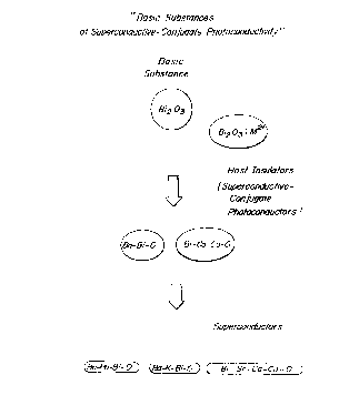
Fig. 1 schematically displays a few inter-
correlations between basic substances or host insulators
and a series of high-T~ superconductors;
2~ Figs. 2a-2c display the temperature dependences
of transient photoconductivity Q(T,A) of (a) the basic
material Bi2o3 (ceramic) at A=660 nm E=4.3 kV/cm~
.
~ 3
(b) the basic material Bi2O3;M2+ (M=Sr, Ca, Cu~ (S213),
single crystal at A=540 nm and E=120 V/cm, and
(c) Bil-Srx-Ca2_x-Cu2-Oz system (x=0), respectively.
All of these are typical examples of the
o~ superconductive-conjugate photoconductivity.
Fig. 2d exemplifies typical dark resistivity p(T) of the
BilSrxCa2_xcu2oz system lx=l);
Figs. 3a, 3b and 3c indicate the wavelength
dependence of the superconductive-conjugate photo-
conductivity Q(T,A) of (a) the basic substance Bi2O3sintered ceramics at T=77 K, E=2.2 kV/cm and (b) the
Bi2O3;M2+ (M=Sr,Ca,Cu), single crystal at T=5.0 K,
E=120 V/cm, and the Bil-Srx-Ca2-x-cu2-oz system (x=0),
respectively;
1~ Fig. 4 is a schematic illustration of the
valence bands and conduction bands of Bi2O3 near the
zone center together with two wavelengths of
photoexcitations at A=547, 570 nm indicated;
Figs. 5a and 5b indicate the basic principle of
technique to detect transient photoconductivity signals
Q(T,A) in insulators with two arrangements of blocking
electrodes;
Fig. 6 exemplifies a block diagram of circuit
arrangement for the transient photoconductivity
2~ measurement for insulators;
Figs. 7(a), (b), (c), (d), and (e) indicate the
X-ray diffraction patterns of (a) Bi2O3 ceramic powder
g
'''','. ~'
. ' ., - ,~
.~''" ~ .
(6N) (monoclinic) and (b) powdered Bi2O3;M2~ (#S213
rhombohedral) and (c) single crystal of Bi2O3,M2+
(#S256), and Fig. 7(d) the Bi2rre3 like crystal structure
and (e) the bonding characters of Bi2Te3 similar to
06 those of Bi2~3;
Fig. 8(a) and 8(b) display spectral responses
of photoconductivity Q(T,A) of (a) sintered sample of
pure Bi2O3 (#B03) at T=77 ~, E=2.2 kV/cm and
(b) Bi2O3;M2~ (#S213 single crystal at T=77 K,
E=320 V/cm);
Fig. 9a exhibits the temperature dependence of
photoconductivity Q(~,A) of single crystal Bi2O3;M
(#S213) at A=540 nm, E=120 V/cm;
Fig. 9b exhibits the magneto-resistance
1~ mobility ~M(T) of ~lectrons and positive holes in
Bi2O3;M2+ (#S213, A=570 nm) as a function of tempera-
ture, both in logarithmic scales, wherein solid lines
illustrate the results o~ fitting of temperature
dependence of ~M(T) in terms of a combination of the
effects of optical and acoustic phonon and neutral
impurity scatterings;
Figs. lO(a), (b) and (c) display the
temperature dependences of superconductive-conjugate
photoconductivity Q(T,A) of (a) the basic material
Bi2O3;M2~ (#S213) at A=540 nm and E=120 V/cm and (b) the
BalPbl_xBixOz system (#S54, x=l, A=520 nm, E=3.6 kV/cm),
respectively together with an example of normal
- 10 -
photoconductivity of Agce in Fig. 10 (a). Fig. 10 (c)
illustrates the temperature dependences of
superconductive-conjugate photoconductivity Q(T,A) of
Balpbl-xBixoz (x=0.4), (#S60) and (x=0.5)(#S135),
OB respectively, at A=580 nm, E=2.2 kV/cm;
Figs. ll(a) and (b) display the wavelength
dependence of superconductive-conjugate photoconduc-
tivity Q(T,A) of the basic substance of Bi203 at
E=2.2 kV/cm, T=77 K and the BalPbl_xBixOz (x=0.5) at
E=2.2 kV/cm, T=4.2 K;
Figs. 12(a) and (b) indicate the phase diagram
of (a) the Bal-Pbl_x-Bix-O~ system and (b) the
Bi2-Sr2-Cal_x-Yx-cu2-oz system in thermal equilibrium in
the dark and also a quasi-phase diagram at
1~ photoexcitation, respectively;
Fig. 13(a) indicates characteristic dependences
of the relative photoresponse on the intensity of
photoexcitation IeX of Bi203;M2+ (#S213 single crystal),
QX/Iexi and the magneto-resistance mobility, ~M, at
T=5.0 K, A=540 nm, E=60 V/cm, H=6.4 KOe;
Fig. 13(b) indlcates a logarithmic replotting
~f (QX/Iex) and ~M of Bi203;M2~ (#S213) in Fig. 13(a) on
the intensity of photoexcitation IeX;
Fig. 14 indicates a logarithmic plotting of the
carrier density (n/Iex) and ~n of Bi2o3;M2+ (#S213) on
the intensity of photoexcitation Ie~ at T=5.0 K,
A=570 nm, E=60 V/cm, ~=6.4 KOe); and
-. .
- , .
~ '
Z~
Fig. 15(a) and (b) indicates a characteristic
plotting of QX/Iex of Bi2O3;M2+ on the IeX at 77 K in
(a) linear scale and (b) logarithmic scale;
Fig. 16 is a schematic sectional view of
o~ a superconductive optoelectronic device according to the
invention;
Fig. 17 is a schematic partial sectional view
of a superconductive optoelectronic alley device
according to the invention;
Figs. 18a and 18b are a diagrammatic
illustration of a space parallel optically operating
superconductive optoelectronic apparatus which uses
alleys of the superconductive optoelectronic devices of
the invention (A) a method of encoding input signals and
1~ (B) a mode of projection by a light source, e.g., LED
array for operation;
Figs. l9(a) and (b) illustrate the concepts of
(a) a "polaron", i.e., a conduction electron or
a positive hole associated with LO-phonons or
ao deformation of host crystal lattice together in free
motion; (b) a "bipolaron" mediated via a coherent
ensemble of phonons or lattice deformations or even
electronic polarization;
Figs. 20(a) and 20(b) illustrate a schematic
form of (a) an exciton with a wavevector K and
transition moment Pl which sometimes couples with
(b) photons with a wavevector ~ and the direction of
. :
~3~ 3
polarization ~;
Fig. 21~a), 21(b) and 21(c) depict
schematically the density of states N(E) as a function
of Energy E for (a) Bi2o3 or Bi2O3;M2+ insulators,
o~ (b) BilSrxCa2_~cu2oz (x=0 insulator) and
(c) Bilsrxca2-xcu2oz (x=l superconductor) respectively;
and
Fig. 22 depicts schemakically the density of
states N(E) as a function of Energy E for the
Bapbl-xBixoz system (a) (x>0.35 insulators), (b) (x~0.3
superconductor), (c) (x~-0.2 superconductor) and
(d) (x<0.15 normal metallic region), respectively.
Throughout different views of the drawing in
Figs. 16-18, l is a substrate, 2 a gate region,
1~ 3 a source region, 4 a drain region, 5 an insulating
layer, 6 a conductive glass layer, 7 an excitation
light, lO an alley-like light source, ll an encoded
image-mask pattern, 12 a correlative image screen, and
13 is a decoding mask optical element alley.
ao The present invention for a superconductive
optoelectronic device uses a particular combination of
the basic material Bi2O3 or Bi2O3;M2+ (M=Sr,Ca,Cu),
a host insulator, of superconductive-conjugate
photoconductive character and the relevant Bi-based
superconductive oxide materials as schematically
enumerated in Fig. l into a form of a device in Fig. 16.
There is a real peculiarity in such a combination.
-13-
' ~ .
3~2
In the inventorls opinion, all of these systems
of high-Tc superconductors have their origins in the
basic substances. For example, the Bal-Bil-Oz specimens
can be synthesized by composing BaCO3 powder with ~i2~3
0~ powders at appropriate sintering temperatures. In the
case of Bi~Ca-Cu-O specimen, one needs additional powder
of CaCO3. By systematically varying the Pb-composition
of the BalPbl_xBixOz, and the Sr-composition of the
BilSrxCa2_xCu2Oz systems, we have also examined and
confirmed the existence of photoconductivity closely
correlated with superconductivity complementary with
each other at least at the conversion boundary, which
we call "superconductive-conjugate photoconductivity".
We have observed even a close correlation of
1~ superconductive-conjugate photoconductivity of the
BilSrxCa2_xCu~Oz system with those of Bi2O3 or Bi2O3;M2+,
the basic substance for all of the Bi-based super-
conductors as illustrated in Figs. 2(a)-(d) and
Figs. lO(a)-(c) and Fig. ll, respectively. The step
temperatures Tps after their onsets in photoconductivity
Q(T,A) of the Ba-Pb-Bi-O system are plotted in Fig. 12a
in accordances or correspondences with the critical
temperatures Tsc in the dark resistivity p(T) as
a functlon of Bi-composition x.
2~ Figs. 3 and 8 display the wavelength
l-dependence of photoconductivity Q(T) of Bi2O3 and
Bi2O3;M2~ in Figs. 2(a) and (b) with the Bilsrxca2-xcu2oz
- 14-
(x=0) in Fig. 2tc). Origins of "the superconductive-
conjugate photoconductivity" and of "real superconduc-
tivity" can be inherently of common characters over the
whole region of x.
0~ Thus, such a combination does have a profound
significance as discussed later. Technically, Bi2O3 can
be a flux for producing the Bi-based high-Tc super-
conductors. This fact guarantees an appropriateness for
materials of the Cate region of a device. Similar is
true of Cu2O for the Cu-based high-Tc superconductors.
Accordingly, we have reexamined yet unexplored
natures of these basic substance such as si2O3 and
Bi2O3;M2+ for the superconductive optoelectronic device
and discovered substantially new natures of these
lB photoconductive materials conjugated with superconduc-
tivity. Here, we describe further details of these
informations below.
The inventor's experiments and analyses on the
photoconductivity of basic substances and superconduc-
tivity of various relevant superconductive materialsshowed that the basic substance and a certain portion of
superconductive materials in their phase diagram reveal
photoconductivity conjugate with superconductivity at
temperature below their regions of transition tempera-
tures of s~perconductivity. For instance, in the case
of superconductive oxides of the Bi-Sr-Ca~Cu-O system,
the inventors discovered that with decreasing Sr content
-15-
,
, ,
.~ '
they exhibit the special feature as if their super-
conductivity can be converted into photoconductivity at
temperatures below their critical temperatures.
Figs. 2 illustrate typical results of
0~ experiments on the photoconductivity of the basic
substance of Bi2O3 and Bi2O3;M2~ with the superconduc-
tivity of the Bil-Srx-Ca2-x-cu2-oz system oxides.
The curve (a) and (b) in Fig. 2 show the temperature
' dependences of photoconductivity of Bi2O3 and Bi2O3;M2~
single crystal which are the basic substances clarified
by the inventor. The curve (c) in Fig. 2 illustrates
the temperature dependence of superconductive-conjugate
photoresponse of Bil-Srx-Ca2_x-Cu2-Oz (x=0) in the dark.
The curve in Fig. 2(d) illustrates the temperature
1~ dependence of electrical resistance of
Bil-Srx-Ca2_x~Cu2-Oz (x=l) in the dark. After a number
of experiments and analyses on Bi2O3, Bi2O3;M2+ and also
the Bi-Sr-Ca-Cu-O system oxides with a general chemical
formula of Bin_y-srx-cam-x-cu2-oz~ the inventors found
28 that Bi203 or Bi203;M2+ exhibit the photoconductivity in
correspondences with the superconductivity of the
Ba-Pb-Bi-O and Bi-Sr-Ca-Cu-O systems. Under the
conditions of
3~ n_ 5, 2~m~ 4, l~y~3, 0~ xS 2, 4~ z~ll,
2~ if the content x of Sr is between 1 and 2, i.e.,
l_ x~ 2j the Bi-Sr-,Ca-Cu-O oxides reveals superconduc-
tivity, while if the content x of Sr is not more than 1,
- 16-
i.e., O~x~l~ the oxides reveals photoconductivity.
More particularly, with n=3, m=2, y=2 under the
above-mentioned conditions, the Bi-Sr-Ca-Cu-O system
reveals superconductivity if r e~g., its content x of Sr
0~ is in the range of 0.7~1~x~2, and if its content x of
Sr is smaller than 0.7~1 such superconductivity
disappears and it revPals complementary photoconduc-
tivity (x=0) at temperature regions below their
transition temperatures. Those materials whose
1~ superconductivity is converted into complementary
photoconductivity and vice versa depending on the
concentration of a part of their ingredient atoms at
temperature regions below their transition temperatures
will be referred to as "superconductive-con~ugate
16 photoconductive materials" and their property will be
referred to as "superconductive-conjugate
photoconductivity" or simply "superconductive
photoconductivity" herein. These are the case even for
Bi2O3 or Bi2O3;M2+. Thus, one may call Bi2O3 or even
Bi2O3;M2+ the basic substances of superconductive-
conjugate photoconductivity for the Bi-based
superconductors.
Curves in Figs. 3(a) to (c) display the
wavelength dependence of photoresponse o~ the basic
substances of the oxide specimen Bi2O3 ceramics at
T~77 K, Bi2O3;M2+ single crystal and Bil-srx-ca2-x-cu2-oz
(x=0) at 4.2 K, respectively. The basic substance Bi2O3
-17-
~. :
ceramics, Bi2O~;M2+ sin~le cr~stal and the oxide
Bil-srx-ca2-x-cu2-oz (x~0) have more or less similar
optical responses in wavelength dependences; more
specifically, as the wavelength A decreases from 650 nm,
o~ their photoresponse Q (T,A) gradually increases, whereas
their photoresponses remain substantially at low levels
for wavelengths longer than 650-700 nm.
The inventors noted that if the basic materials
Bi2O3 revealing photoconductivity at a temperature below
its transition temperature of the Bi-based super-
conductors is combined with another material such as the
Ba-Pb-Bi-O, Ba-K-Bi-O and Bi-Sr-Ca-Cu-O systems reveal-
ing superconductivity at a temperature below its
transition temperature, then such a combination will
1~ provide a useful superconductive optoelectronic device
which reveals both superconductive and photoconductive
characteristics at a temperature below the transition
temperature thereof.
More specifically~ if an optoelectronic element
Of FET-like shape as illustrated in Fig. 16 is formed by
making a gate region with the basic substance Bi2O3 or
Bi~O3;M2+ of superconductive-conjugate photoconductivity
while making a source region and a drain region with
a relevant Bi-based oxide superconductive material,
an output current whose magnitude varies depending on
the wavelength and intensity of light incident to the
gate region can be produced so as to flow across the
- 18-
source and drain regions. If such an optoelectronic
device is sustained at a temperature below the
transition temperature of its superconductive material,
it must work as a superconductive optoelectronic device
o~ which can be used in numerous ways; for instance, as
a power loss-free optical switching device with high-
speed response, an optical detector, an optical signals
amplifying device, or the like.
Under these circumstances, the inventor has
developed an intensive study on the basic substance
Bi2O3 and especially Bi2O3;M2+.
1) Experimental technique
(1) Because the basic material such as Bi2o3 and
Bi2O3;M2~ are wide gap semiconductors (EG~2.2 eV) as
1~ indicated in Fig. 4 with high intrinsic resistivity, one
has to adopt the fast pulse technique with blocking
electrodes as explained in Figs. 5 and 6 for studying
transport phenomena in high impedance materials at
photoexcitation. Technique to measure the transient
photoconductivity Q at low temperature is powerful to
avoid serious difficulties due to the non-ohmic
character of contact electrodes and the space charge
effect. Pulsed electric field up to E=2.2 kV/cm with
a duration of 12 msec at a repetition rate of 13 Hz was
24 applied in parallel with the cleaved plane of specimens.
A synchronized incident light in flux density of 109~10l3
photon/pul~e with duration of 5 nsec were used at
- lg -
.
3~
selected wavelength A from a pulsed dye laser with
a resolution ~A=l nm. Spectral responses were studied
by an appropriate normalization procedure for incident
power from the laser and spectral sensitivity of the
o~ pyroelectric detector. Transverse magnetic field H up
to 6 T was applied perpendicular to the cleaved plane of
sample by using a superconducting magnet.
2) Sample and Crystal Structure
Sintered Bi203 is a ceramic insulator and
exhibit yellow color. Bismuth oxide Bi203, with
adequate amounts of the divalent elements such as Ca, Sr
or Ba added, is a newly developed material ~7ith color of
orange yellow al~d crystallizes in the rhombohedral
layered structure similar to Bi2Te3 and BiI3. We have
1~ synthesized for the first time single crystals of
bismuth oxide Bi203;M2+ with rhombohedral layered
structure stabilized by means of addition of the
divalent metals Sr, Ca and Cu.
Single crystals of Bi203;M2+ were grown by slow
cooling o~ the melt of mixture composed of 5Bi203,
2SrC03, CaC03 and 2CuO in an alumina crucible at 860~C.
Ratio of these starting materials corresponds to
Bi203:Bi2Sr2CalCu20g=4:1, where Bi2Sr2CalCu20g is
a high-Tc superconductor with layered perovskite-type
structure. Products are stratified in yellow and black
parts assisted by tendency of crystalli~ation into layer
structure of the superconductor Bi-Sr-Ca-Cu-0 systems.
-20-
Yellow parts obtained by cleavage were used as samples
in experiments. Sizes of samples were typically
5 mm x 5 mm x 40 ~m. They contain Bi, Sr, Ca and Cu,
respectively, 76.5, 17.Z, 5.5 and 0.7 mol~. This ratio
06 is equal to that of Bi2O3;M2~ in crystalliziny into the
rhombohedral structure. Specimens also contain Ae, B
and Fe, respectively, 1,350, 270 and 10 mol ppm, as
impurities.
Crystal structure of these materials were
1~ investigated by the method of X-ray diffraction using
CuKa radiation. Fig. 7 exemplifies the X-ray
diffraction patterns of (a) sintered Bi2O3 ceramics,
(b) powdered Bi2O3;M2+ and (c) single crystal of
Bi2O3;M2+. Figs. 7(a), (b) and (c) indicate that these
1~ materials belong to (a) the monoclinic and (b) and
(c) rhombohedral structure similar to Bi2Te3 and BiI3 as
exemplified in Fig. 7d. The layered structure of Bi2Te3
is of quintuple layers composed of the order
Te-Bi-Te-Bi-Te weakly connected each other by the
van der Waals force (Fig. 7(e)). Structure of
Bi2O3;M2+ may be similar to that with M2+ ion partially
substituted for Bi3+ ion. The lattice constants of
rhombohedral Bi2o3;M~ were determined to be a=9.75 ~
and a=23.4~ by the X-ray diffraction pattern. Fig. 7(c)
2~ clearly indicates that the specimen is a single crystal
and the cleaved plane is [111] plane.
- 21-
.
. . . .
. ~, . ~ . .
' . . ' ~
. ~ . -. . .
~ 3
3) Results and Discussions
Figs. 8(a) and (b) illustrate typical photo-
conductivity spectra of (a) sintered specimen of pure
Bi2O3 at T=77 K and (b) sin~le crystal o~ Bi203;M2~ at
o~ T=5.0 K. In Fig. 8(b), spectral photoresponse of
si2O3;M2~ is observed in the relatively narrow region
mainly between A=470~570 nm. At T=77 K, the spectra
shift as a whole about 11 meV toward low energy side in
comparison with that at T=5.0 K in Fig. 3(b).
The spectrum of Bi2O3;M2+ at ~=5.0 K locates about
0.12 eV toward high energy side in comparison with that
of pure sintered Bi2O3 in Fig. 8(a). Nevertheless,
several fine structures in photoresponse spectra of
Bi2o3;M2+ in the region between A=520~570 nm indicate
1~ clear correspondence with those of pure Bi2o3 in the
region between A=550~600 nm. This result indicates that
these fine structures have no relevance with the
divalent metals in Bi2O3;M2+ and also details of the
crystal structure. As the value of the absorption
coefficient ~IA) of Bi2O3;M2~ around this range of
wavelength is small (~<102 cm-l), we try to fit these
fine structures to an exciton series tentatively due to
the direct forbidden transition. For an exciton series,
if we regard the peak at A=568 nm (2.183 eV), the
shoulder at A=556 nm (2.230 eV) and the peak at A=552 nm
(2.246 eV) as those due to absorption of excitons of the
main quantum number n=2, 3 and 4, respectively, we can
- 22-
.:
-
'~ .
~ 3
obtain the energy spectrum of an exciton series
En=2.267-0.336/n2 (eV).
Further, for an another exciton series, if we also
regard the peaks at A=547 nm (2.~67 eV) and A=541 nm
o~ (2.291 eV) as those due to absorption of excitons of the
main quantum number n=2, 3, respectively, we can obtain
the energy spectrum
En=2.313-0.186/n2 (eV)~
Thus, if we ascribe fine structures in the spectrum of
phot'oconductivity to exciton series tentatively due to
the direct forbidden transition, the values of Rydberg
energy of excitons are estimated to be conside~ably
large.
Fig. 9(a) illustrates typical traces of
1~ temperature dependence of photoconductivity of
Bi2O3;M2~. This exhibits an anomalous temperature
dependence in contrast to normal photoconductivity
which exponentially decreases with decreasing
temperature. On the other hand, a comparison of the
magneto-resistance with the Hall effect indicates
that both electrons and holes contribute to the
photoconductivity in the same degree. Thus, to obtain
temperature dependence of mobility, we have estimated
the magneto-resistance mobility defined by
-(c/H) (Q(O)/Q(H)~ /2 as a functlon of T as
illustrated in Fig. 9(b). Below 20 K, the observed
mobilities are almost independent of temperature,
- 23-
. . .
,
, ~
~ 7~ 9~
indicating that the neutral impurity scatte~ing is
dominant. Above 30 K, the observed mobilities decrease
rapidly with increasing temperature, indicating
predominance of the optical phonon scattering. We can
o~ analyze the temperature dependence of magneto-resistance
mobility ~M due to a combination of contribution of
neutral impurity (~1), optical phonon (~LO) and acoustic
phonon (~ac) scatterinys. As the contribution to the
observed mobility of electrons can not be separated from
that of positive holes, we have assumed that their
effective mass and scattering time were of the same
order of magnitude. The best fitting can be obtained by
combining
~LO = 70x{exp(245/T)-l} [cm2/V~s],
1~ ~ac = 2 x 10⁷ x T-3/2 [cm2/V s], and
~1 = 18,500 [cm2/V s].
The result is illustrated in Fig. 9b with solid line.
Photoconductivity Q can be written in the form
Q=Nre~E=Ne~, where N is the number of carriers released
by a light pulse; r, the average life time of a carrier;
e, the electronic charge; ~, the drift mobility of
carriers; E, the electric field; w, the "Schubweg" of
carriers defined by w=~Er. The magneto-resistance
mobility ~M iS related to the drift mobility ~d through
a numerical factor of the order of unity, which is
determined by the scattering mechanism of photocarriers.
Anomalous temperature dependence of photoconductivity
-24-
-
'' "
. ' ,
' :
~3~
clearly indicates the prolongation of "Schubweg" of
photocarriers with decreasing temperature. Such
a temperature dependence of photoconductivity is a great
contrast to that in ordinary insulato~s and semiconduc-
0~ tors. In ordinary insulators and semiconducto~s, thelife time of photocarriers decreases rapidly due to the
trapping effect due to impurities and imperfections with
decreasing temperature. The result of Fig. g(a),
however, indicates the anomalously sustained life time
of photocarriers, as if the trapping effect becomes of
little effect. Similar anomalous temperature dependence
of photoconductivity also have been observed in the host
insulators of high-Tc superconductors of the Bi-based
systems as the Ba-Pb-Bi-O in Figs. 10-11. The situation
1~ may be ~uite similar.
Experimental results on the anomalously
sustained temperature dependence of life time of
photocarriers, as if the trapping effect becomes of
little effect, suggest peculiar electronic state and
relaxation process of photocarriers closely correlated
with excitons with a large binding energy. In the
systems with an extremely large binding energy of
excitons, namelyr a strong electron-hole interaction,
there seems to be a possibility that a conduction
electron or/and a hole forms a complex of elementary
excitation "electronic polaron". The electronic polaron
is an electron or a hole clothed with electronic
-25-
. ~ .
.
polarization, namely, virtual exciton due to the strong
electron correlation effect. Anomalously sustained
temperature dependence of life time of photocarriers can
be explained in terms of suppression of trapping of
05 electrons via such virtual excitons. High-Tc
superconductivity may be profoundly associated with the
condensation of the electronic polarons.
4) Further Remarks
Single crystal of bismuth oxide Bi2O3;M2+ with
rhombohedral layered structure has been synthesized for
the first time by means of stabilization with addition
of the divalent metals Sr, Ca and Cu. Novel temperature
dependence of transient photoconductivity Q(T) e~hibits
anomalous enhancement with decreasing T. Temperature
1~ dependent magneto-resistance mobility ~M(T) can be
explained in terms of a combination of the effects of
optical and acoustic phonon and neutral impurity
scatterings. Residual value of ~N(T) unexpectedly
exceeds 20,000 cm2/V s at low temperature. Photoconduc-
tivity Q(T) clearly indicates anomalous sustained lifetime r of photocarriers, as if the trapping effect
becomes of little effect. These results suggest the
peculiar relaxation process and electronic state of
photocarriers due to the formation of exciton with lar~e
2~ binding energy. Similar temperature dependences have
been observed also in the host insulators of the Bi-
based high-Tc superconductors. These results also
- 26-
.
3~3~
suggest the substantial role of so-called insulating
parts or layers in high-Tc superconductors in the
mechanism of high-Tc superconductivity.
Results on oxide materials of the Ba-Pb-Bi-O
0~ system will be described now by referring to Fig. ]0 and
Fig. ll. Fig. lO(a)~(c) show the temperature dependences
of photoresponse Q( T, A) of the basic substance Bi2O3
single crystal and oxide specimens with a general
chemical formula of Bal-Pbl_x-Bix-Oz, respectively.
Fig. ll(a) and (b) show the wavelength
dependences of such photoresponse Q(T,A) of the basic
substance Bi2O3 ceramics and the above specimens
Bal-Pb}_x-Bix-Oz (x=0.5), respectively. In the case of
the oxides with a general chemical formula of
1~ Bal~Pbl-x~Bix-Oz, the inventor found that they reveal
superconductivity under the conditions of
0.20-x-~0.35 and 2~81<z_ 3,
while they reveal photoconductivity under the
conditions of
l_x_ 0.35 and 2.7Cz_2.81.
one can readily recognize that there exists
a close correlation between Q(T,A) of the basic
substance Bi2O3 and the Ba-Pb-Bi-O (x_0.35) and
superconductivity of the Ba-Pb-Bi-O (0.2-x-~0.35).
Fig. 12(a) indicates the phase diagram of the
Bal-Pbl_xBi~Oz system in thermal equilibrium in the dark
and also a ~uasi-phase diagram at photoexciton. Similar
-27-
". ' , , :
. ~ . .
3~3~
situations are displayed for the Bi2sr2cal-x(yx)cu2oz
system in Fig. 12(b).
Detailed experimental data indicated in
Figs. 13-15 are of importance in the aspect for
0~ application of Bi2O3 in superconductive optoelectronic
device described before. Fig. 13 shows the dependence
of the photoconductivity of the basic substance Bi2O3
on the intensity of excitation light at a wavelength
A=540 nm. It may be concluded from Fig. 13 that
photoresponse signals Q (T,A) of the basic substance
Bi2O3 for the oxide material of Bi-Sr-Ca-Cu-O system
increases with the intensity of the excitation light.
Dependences of relative magnitude of
photoresponse Qx (T~)/IeX on the intensity of
1~ photoexcitation IeX have been studied for Bi2O3;M2+
together with magneto-resistance mobility ~M (a) in
linear scale in Fig. 13(a) and (b) in logarithmic scale
in Fig. 13(b). Resultant density of photocarriers n or
n/Iex or variation ~n are plotted in Fig. 14.
These data indicate that QtT,A) is sublinearly
dependent on IeX and the situations are similar but less
steep at T=77 K as indicated in Figs. 15(a) and (b).
Thus, one must notice that the favorable
condition is at 77 K to the application of Bi2O3;M2~ for
2~ superconductive optoelectronic devices.
[Examples]
Figs. 16-18 is a schematic diagram showing
-28-
~
: ::
.:
.
.
~. - : '." ~ ' '
the structure of an embodiment of the superconductive
optoelectronic device with basic substance of
superconductive-conjugate photoconductivity according to
the invention. The embodiment is a ~uperconduative
Oh phototransistor in which a positive gate voltage VG is
used (VG~O). A substrate 1 i8 made of SrTiO3, and
a photoconductive gate region 2 is formed on the
substrate 1 with superconductive-conjugate
photoconductive-material Bi2o3 or Bi2O3;M2+.
The photoconductive gate region 2 has a width of 0.2 ~m
to 1.0 mm and a thickness of 1-10 ~m. The basic
substance Bi203 or Bi2O3;M2+ of superconductive-
conjugate photoconductivity reveals photoconductivity in
response to excitation by incident light of wavelength
1~ at least A=460-620 nm at a temperature below the
transition temperature of a superconductive substance
Bil-Srl-Cal-Cu2-0z. At opposite portions over the gate
region 2, a source region 3 and a drain region 4 are
formed with Bil-Srl-CalCu2-Oz oxide which reveals
superconductivity below its critical temperature of 80 K
or 105-115 K. An electrically insulating layer 5 which
is optically transparent is formed so as to cover top
surfaces of the gate region 2, the source region 3, and
the drain region 4. The insulating layer 5 of the
2~ illustrated example was a 1 ~m thick SiO2 film or mylar
sheet. Further, a conductive surface of glass layer 6,
for instance made of a NESA (Trademark of Pittsburgh
-29-
.
3~3~
Plate Glass Company) glass layer, is placed on the
insulating layer 5, and electrodes are deposited on the
conductive surface of glass layer 6.
A source for bias voltage VG is connected
0~ across the source region 3 and electro~es o~ the
conductive surface of glass layer 6. A source for
source-drain voltage VSD is connected between the source
region 3 and the drain region 4 across the gate
region 2.
In preparation of the source region 3 and the
drain region 4, it is also possible even to form
a comparatively broad region of Bi2o3 at first and then
deposit the Bil-Srx-Ca2-xcu2-oz (x=l) on Bi2O3 so as to
produce the regions 3 and 4 in the broad region only at
1~ both sides.
In operation, the superconducting opto-
electronic element of Fig. 16 is cooled to a temperature
below the critical temperatures, i.e., about 80 K or
105-115 K, of the superconducting zones of
Bil-srx-ca2-x-cu2-oz and is photoexcited to the gate
region 2. A pulsed dye laser of 3 nsec width can be
used for an excitation light source. This fact
basically indicates a high speed response of the device
itself. Thereby, photocarriers are created in the gate
26 region 2 depending on the photon number or intensit~ of
light incident thereto. The created carriers are
accelerated by the source-drain voltage VSD SO as to
-30-
.
-
. ~ . ~: .
:
produce an induced output curxent which is delivered toan output resistor R. Accordingly, an output voltage
due to incident photosignals appears across the
resistor R~
0~ l~he amount and density of optically excited
carriers in the gate region 2 can be variable depending
not only on the photon number of intensity of incident
light thereto but also the bias voltage VG, and the bias
voltage VG can be harmoniously adjusted so as to meet
1~ specific requirements from users. By selecting
an appreciate wavelength A for excitation light,
photocarrier density of the order, e.g., of l0l2/cm3 can
be obtainable in a surface layer of the gate region 2.
With the above output current characteristics depending
16 on the intensity of incident light, the superconducting
optoelectronic device of Fig. 16 can be used as
a superconductive switching device. The source region 3
and the drain region 4 made of superconductive material
are free from heat generation during operation, so that
the optoelectronic device of Fig. 16 possesses those
advantages which are inherent to superconductivity.
Fig. 17 is a partial schematic diagram of
an embodiment of the superconductive optoelectronic
device of the invention, in which device a number of the
superconductive optoelectronic devices of Fig. 16 are
integrated at a high density in the form of one- or two-
dimensional alleys. If wiring among diffarent devices
-31-
in the device of ~ig. 17 is made by using superconduct-
ing material, heat generation in the alley or apparatus
can be suppressed to an extremely low level. ~he super-
conducting optoelectronic device and apparatus of the
0~ invention can be used in various fields; for instance,
as a loss-free pick up (or camera) devices, loss-free
detectors of optical signals in an optical computer
which executes parallel operations in a spatially
arranged manner, and the like. The device of the
1~ invention can be also used in a multiple channel system
which selectively utilizes a number of different
wavelengths in the incident light.
Fig. 18 schematically illustrates an optical
calculation procedure in a projection-correlative
1~ optical system of a space parallel optical computer in
which system the superconductive optoelectronic devices
of the invention are used. As an alley-like llght
source 10 projects a number of optical operation signals
in parallel onto an encoded mask pattern 11. The mask
pattern 11 carries encoded image signals in a mask
fashion, which signals respond to the type of operakion
to be carried by the light beams.
Fig. 18A shows a method for encoding space
signals by using a transparent portion T and a non
transparent portion N. Fig. 18B shows that the image
mask pattern 11 may be formed by combining a set of
input patterns lla and llB encoded into a first and
-32-
:
: . .- :
-,.': :'
. :' '~-' .~ '
. .
3~
a secon~ input patterns llA', llB' and bringiny the t~70
encoded patterns llA', llB' t in tight contact ~1ith each
other.
After passing through the ma~k pattern 11, the
o~ light beams pass a correlative image screen 12 and then
enter in parallel into the correspond.ing devices in
a decoding mask optical device alley 13. Each optical
device receives a coded signal which is modulated by the
screen mask, and operated results can be obtained from
the optoelectronic output signals from each of the
optical devices. If each optical device of the decoding
mask optical device alley 13 is the superconductive
optoelectronic device of the invention, parallel optical
operations can be effected while minimizing heat
16 generation during highly space-integrated the operation.
Although the invention has been described so
far by referring to an embodiment in the form of three-
terminal device, the superconductive optoelectronic
device of the invention can be also made in the form of
a two-terminal device. More particularly, carriers
created under the condition of VG=O in a broad gate
region are influenced by the superconductive proximity
effect due to superconductive-conjugate photo-
conductivity irrespective of a small coherence length,
and one can expect that the superconductive opto-
electronic device of the invention may be used as
a superconductive Josephson junction device based on
-33-
~'33~3~
light irradiation. Thus, such two-terminal device may
be treated as a "superconductive-conjugate photo-
conductivity or optically contro]led Josephson junction
device". In this case, the gate width and the intensity
0~ of the incident light must be properly selected.
The illustrated embodiment of the invention is
made by using a combination of the basic substance Bi2O3
and the superconductive Bi-Sr-Ca-Cu-O system oxides, but
other superconductive materials such as those of the
1~ Ba-Pb-Bi-O system, or Ba-K-Bi-O system can be also used
to form the superconducting optoelectronic device and
apparatus of the invention. Also, a superconducting
optoelectronic device which is similar to the embodiment
of Figs. 16, 17 can be made by forming the gate region
16 with the basic substance Bi2O3;M2+ while forming the
source region and the drain region with the
superconductive Bi-Sr-Ca-Cu-O, Ba-K-Bi-O.
[Discussion]
The phenomena of superconductive-conjugate
photoconductivity Q~T) are considered to be due to
an unexpected prolongation of "Schubweg" w(T), the
mobility ~d(T) times the life time rt(T), of positive
holes or/and conduction electrons. Prolongation of
Schubweg here means mainly sustained rt(T), which must
be due to a reduction of the transition probability of
recombination processes H', either radiative or non-
radiative. This fact strongly reveals an occurrence of
-34-
.
:~ .
. ' -'
. ,: ~ ' .
the conversion of holes states to escape from individual
trapping and eventually of an inherent condensation of
positive holes into new states. Here, ~7e discuss how
such a condensation occurs at all in the follo~7ings~
0~ The detailed mechanisms of the above
photoconductive phenomena of the superconductive-
conjugate photoconductive materials have not been fully
clarified yet, but the inventor assumes it on the basis
of the concepts of "polarons and excitons" as follows.
A polaron is a freely moving conduction electron or
a positive hole associated with LO-phonons or lattice
deformations of even more generally with electronic
polarization as schematically illustrated in Fig. l9(a).
There is also even a concept of "bipolaron" due to
1~ coherent electron-phonon interaction or electron-
electron correlation effects as illustrated in
Fig. 19(b).
An exciton is an entity of elementary
excitation as depicted in Fig. 20(a) which consists of
a conduction electron and a positive hole bound together
in an atomic hydrogen-like manner, sometimes, hybridized
with (b) photons to compose a "polariton".
The spectral response or photoresponse signal
~(T,A) of the curves (a), (b) and (c) of Fig. 3 implies
that there exists the Bi2O3 like parts in the specimen
of Bil Srx-ca2-x-cu2-oz system oxide which are similar to
Bi2o3 in an atomic senser e.g., the Bi2O3 layer.
-35-
The phenomena of optical absorption and photoconduc-
tivity of Bi2O3 have been clarifie~ even only in part
neither by experiments nor by the exciton theory except
discussions described in pages 21-25. However, it is
o~ probably a typical example of Frenkel type exciton that
is related to and associated with mobile charge near
cation shell. The positions of the fine structures in
the Q(A,T) in Fig. 3 (c) basically coincide with those
of the fundamen~al absorption edge in Bi2O3 itself.
We can recognize a few prominent fine structures
probably due to the excitons, e.g., structures around
A~560-580 nm in the photoconductivity spectra of
Bi-Ca2-Cu2-O3 similar to those of Bi2o3 single crystal,
structure of which appear to correspond to the n=2 state
1~ in a certain series of excitons of Bi2o3. Thus, we may
reasonably conceive that there exists at least a finite
fraction of the Bi2O3 like, part or phase which cannot
be ignored in the Bi-Sr-Ca-Cu-O system substance, where
the photoexcited electrons and holes are definitely
mobile, irrespective of a certain difference of the
crystal structures and the density of states. (See
Fig. 21(a-c)
A conduction electron or a positive hole in
standard types of Bi2o3 crystals has been reported to
form a rather small polaron, respectively. However~
an onset of "photoconductivity" Q(A,T) even in the
insulating specimens is clearly associated with an onset
,
' ., :'.' ~ ' , ' :
: . .
of "superconductivity" as if the superconductivity
potentially underlies the photoconductivity phenomenon
or vice versa. Thus, as to the effects of a polaron~
whether it is a large polaron due to interaction with
0~ the LO-phonons, a sma]l one due to the Jahn-Teller
effect or possibly an intermediate one due to both
effects, the effects of a polaron must be at least
potentially important as indicated in Figs. 2 and 3 and
Fig. 8 through Fig. 15 as well as "the electronically
polarized polaron effect". This is particularly
important for Cu2O and Bi2o3. They are probably
effective in a coherently hybridized form of elementary
excitations. Here, we must pay special attention to the
electronically polarized polarons, which one may call
1~ an "excitonic polaron". No one can ~ail to recognize
close association among polarons and excitons with the
experimental data here.
As shown in Figs. 21-22, these polarons and
excitons in the basic substance Bi2o3 had yielded out of
the optical interband transition from the hybridized
oxygen-(2p) and Bi-(6s) valence bands mainly to the Bi-
(6p) conduction band together with the ~O-phonon
interaction, while leaving 0(2p)6Bi(6s)l "holes"
(represented by a white circle) and creating a Bi(6p)
conduction electron. (Here, we explain the context in
this scheme for Bi2O3, whereas there exists an
alternative assignment for the energy band structures as
-37-
d
remarked in Figs. 4, 21a and 22a.) However, a polaron
in Bi203 and the ~i-Sr-Ca~Cu-O system substance can be
created either by the optical excitation or substitution
of Ca with Sr perhaps via a chemical pressure. (See
0~ Fig. 21 (a) Bi203, (b) x-O and (c) x-l). Xn the latter
case, the substance becomes superconductive at x=l.)
Since the positive holes in the hybrid Bi(6s) and 0(2p)
bands can be created from the many-body ground state by
either an intra- or interband transition, the electron
correlation effects naturally important. One must pay
more attention to the dynamical valence fluctuation with
0(2p)6 between Bi3~ and Bi5+ and as well as between Bi3+
and Bi4+. Therefore, for the mechanism of high-
temperature superconductivity, we may reasonably
1~ conceive potential roles of an ensemble of polarons,
whether large or small, and especially closely
associated excitons. The ensemble of united polarons
and excitons here are probably a set of biplarons,
polaronic excitons and/or, most probably, "exciton-
mediated bipolarons" due to the dynamical electron-
phonon and electron correlation effects.
The photoresponse signals Q(T,A) of
Bi-Sr-Ca-Cu-O system substance as depicted by the curve
(c) in Fig. 2 are very similar to those of Bi2o3 and
2~ Bi203;M2+ single crystal of the curve (b) in Fig. 2.
Consequently, we believe that these studies of
elementary excitations here must reveal the nature of
-38-
superconducting ground state, irrespective of dif~erent
crystal structure and an enormous difference in carrier
density. In both, the excited state via elementary
excitation (insulator) in Fig. 21 (c) and the ground
0~ state (superconductor) in Fig. 21 (d), one can expect
occurrence of similar phenomena to those of the
Josephson effect. Similar situations must be the cases
also and for the basic substance Bi2o3 with Ba-Pb-Bi-O,
Bi-Sr-Ca-Y-Cu-O systems but with other reasoning as
suggested in Fig. 22 (c).
Novel temperature dependence of photoconduc-
tivity in Fig. 2b or 9a indicates anomalous sustaining
of life time of photocarriers and suggests the peculiar
relaxation process due to the exciton formation with
1~ large binding energy in Bi203. Similar temperature
dependences have been observed in the host insulators of
high-Tc superconductors such as Cu20 and Y-Cu-O. These
result for Bi203 also reveal the role of so-called
insulating parts or layers in high-Tc superconductors of
Bi~Sr-Ca-Cu-O system in the mechanism of high-Tc
superconductivity as illustrated in Figs. 2a and 2b.
To the best of our knowledge, this is the first
clear experimental indication of the polaron and exciton
mechanisms displayed in the high-temperature super-
conductivity of Ba-Pb-~i-O, Bi-Sr-Ca-Cu-O, and
Bi-Sr-Ca(Y)-Cu-O, system substances.
-39 -
~3~3
AS described in detail in the foregoing,
a superconductive optoelectronic device according to the
invention comprises a source region, a drain region, the
two regions being made of the Bi-based superconductive
o~ oxide material, and a gate region made of "the basic
substance of Bi2O3 or Bi2O3;M~+ of superconductive-
conjugate photoconductivity" revealing photoconductivity
at a temperature below the transition temperature of the
above superconductive material. Thus, the invention
provides an optoelectronic device with intrinsic
"superconductive properties". i.e., extremely low
generation rate of heat such as Joule heat during
operation, and it facilitates development of various
novel superconducting devices such as "an optically
1~ controllable superconductive Josephson junction
devices", "superconductive phototransistors", and even
opto-neural elements.
Furtherl a two-dimensional alley-like device
with a high density integration of the superconductive
optoelectronic devices of the invention has such
electrodes and lead wire terminals which are of perfect
diamagnetism, so that it is free from noises and
interferences due to mutual electromagnetic induction
between adjacent devices or due to outside magnetic
fields. Therefore, the invention enables production of
an ideal "superconductive optoelectronic device or
apparatus" which operates under optimum thermal and
-40-
' - .' - ' ~
.. ~
z~
electromagnetic conditions therein various forms of
integration at ultrahigh density, such as a space
parallel optical computer with a very high operating
speed.
0~ In short, the present invention is a successive
pioneer in novel scientific field of "Superconductive
Optoelectronics".
Although the invention has been described with
a certain degree of particularity on the basic substance
Bi203 and Bi2o3;M2+, it must be understood that the
present disclosure has been made only by way of example
and that numerous variations in details may be resorted
to without departing from the scope of the invention as
hereinafter claimed.
1~
2~ .
~ -41-
,':
,
,