Note: Descriptions are shown in the official language in which they were submitted.
2o4s9~~
"PATEI3T"
ZERO-SYNC-TIME APPARATUS FOR
ENCODING AND DECODING
BACKGROUND OF THE INVENTION
This invention relates to digital data transmission
systems, and more particularly, to a circuit for
immediately establishing a phase relationship of a serial
digital data stream wherein a receiving and transmitting
circuit each have independent clocking circuits.
In transmitting serial digital data, it is necessary
to provide a series of clock pulses in addition to the
data pulses in order to synchronize the coding of the
transmitted serial digital data at a receiving terminal or
the receiver. In prior-known transmitting schemes, two
transmission lines or paths, or two channels were required
for this purpose, one for the data signal and one for the
clocking signal. In attempting to avoid the requirement
for a dual transmission path (or two channels), self-
clocking codes evolved as a result of combining the clock
and data signals. The Manchester code is one such self-
clocking code. Manchester encoders accept clock and data
and combine them into a single output which may be
transmitted by a single transmission line to the receiving
Docket I2000064 1 2 July 1990
20489~~
terminal. When the self-clocking data (i.e., the serial
digital data stream) arrives at the receiving terminal, it
is processed by a decoder which extracts separately both
data and clock from the input self-clocking coded signal.
Generally, these prior-known transmitting schemes require
several bit-times for establishing the phase relationship
between the serial digital data stream and the timing of
the receiver. Sometimes this is achieved by a preamble
defined in a protocol.
Thus there is a need for providing an apparatus which
can essentially instantaneously change phase relationship
to correspond to the phase relationship of the incoming
data.
SUMMARY OF THE INVENTION
Therefore, there is provided by the present
invention, an apparatus for changing phase relationship to
correspond to the phase relationship of the incoming data
essentially simultaneously. In a digital data
transmission system for transmitting a serial digital data
stream between a first unit and a second unit connected to
a first and second bus, respectively, a first apparatus
interfaces the first bus to a transmission medium and a
second apparatus interface the second bus to the
transmission medium. The first and second unit and the
Docket I2000064 2 2 July 1990
64159-1209 CA 02048939 2000-10-16
first and second apparatus each have their own clock circuit.
The first and second apparatus each comprise an encoder which
outputs the serial digital data stream onto the transmission
medium corresponding to serial data received from the first bus
during a transmission period of the first bus. The encoder
outputs the serial digital data stream onto the transmission
medium in a predetermined format during a quiescent period of
the first bus. A phase relationship of the serial data and the
serial digital data stream outputted at the start of
transmission between the quiescent period and the transmission
period is established in a single bit time. A decoder decodes
the serial digital data stream inputted from the transmission
medium to determine the bit value of information. A
receiver/transmitter couples the signals between the first bus
and the apparatus.
In accordance with the present invention there is
provided in a digital data transmission system, for
transmitting a serial digital data stream between a first unit
a second unit, the serial digital data stream having a series
of binary bit values, the bit values comprising information
being transferred, and each bit value having a predetermined
number of clock times the first unit connected to a first bus
and the second unit connected to a second bus, a first
apparatus interfacing the first bus to a transmission medium
and a second apparatus interfacing the second bus to the
transmission medium, wherein said first unit, said second unit,
said first apparatus, and said second apparatus includes a
first, second, third and fourth clocking circuit, respectively,
for determining a respective clock time each of said first and
second apparatus comprising: a) encoder means, for outputting
the serial digital data stream onto said transmission medium,
3
64159-1209 CA 02048939 2000-l0-16
wherein the serial digital data stream outputted onto said
transmission medium corresponds to serial data received from
said first bus during a period of data transmission by said
first unit, and wherein the serial digital data outputted onto
said transmission medium corresponds to a predetermined serial
data pattern during a quiescent period of said first bus, a
phase relationship between the serial data on the first bus and
the data outputted on the transmission medium being established
' in a single bit time, a bit time having a first predetermined
number of clock times; b) decoder means, for decoding the
serial digital data stream inputted from the transmission
medium each clock time to determine the bit value of the
information of the serial digital data stream; and c)
receiver/transmitter means for coupling information between the
apparatus and the first bus, the information being coupled from
the first bus to the apparatus being the serial data received
from the first bus during the period of data transmission for
transmission onto the transmission medium in the serial digital
data stream form by said encoder means having the phase
relationship established in a single bit time, and the
information being coupled to the first bus being binary data
value decoded by said decoder means in the serial data format
of the first bus.
Accordingly, it is an object of the present invention
to provide an apparatus for instantaneously changing phase
relationship.
It is another object of the present invention to
provide an apparatus for instantaneously changing phase
relationship to that of the incoming data.
3a
CA 02048939 2000-10-16
These and other objects of the present invention will
become more apparent when taken in conjunction with the
following description and attached drawings, wherein like
3b
204~~~J
characters indicate like parts, and which drawings form a
part of the present application.
BRIEF DESCRIPTION OF THE DRAWINGS
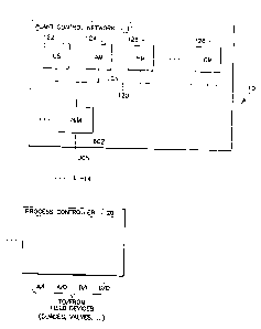
Figure 1 shows a block diagram of a process control
system in which the present invention can be utilized;
Figure 2 shows a block diagram of a process
controller, including I/O modules, in which the present
invention can be utilized;
Figure 3 shows a block diagram of an I/O module which
interfaces with the apparatus of the present invention;
Figure 4 shows a block diagram of the transmission
system of the present invention;
Figure 5 shows a timing diagram of the signals used
in the transmission system of Figure 4;
Figure 6 shows a logic diagram of the encoder of the
apparatus of the preferred embodiment of the present
invention:
Figure 7 shows a timing diagram of the generation of
a logic one signal by the encoder for transmission on a
fiber link;
Figure 8 shows a timing diagram of the transition
from the quiescent state to the start of data flow;
Figure 9 shows a logic diagram of the decoder of the
preferred embodiment of the present invention: and
Docket I2000064 4 2 July 1990
204~~3~
Figure 10 shows a timing diagram of the operation of
the decoder of Figure 9.
DETAILED DESCRIPTION
Before describing the apparatus and method of the
present invention, it will be helpful in understanding a
system environment in which the apparatus of the present
invention can be utilized. Referring to Figure 1, there
is shown a block diagram of a process control system 10 in
which the apparatus of the present invention can be found.
l0 The process control system 10 includes a plant control
network 11, in which a process controller 20 is
operatively connected to the plant control network 11 via
a universal control network (UCN) 14 to a network
interface module (NIM) 602. In the preferred embodiment
of the process control system 10, additional process
controllers 20 can be operatively connected to the plant
control network 11 via a corresponding UCN 14 and a
corresponding NIM 602. The process controller 20,
interfaces analog input and output signals, and digital
input and output signals (A/I, A/O, D/I, and D/O,
respectively) to the process control system 10 from the
variety of field devices (not shown) which include valves,
pressure switches, pressure gauges, thermocouples,....
The plant control network 11 provides the overall
Docket I2000064 5 2 July 1990
20~~~39
supervision of a controlled process, in conjunction with
the plant operator, and obtains all the information needed
to perform the supervisory function, and includes an
interface with the operator. The plant control network 11
includes a plurality of physical modules, which include a
universal operator station (US) 122, an application module
(AM) 124, a history module (HM) 126, a computer module
(CM) 128, and duplicates of these modules (and additional
types of modules, not shown) as necessary to perform the
required control/supervisory function of the process being
controlled. Each of these physical modules is connected
to a local control network (LCN) 120 which permits each of
these modules to communicate with each other as necessary.
The NIM 602 provides an interface between the LCN 120 and
the UCN 14. A more complete description of the plant
control network 11, and the physical modules can be had by
reference to U.S. Patent No. 4,607,256.
Referring to Figure 2 there is shown a block diagram
of the process controller 20, which includes the apparatus
of the present invention. The process controller 20 of
the preferred embodiment of the process control system 10
includes a controller A 30 and a controller B 40, which
effectively operate as a primary and secondary controller.
Controller A 30 and controller B 40 are connected to the
UCN 14, the UCN 14 in the preferred embodiment, comprising
Docket I2000064 6 2 July 1990
20~~~~~a
for communication redundancy purposes, a UCN(A) 14A and a
UCN(B) 14B. Input output (I/O) modules 21 interface to
field devices, field devices being various valves,
pressure switches, pressure gauges, thermocouples,.
which can be analog inputs (A/I), analog outputs (A/O),
digital inputs (D/I), and digital outputs (D/O). The
controller A 30 interfaces to each I/O module 21 via a bus
A 22, and controller B 40 interfaces to each I/O module 21
via a bus B 23. In addition, once again for communication
redundancy purposes, controller A 30 is also connected to
bus B 23 and controller B 40 is connected to bus A 22.
Controller A and controller B, 30, 40, can
communicate with each other via three mediums, the UCN 14,
a link 13 between the controllers, and the buses A, B, 22,
23, and bus A and bus B in the preferred embodiment being
serial I/O Links. One controller (controller A 30 or
controller B 40) operates as a primary controller and the
other controller operates as a secondary controller (in
more of a reserve mode than a back-up, in that if a
failure of controller A 30 should occur, controller B is
ready to take over the control function with essentially
no start-up or initialization time). On a predetermined
time basis, point processing is performed by the
controller designated as the primary controller and
communicates with the I/O modules 21. In addition, the
Docket I2000064 7 2 July 1990
NO~~~~
controller acting as the primary controller communicates
with the plant control network 11 reporting status,
history, and accepting inputs from the plant control
network such as commands from the operator via the
universal station 122. In addition, a data base
maintained by the primary controller is communicated to
the secondary controller via link 13. As mentioned above,
one controller operates as a secondary controller;
however, it will be understood by those skilled in the art
l0 that a secondary .controller is not necessary for the
process controller 20.
Referring to Figure 3 there is shown a block diagram
of an I/O module. A transceiver (anti-jabber circuit) 201
interfaces with bus A 22 and bus B 23. The transceiver
201 interfaces with a microcontroller (u-controller) 202
which, in the preferred embodiment, is of the type, Intel
80031. The microcontroller is coupled to a local bus 203,
and includes an EPROM 204 and a RAM 205 also attached to
the local bus 203. The RAM 205 contains the information
which forms the database for the I/O module 21. The EPROM
204 contains the program information utilized by the
microcontroller 202. Also attached to local bus 203 is an
input buffer 206 which receives the I/O link address
information from the I/O link (bus A, bus B, 22, 23). The
output buffer (BUFFER OUT) 208 is connected to the local
Docket I2000064 8 2 July 1990
204899
bus 203. The application specific circuits 209 is also
connected to the local bus 203 and interfaces with the
input and output buffers 206, 208, and the microcontroller
202 via the local bus 203. The application specific
circuits 209 vary from I/O module to I/O module depending
on the field device to which the I/O module is to be
coupled. If the field device is of a type which requires
a digital input, then the application specific circuit 209
will include the logic in order to place the digital input
into a predefined format which will interface with the
remainder of the I/O module. Likewise, if the field
device is such that requires an analog input, then the
application specific circuit contains logic which converts
the analog input signal (via an A/D converter) into a
format again consistent with predefined formats. In this
manner, the I/O modules are referred to as a specific I/O
module type. The microcontroller 202 performs the I/O
processing (or preprocessing) for the application specific
circuits 209. The preprocessing will vary from each I/O
module 21 depending on the type (i.e., A/I, A/0,...) the
preprocessing essentially consisting of translating the
signals from the application specific circuits to a format
compatible with the controller 30, 40, and putting the
signals from controller 30, 40 in a format compatible with
the I/O module 21. Some of the preprocessing performed
Docket I2000064 9 2 July 1990
2~~~~3~
includes zero drift, linearization (linearizing
thermocouples), hardware correction, compensation (gain
compensation and zero compensation), reference junction
compensation, calibration correction, conversions,
checking for alarms (limits)... and generating a signal in
a predetermined format having predetermined scale (i.e.,
engineering units, normalized units, percent of
scale,...). In the preferred embodiment seven types of
applications specific circuits are provided for, these
to include a high level analog input, low level analog input,
analog output, digital input, digital output, smart
transmitter interface, and pulse input counter.
In some configurations (see Figure 2), and in
particular when the distances between controller A 30 and
the IOP modules 21, become relatively large, the bus A 22
can be susceptible to noise, .... In order to reduce
these disturbances, a fiber optic link can be utilized.
Referring to Figure 4, there is shown a block diagram of a
serial digital data transmission system of the preferred
embodiment of the present invention which includes an
optical fiber link 51 (sometimes referred to herein as
fiber optic link or fiber link) between the controller 30
and the IOPs 21. (The redundant controller. 40 and the bus
B 23 are omitted here for simplicity.) An apparatus 60 of
the present invention provides an interface between the
Docket 12000064 LO 2 July 1990
2~ ~~93~
metallic link 22 (which is the backplane wiring for the
IOPs which also form part of the bus A 22 in the preferred
embodiment of the process control system 10) and the fiber
link 51. The controller 30 includes an I/O unit 31 which
also includes the logic of apparatus 60. The transmit
terminals (T) of apparatus 51 are connected to an electro-
optical converter (E/O) 52 and the receive terminals R of
I/O unit 31 are connected to an optical-electrical
converter (O/E) 53, the O/E 53 being connected to the
fiber link 51' from the E/O 52. The apparatus 60 of the
present invention includes a receiver/transmitter (R/T) 61
for coupling signals between the metallic link 22 and the
apparatus 60. Signals received from I/O unit 31 via o/E
52' are coupled from the R terminals of apparatus 60 to a
decoder 62, and the output signal of the decoder is
coupled to the metallic link 22 via R/T 61. Signals
received by the apparatus 60 from any of the IOPs 21 via
R/T 61, are coupled to an encoder 63 and the output of the
encoder is subsequently coupled to the T terminals of
apparatus 60 for transmission on the fiber link 51. The
apparatus 60 of the preferred embodiment of the present
invention will be discussed hereinunder.
In the operation of the system of Figure 4, the IoPs
21 are online and awaiting (listening) for communication
on the metallic link 22 from controller 30 (the controller
Docket I2000064 11 2 July 1990
20'~ ~~~9
30 includes a plurality of modules which are connected via
a metallic link 22', the I/O unit 31 also including logic
corresponding to the apparatus 60). In the quiescent
sta4e, there is no signal on the metallic link 22 (i.e.
the metallic link i5 inactive). Thus a signal A PLUS, A
MINUS, on the metallic link is shown in Figure 5, i.e. in
the preferred embodiment it is a balanced line. The fiber
link 51 is always active even in the quiescent state and
transmits a "1" data bit, FIBERSIG, as a string of DO
during the quiescent state. When the IOP 21 wishes to
communicate with controller 30, it begins by transmitting
a "0" followed by a valid character. Upon receiving valid
characters from the metallic link, the apparatus 60 turns
on a driver (not shown) to drive the fiber link 51' with
the valid character. At the receiving end, the decoder
(of the I/O 31 not shown) turns on an associated driver
(not shown) to drive the metallic link 22'. This
generally describes a transmission from IOP 21 to
controller 30. It will be understood by those skilled in
the art that a similar operation occurs for a
communication from controller 30 to IOP 21 via fiber link
51 " . The transition of the "1" on the fiber link to a
"0" (at the beginning of the transmission from the IOP of
the character received from the metallic link) bears no
phase relationship to what the fiber was transmitting in
Docket I2000064 12 2 July 1990
2~4~9~~
the quiescent state, since all the IOPs and the apparatus
60 each have their own clocking circuit. Figure 5 shows a
condition relating to the above discussion. The signal
(FIBERSIG) on the fiber link 51 transmits "1's" during the
quiescent state of the metallic link 22 (shown as bits
DO). At any point in time a digital data stream can be
initiated onto the metallic link 22, the first bit (D1)
being a "0". The figure depicts the bit D1 being started
before the end of the "1" data bit DO on the fiber link.
In this fashion the phase relationship can be immediately
established.
Referring to Figure 6, there is shown a logic diagram
of the encoder 63 of the apparatus 60 of the preferred
embodiment of the present invention. The balanced lines
of metallic link 22 couple the signals A PLUS, A MINUS to
the differential driver/receiver 61. In the preferred
embodiment of the present invention a circuit DS3695, well
known to those skilled in the art, is utilized. The
output of the driver/receiver 61 is a signal DAINO which
is coupled to the encoder 63. The input signal TMDATA is
a signal obtained from the controller 30 which is to be
coupled to the metallic link 22 for the IOPs 21. Although
only the apparatus 60 connected to the metallic link 22 of
the IOPs will be discussed, it will be understood by those
skilled in the art that the logic of the I/O unit 31 of
Docket I2000064 13 2 July 1990
2~~~9~~
the controller 30 operates in the same manner for
transmissions to apparatus 60 and receipt of data from
apparatus 60.
Still referring to Figure 6, the encoder 63 will nova
be discussed. The signal from driver/receiver 61, DAINO,
is inputted to a first flip flop (FF1) 601. In the
quiescent state, DAINO is high (for a logic one for a
positive logic). After four clock times the first flip
flop 601, and a second, third, and fourth flip flop (FF2,
FF3, and FF4) 602, 603, 604, respectively, connected in a
shift register arrangement will alI be high. A counter
610 will continue to count clock pulses when the input to
the clear terminal is low. The output of FF2 602 is
inverted by an invertor 611 and coupled to an AND-gate
612. The output of FF4 604 is also connected to AND-gate
612. The output of the AND-gate 612, connected to the
clear terminal of counter 610 will be low during the
quiescent state since the signal outputted from flip flop
2 is inverted from high to Iow thereby disabling AND-gate
612. The counter 610, a four bit binary counter, has the
second output QB connected to a first exclusive OR-gate
620, the third output QC coupled to the first exclusive
OR-gate 620 and to a second exclusive OR-gate 621, and a
fourth output QD connected to the second exclusive OR-gate
621. The output from the first exclusive OR-gate 620 is
Docket I2000064 14 2 July 1990
204~~~~
inverted by an invertor 622 and connected to a NAND-gate
623. The output of the second exclusive OR-gate 621 is
connected to the NAND-gate 623. The output of the NAND-
gate, D6, is then coupled to flip flop 6 (FF6) 606, the
output of flip flop 6 606 being coupled to an exclusive
OR-gate 625. The output of flip flop 2 602 is also
coupled to the exclusive OR-gate 625. The output of
exclusive OR-gate 625, XORS is connected to a fifth flip
flop (FF5) 605 and the output of FF5 605, denoted DAOUT is
coupled to a driver 628. The driver in the preferred
embodiment of the present invention is of the type DS8922D
well known to those skilled in the art. The output of the
driver 628 is the output of the encoder which is coupled
to the electro/optical converter 52. The outputs of
counter 610 are combined in the exclusive OR-gates and
NAND-gate 620, 621, 622, 623 to generate the output signal
D6 which is a four clock wide pulse essentially in the
center of the time period comprising sixteen clock pulses,
indicated in Figure 7. Figure 7 shows a timing diagram of
the apparatus 60 for generating the output quiescent data
pulse defined as a "1". The output of flip flop 5,
denoted DAOUT applied to the driver/receiver combination
of E/0 52, so that the signal appearing on the fiber link
51 is as depicted in Figure 5. It will be obvious to
those skilled in the art that the signal on the fiber link
Docket I2000064 15 2 July 1990
2~:'~9~~~
51 being transmitted is an optical signal and is depicted
in Figure 5 such that the "0" corresponds to the light
being on and the "1" condition where the light is off.
Referring to Figure 8, there is shown a timing
diagram of the transition from the quiescent state to the
start of data flow, i.e. being "1" to "0" transition which
is the start bit. In Figure 8 it is assumed for example
purposes only that the input data DAINO switches from the
high state to low state indicating the "0" bit for the
start of data. This occurs at some random clock time
selected here for example purposes to be during clock time
five. As a result the first through fourth flip flop 601-
604, all switch to a low state one clock time after the
previous flip flop switches, as shown. As a result of the
action of AND-gate 612, the counter stops counting when
the second flip flop switches low and starts counting
again when the second input from flip flop 4 switches to a
low state. The outputs of the counter are combined and
output the signal D6. The resultant output from combining
all the signals is shown in Figure 8 and the "0" bit is
specifically identified two clock times after the data has
switched. Note also that DAINO then switches to a "1",
for example purposes only and starts the waveforms for the
"1" state (after clock 16). This has already been
described for the quiescent state and is a simple exercise
Docket I2000064 16 2 July 1990
204~~ ~~
to continue the waveforms and derive combinations in
showing the output "1" bit from flip flop 5 to have the
waveform as shown in Figure 7.
Referring to Figure 9, there is shown a logic diagram
of the decoder 62 of the preferred embodiment of the
present invention. A receiver 671 accepts the input
signal FDRX from the O/E 52' and couples the inputted
serial digital data stream, or serial digital data signal,
through a flip flop 672 to a shift register 673 (the input
signal being denoted FDATIN). The receiver 671 is of the
type DS8922R well known to those skilled in the art. The
outputs of the shift register 673 are coupled to a first
NAND-gate 674 and to a second NAND-gate 675, with some of
the outputs being inverted. When a "0" bit is detected,
the first NAND-gate 674 outputs a ZERO signal and when an
"1" bit is detected, the second NAND-gate 675 outputs a
ONE signal. The outputs of the first and second NAND-
gates are as indicated in Table 1 below. The outputs from
the NAND-gates 674, 675 are then coupled through a series
of flip flops, and in particular the signals are latched
in JK flip flops 676, and 677, the output of JK flip flop
677 being coupled to the receiver/transmitter 61 to be
coupled onto the metallic link 22. Figure 10 shows a
timing diagram of the operation of the decoder of Figure
Docket I2000064 17 2 July 1990
2~4~939
TABLE 1
CLOCK INTERVAL
INPUT
DATA 1 2 3 4 5 6 I 8 9 10 11 12 13 14 15 16 OUTPUT
STREAM
ZERO DATA X X 1 1 1 1 1 1 0 0 X X X X X X ZERO = TRUE
I
ONE DATA ~ X X 0 0 0 0 0 0 1 X X X X X X ~ ONE = TRUE
1
WHERE X = DON'T CARE
Docket I2000064 18 2 July 1990
2~ ~~~~~
9. In a similar manner, the decoding of a "1" bit can be
shown.
While there has been shown what is considered a
preferred embodiment of the present invention, it will be
manifest that many changes and modifications can be made
therein without departing from the essential spirit and
scope of the invention. It is intended, therefore, in the
annexed claims, to cover all such changes and
modifications which fall within the true scope of the
invention.
Docket I2000064 19 2 July 1990