Note: Descriptions are shown in the official language in which they were submitted.
2 0 ~ 975
MOTION SIGNAL DETECTING CIRCUIT
Background of the Invention
The present invention relates to a system for smoothing
or spreading transitions between image regions included in
television signals to be tIansmitted which are processed in
a still picture signal processing method and a motion
picture signal processing method, and particularly to a
circuit for accurately detecting a motion signal which
represents a moving image, so as to control the transitions
between image regions of a frequency-unfolded image signal.
Standard television system such as an NTSC or a PAL
system, which represent images, processes a television
signal adaptively in accordance with an amount of motions of
the signal. This adaptive processing of the signal may
result in quasi-motion picture regions between image regions
being processed in a still picture signal processing method
and other image regions being processed in a motion picture
signal processing method. If differences in the processing
methods are perceived and, the different regions and the
transition between them are discerned by a viewer, image
quality is degraded.
For example, for the purpose of separating chrominance
and luminance components from a composite video signal, a
;~4~397S
frame comb filteI or a line comb filter may be used. As
long as there is no change in the image signal at frame time
intervals, when separating chrominance and luminance
components from the composite video signal using the frame
comb filter, the luminance and chrominance components can be
completely separated. If the scene changes, however, over
the frame time intervals, then some color information will
be present in the separated luminance component and some
brightness information will be present in the chrominance
component.
A line comb filter also used to separate the
luminance and chrominance components from the composite
video signal does not produce significantly degraded
component signals in the presence of image motion. However,
the line comb filter reduces the vertical resolution of the
reproduced image in comparison with the frame comb filter.
In addition, in locations where a vertical transition
occurs, an image processed by the line comb filter may be
degraded due to both color information introduced into the
luminance component, producing an image artifact known as
hanging dots and brightness information introduced into the
chrominance, producing incorrect colors in the neighborhood
of the transition.
Therefore the television signal is adaptively processed
by detecting the presence or absence of image motion. In
the regions in which the image is stationary, the frame comb
204~975
. .
filter is used, and in the regions in which the image is
moving, the line comb filter is used.
Another example of such adaptive processing is an
adaptive double-scanned, non-interlaced scan converter. In
such a converter, interstitial lines are displayed between
lines of the current field. However, the interstitial lines
may be those transferred from the preceding field, in the
presence of image changes producing visible artifacts such
as serrated contours. The interstitial lines may also be
interpolated from lines within the current field, but the
vertical resolution is reduced and line flicker may occur.
In regions in which image changes are detected, intrafield
interpolated interstitial lines are displayed and field-
delayed interstitial lines are displayed in other way.
Yet another example is an adaptive peaking circuitry in
which regions having relatively high noise are processed
with a relatively low peaking factor and regions having
relatively low noise are processed with a relatively high
peaking factor.
In all of the above examples, the television signals
are processed adaptively in response to the values of
estimated parameters of the image. The parameters are a
motion in the case of luminance/chrominance separation and
double scanning non-interlaced conversion, and a relative
level of noise in the case of the peaking. Differently
-
processed regions, and noticeable boundaries between regions
where the parameter is present and those where it is absent
are undesirable artifacts introduced by the above types of
adaptive processing types.
Co-pending Canadian Patent Application No. 2,056,744 on
an invention entitled ~'An improved video signal recording
system" filed on Dece~mber 2, 1991 by Samsung Electronics
Co., Ltd., describes a recording system for recording and
reproducing a full bandwidth video signal on and from a
recording medium having a limited bandwidth by folding the
high frequency component of a luminance signal into the low
frequency component of the l-lm;n~nce signal.
In co-pending Canadian Patent Application No.
2,056,744, a motion signal which represents a moving image
is recorded together with the folded ll1min~nce signal and
the chrominance signal on the recording medium. The motion
signal is used to control the transition between regions of
the full bandwidth ll1m;n~nce signal which is unfolded into
the original frequency bands when reproducing.
That is, in the above prior art, the high frequency
component of the luminance signal is folded into the low
frequency component of the lum;n~nce signal in recording.
At this time, the high frequency component of the luminance
signal is modulated by a folding carrier, so that the folded
lnm;n~nce signal has a phase difference of 180 degrees
between frames, between scanning lines, and between pixels.
2~ 4~ 9~ S
Accordingly, in reproducing, the high frequency component
folded into the low frequency component of the folded
luminance signal is demodulated by the unfolding carrier
having the same phase and frequency as those of the folding
carrier, so that the hish frequency component of the
luminance signal is unfolded to the originai frequency band.
However, the folding carrler and the sideband thereof
will be present in the unfolded luminance signal. The
resultant luminance signal unfolded by the folding carrier
and the sidebands thereof has a phase difference of 180
degrees between frames.
As a result, the conventional motion signal detecting
circuit for detecting the level difference of pixels between
fames as the motion signal, has difficulty in detecting
accurately the motion signal from the unfolded luminance
signal due to the phase off-set between frames.
Summary of the Invention
It is an object of the present invention to provide a
motion signal detecting circuit for accurately detecting a
motion signal which represents a moving image from the
unfolded luminance signal.
To achieve the above object, a motion signal detecting
circuit according to the present invention comprises: an
20~8975
input line for receiving an unfolded luminance signal;
means for eliminating a folding carrier and sidebands
thereof contained in the unfolded luminance signal; and comb
filter means for detecting a motion signal which is a
difference component between frames of the unfolded
luminance signal from the output of the eliminating means.
Brief Description of the Drawings
The object and features of the present invention will
become more readily apparent by the following detailed
description of the preferred embodiment in conjunction with
the accompanying drawings in which:
FIG. 1 is a block diagram of a circuit to control
transitions between image regions included in the unfolded
luminance signal to be transmitted in a video reproducing
apparatus to which the present invention is adaptedi
FIG. 2 is a block diagram of a preferred embodiment of
a motion signal detecting circuit according to the present
invention;
FIG. 3 is a detailed circuit diagram of the prefilter
adapted in the motion signal detecting circuitry in FIG. 2;
and
FIG. 4 is a detailed circuit diagram of the signal
spreader adapted in the motion signal detecting circuitry in
FIG. 2.
2 ~ 7
Detailed Description of the Invention
In FIG. 1, an input line 5 is connected to a frequency
unfolding circuit which is not shown for receiving an
unfolded luminance signal. The input line 5 is connected
to respective input terminals of a temporal low pass filter
10, an adaptive spatial low pass filter 20 and a motion
signal detecting circuit 40. An output terminal of the
temporal low pass filter 10 is connected to a first input
terminal of a soft switch 30. An output terminal of the
adaptive spatial low pass filter 20 is connected to a second
input terminal of the soft switch 30. An output terminal of
the motion signal detecting circuit 40 is connected to a
control terminal of the soft switch 30. An output terminal
of the soft switch 30 is coupled with an adaptive peaking
circuit which is not shown through an output line 15.
In operation of the circuit as shown in FIG.1, when the
level of motion is low, the unfolded luminance signal Luf
inputted through the input line 5 lies at temporal low
frequencies (close to temporal direct current component).
On the contrary, the level of motion is high, the unfolded
luminance signal Luf inputted through the input line 5 lies
at spatial low frequencies. Accordingly, in the presence of
a high level of motion, the image may overlap temporally
with the unfolded luminance signal. In the presence of a low
2~ 375
level of motion, the image may overlap spatially with the
unfolded luminance signal Luf.
The temporal low pass filter 10 separates a temporally
derived luminance signal Lt from the unfolded luminance
signal Luf by temporally filtering the unfolded luminance
signal Luf.
The adaptive spatial low pass filter 2G separates a
spatially derived luminance signal Ls from the unfolded
luminance signal Luf by adaptively and spatially filtering
the unfolded luminance signal Luf.
The motion signal detecting circuit 40 generates the
motion control signal M* by detecting the motion level of
the image from the unfolded luminance signal Luf.
The soft switch 30 controls the proportion of the
unfolded luminance signals Lt and Ls which are respectively
separated temporally and spatially from the unfolded
luminance signal Luf, in accordance with the motion control
signal M~ fed from the motion signal detecting circuit 40.
When a level of the motion control signal M* is zero or
nearly zero, the output of the soft switch 30 is the same as
that of the temporal low pass filter 10.
As the level of the motion control signal M* gradually
increases, the proportion of the input from the temporal
low pass filter 10 decreases and the proportion of the
input from the adaptive spatial low pass filter 20
increases. When the level of the motion control signal M*
~ 7gS
is relatively high, the output of the soft switch 30 is the
same as that of the adaptive spatial low pass filter 20.
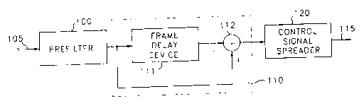
FIG. 2 shows a block diagram of a motion signal
detecting circuit according to the present invention.
In FIG. 2, an input line 105 is connected to the input
line 5 shown in FIG. 1 and an input terminal of a prefilter
100, respectively.
An output terminal of the prefilter 100 is connected to
an input terminal of a frame delay device 111 and a second
input terminal of a subtracter 112. An output terminal of
the frame delay device 111 is coupled with a first input
terminal of the subtracter 112. An output terminal of the
subtracter 112 is connected to an input terminal of a
control signal spreader 120. An output terminal of the
control signal spreader 120 is connected to a control
terminal of the soft switch 30 shown in FIG. 1 through an
output line 115.
In operation of the circuit as shown in FIG.2, the
prefilter 100 eliminates the folding carrier' and sideband
contained in an unfolded luminance signal Luf by filtering
the unfolded luminance signal Luf received thIough input
line 105. The construction of the prefilter 100 is
described in the U.S. patent application No. 07/562,907 on
the invention entitled "An improved apparatus for
eliminating the folding carrier and sidebands from the
21 1~8~7S
,. .
unfolded luminance signal" filed on August 6, 1990, by Ko.
et al., which may be desirably comprised of the circuit as
shown in FIG. 3.
Referring to FIG. 3, equal amplitudes of the unfolded
luminance signal on input line 310 are passed through the
horizontal comb filter 311 and the vertical com~ filter 312,
and, unless affected by multipliers 314 and 319, equal
amplitudes of the two signals are combined in adder 316 and
the sum is available at the output 317. The horizontal
comb filter 311 is designed to cancel the sidebands of the
folding carrier at or above 2.5MHz, and the vertical comb
filter 312 is designed to cancel the line frequency of
15,734Hz. However, the cancellations of the carrier and
sidebands may be incomplete since they are affected by the
brightness variations in the picture being scanned.
Cancellations of the horizontal and vertical carriers on the
output line 317 is achieved by the operation of the vertical
scan edge detector 321 and the horizontal scan edge detector
322. When a "vertical'l edge or discontinuity is detected
during a vertical scan, a signal over line 323 and through
subtracter 324 to the look-up table 327 causes a signal
having a value of K over line 328 from look-up table 327 to
increase the proportion of the output at 317 from the
horizontal comb filter 311, whose output is not affected by
the vertical edge, and decrease the proportion from the
vertical comb filter 312. Likewise, when a "horizontal~
~ 7 ~
edge is detected during a horizontal scan, a signal over
line 325 and through subtracter 324 causes a signal having a
value of K over line 328 both to increase the proportion of
the output at 317 from the vertical comb filter 312 whose
output is not affected by the horizontal edge, and decrease
the proportion from the horizontal comb filter 311. In
each cas~e, the cancellation of carrier components is
improved by increasing the output proportion from the comb
filter whose output is not affected by the brightness edge
encountered.
In FIG. 2, the frame delay device 111 delays by a time
corresponding to one frame the unfolded luminance signal
from which the folding carrier and sidebands are eliminated,
and suppIies it to the first input terminal of the
subtracter 112.
The subtracter 112 subtracts the output of the frame
delay device 111 from the output of the prefilter 100,
generates the difference signal between frames of the
unfolded luminance signal, and supplies it to the control
signal spreader 120 as the motion signal.
The frame delay device 111 and the subtracter 112
constitute a comb-filter.
The control signal spreader 120 spreads the motion
signal temporally, vertically, and horizontally, and
supplies the spread signal to the control terminal of the
~- soft switch 30 shown in FIG. 1 as the motion control signal.
The control signal spreader 120 can be constructed in
the same manner as "The control signal spreader" described
in co-pending Canadian Patent Application No. 2,036,175 on
an invention entitled "A control signal spreader", filed on
February 12, 1991, by Ko. et al., which may be desirably
comprised of the circuit as shown in FIG. 4.
Referring to FIG. 4, the horizontal widener 402 has an
input terminal 414 connected to a series of six clock delays
416 through 426. The output of an OR gate 428 is connected
to an output terminal 430, and seven inputs of the OR gate
428 are respectively connected to the input terminal 414 and
the ends of the clock delays 416-426 that are remote from
the input terminal 414. Any motion signal having an
similitude of 1 indicating the presence of a phenomenon such
as motion will be repeated six times at the output terminal
430.
The vertical widener 404 comprises four 1-H delays 432,
434, 436, and 438 connected in series to an input terminal
431 and OR gate 440 of which the output is connected to an
output terminal 442 and five inputs are respectively
connected to the input terminal 431 and the ends of the 1-H
delays 432-438 that are remote from the input terminal 431.
Any line of motion signals applied to the input terminal 431
will be repeated four times at the output terminal 442.
The motion signals having the logic value of 0 pass
12
A
2~ B~375
through hoIizontal widener circuits 402 and vertical widener
circuit 404 without and delay and the logic value of 1,
indicating the presence of a ph~enomenon such as motion, is
repeated so as to form a rectangle of logic l's that is 7
clock cycles wide and 5 lines high.
The line signal spreader 406 is coupled to the output
terminal 444 of the vertical widener 404 and functions to
produce a ramp of increasing signal values along a line that
increases from the value of 0 to a maximum value, such as 7,
durin-g the first 6 motion signal periods referred to. It
then holds the maximum value as long as l's appear at the
terminal 444, and when they cease, it produces a ramp of
decreasing signal values along the line over a period of 6
clock cycles. This is done in the same way along the line
whenever the motion signal assumes the logic value of 1, and
along the 4 succeeding lines so that there are 5 identical
lines.
For performing the line signal spreading function ~ust
described, a MUX 446 has an output 448, an input labeled O,
an input labeled 1 and a switching control input 450 to
which logical values of 0 and 1 may be applied. When a
logic 0 is applied to the control input 450, the output 448
is connected to the input labeled 0, and when a logic 1 is
applied to the input 450, the output 448 is connected to the
input labeled 1. A one clock delay element 452 and a
2 ~ 7~
generator 454 that performs the function f(x)=x-1 are
connected in series between the output 448 and the input
labeled 0. The generator 454 cannot go below a value of 0.
Thus, whe~n ns motio-n is detected and a logic o is at the
input terminal 400, logic O~s are passed through the widener
circuits 402 and 404 tG the terminal 444, and the output 448
of the MUX 446 will be 0. If by some c*ance the signal at
the output 448 of the MUX 446 should be other than 0. It
will be reduced to 0 in at most 4 clock cycles by the
opeIation of the generator 454. As will be seen, the MUX
446 will produce the ramp of decreasing values previously
referred to.
The ramp of increasing value:s, previously referred, to
is formed by a MUX 456. It has an output 458 that is
connected to the input of MUX 446 that is labeled 1, an
input labeled o, an input labeled 1 and a switching control
input 460 to which logic values of 0 or 1 may be applied.
As in the MUX 446, a logic 1 at the control input 460
connects the output 458 to the input labeled 1, and a logic
0 at the control 460 connects the output 458j to the input
labeled 0. A one clock delay 462 and a generator 464 that
performs the function f(x)=x+1 are connected in series
between the output 458 and the input labeled 1. The
generator 464 cannot produce a signal value above some
selected maximum, such as 7. The input of the MUX 456 that
is labeled 0 is coupled to the output 448 of the MUX 446.
14
2~3~7~
. .,
For making the signal values for corresponding pixels
along the scan lines available, the vertical signal spreader
408 comprise four l-H delays 466, 468, 470 and 472 and an
adder 474 for adding the output 448 and the outputs of the
four l-H delays 466 though 472.
Here, the motion signal values at the output 448 and at
the ends of the four l-H delays 466 through 472 that are
remote from the output 448 c~ould be respectively weighte-d
before they are combined in the means for combining them,
that is, an adder 474. Also, the temporal spreader 410 is
suitably composed of a low-pass filter. It provides gradual
transitions between still and motion portions of a scene in
the temporal domain. The output of the temporal spreader 410
is supplied to the control switch 30 of FIG.l through an
output line 115. Here, the output line 412 is identical with
the output lin~e 115 of FIG.2.
As described above, according to the present invention,
it is possible to detect the motion signal from the unfolded
luminance signal by utilizing a comb filter after removing
the folding carrier and the sidebands thereof contained in
the unfolded luminance signal by the prefilter.
In addition, by spreading the detected motion signal
temporally, vertically and horizontally by the control
signal spreader and supplying the spread motion signal as
the motion control signal, undesirable artifacts due to the
2~!37~
,. ~
distinct boundaries between image regions can be removed.
16