Note: Descriptions are shown in the official language in which they were submitted.
WO90/11650 2 0 4 8 9 9 ~ PCT/US90/01362
DIGITAL CIRCUIT FOR ENCODING
BINARY INFORMATION
05 CROSS-REFERENCE TO RELATED APPLICATIONS
This application is related to Application
Serial No. 206,407 filed June 19, 1988, by Wash; to
Application Ser. No. 206,408 filed June 14, 1988 by
Whitfield et al.; to Application Ser. No. 206,553
10 filed June 14, 1988, by Whitfield; to Appli~ation
SerO No. Z06,646 filed June 19, 1988 by Wa~h; to
Application Ser. No. 07/327,073 filed on March 22,
1989, by C. Chi, which is being filed
contemporaneously with this application; and to
15 Application Ser. No. 07/327,068 filed on March 22,
1989 by F. Silva, which is being filed
contemporaneously with this application. The entire
disclosures of each of these applications are
incorporated by reference herein. Each of these
20 applications is copending and commonly assigned.
FIELD OF THE INVENTION
This invention relates to electrical
circuits suitable for encoding binary information,
in accordance with a novel modulation method.
INTRODUCTION TO ~ INVENTION
A novel method for modulating binary data
or information into a format suitable for encoding
and decoding e.g., magnetic information or optical
information, is disclosed in the above-cited - -
30 Application Ser. No. 07/327,073-to C. Chi. The
novel method features self-clocking, velocity ---
insensitive encoding and decoding; The Chi
disclosure states that preferred electrical circuits
that may be employed for realizing the encoding
35 scheme set forth in that disclosure are provided in
WO90/11650 ~ ~4~ ~ 9 a PCT/US90/01362 ;~
the present application. This application,
therefore, provides novel electrical circuits that
may be advantageously employed, for e~ample, for
encoding bin~ry data or information into a format in
accordance with the Chi disclosure. The novel
electrical circuits encode the data, and preserve
the sel-clocking, velocity insensitive features of
the novel method.
SUMMARY OF THE INVENTION
The novel method of Chi is first set forth,
in order to provide a perspective for the present
invention.
Accordingly, Chi discloses a method for
modulating binary data comprising first and second
15 information, the ~ethod comprising:
(l) defining an event-cell as the time
between two adjacent clock transitions, the clock
transitions having a unique characteristic; and
(2) selectively writing the information
20 into,the event-cell at an arbitrary time, by
(i) generating a first event and a
corresponding first read signal, in response to the
first information; or
(ii) generating a second event and a
25 corresponding-second read signal, in response to the
second information.
. .With the intent of providing a means for
realizing the Chi method, I now disclose an
electrical.circuit suitable for encoding binary data
30 comprising first and second information, the ~-
electrical circuit.comprising~
- (l) a clock driver;
- (2) an n-phase counter driven by the clock
driver, the counter comprising
35 - a) means for producing a succession of
- Woso/1~650 2 ~ ~ 8 9 9 ~ PCT/US9~/01362
event-cells;
b) means for demarcating, in a first
event-cell, an arbitrary location of a first event,
in response to a first information; and
c) means for demarcating, in a second
event-cell, an arbitrary location of a second event,
in response to a second information;
(3) first means for generating a first
event in the first location, in response to a first
information; and
(4) second means for generating a second
event in the second location, in response to a
second informat~on.
8RIEF DESCRIPTION OF THE DRAWINGS
The invention is illustrated in the
accompanying drawing, in which:
Fig. 1 is a circuit diagram of the present
invention; and
Figs. 2A, B show waveforms processed by the
20 Fig. 1 circuit.
DETAILED DESCRIPTION OF THE INVENTION
I now disclose preferred aspects of the
present invention summarized above.
e clock driver preferably outputs a pulse
25 train havi-ng an arbitrary, but constant frequency.
A selected frequency helps determine the duratio~ or
length of an event-cell, and this duration, in turn,
may depend on the ultimate employment of the
circuit,~for example, as an optical or magnetic
30 encoder. A conventional clock driver may be
~ ", , -
employed for these purposes.
~ ~ ~ The n-phase counter, driven by the clock
- , . . ~:
driver, comprises means for producing a succession
of event-cells, and demarcates a succession of
35 event-cells by a set of unique clock transitions.
WO90/11650 2 ~ ~ 8 9 9 ~ PCT/US90/01362
For example, unique clock transi~ions can be defined
as those having an invariant negative polarity.
Associated with this point, the first and second
means for generating the first and second events,
respectively, leave invariant the set of unique
clock transitions. A conventional n-phase counter
may be employed for these purposes.
Preferably, an event-cell for a first
information is defined by a duration t, and has n
sub-units, each of duration ~ z t~n; and the means
for demarcating the first location in the first
event-cell comprises serial first, second and third
clock signals located at n -l, n, n +l, respectively.
2 2 2
Preferably, an event-cell for a second
information is defined by a duration t, and has n
sub-units, each of duration y ~ t/n; and the means
for demarcating the second location in the second
event-cell comprises a single clock signal located
at t/2.
Preferably, the first means for generating
the first event comprises a logic circuit that
functions so that, if its inputs are the first
information and the first or second or third clock
25 signals, then its output generates alternate `~
information transitions-at the locations --
n -1, n, n +1, respectively.
2 2 2
.. . . .
Preferably, the second means for generating
the second event comprises a logic circuit that
., ... . . ~ .. .
functions so that, if its inputs are the second
- . I .. . . _ .
information and the single clock signal, then its
output generates an information transition at the
location n/2.
Note that the first and second means
35 provide a two-fold function, viz., they operate to
20~8995
WO90/116~0 PCT/US90/01362
provide discrimination of the first and second
informations, and they leave invariant the unique
clock transition characteristic.
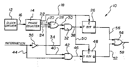
Attention is now directed to Fig. 1, which
shows a circuit 10 of the present invention. The
structure of the circuit 10 is first disclosed,
followed by its operation.
Accordingly, the circuit 10 comprises a
clock driver 12, and an n-phase counter 14 (n~10)
connected and driven by the clock driver 12, along a
line 16. The n-phase counter 14 can provide four
clock signal outputs, labeled Clock (CL),
n -1, n, n ~1, along lines 18, 20, 22, 24, and can
2 2 2
reset or recycle at the count 10. Further, the
clock signal (~L) output is an input, along the line
18, to a toggle flip-flop 26; and the other signal
outputs, namely n -1, n, n ~1, are inputs along the
2 2 2
lines 20, 22, 24 respectively, to an OR gate 28.
An output of the OR gate 28 becomes a first
input, along a line 30, to an AND gate 32. A second
input to the AND gate 32, along a line 34, carries
the inverted first and second informations, i.e.,
digital l's and 0's, as inverted by an inverter 36.
The-output-of the AND gate 32 is a second input to
the toggle flip-flop 26, along a line 38.
~ The circuit 10 is completed by observing
that the clock signal output n/2 is^a first input,
along a line 40, to a (second) AND gate 42. A
second:input to the-AND gate 42, along a line 94,
carries the first-and second informations, i.e.,
digital l's and 0's. The output of the AND gate 42,
along a line 46, becomes an input to a latching or
delay flip-flop 48. The latching flip-flop 48
receives, as well, the clock signal (CL) along a
WO90/11650 2 0 4 8 ~ 9 a PCT/US90/01362 '
line 50, and outputs a signal, along a line 52, to
an OR gate 54. The OR gate 54 also receives an
input signal along a line 56, from the-toggle
flip-flop 26. The output of the OR gate 54, on a
5 line 58, completes the structure of the circuit 10.
The operation of the Fig. 1 circuit 10 will
now be disclosed, and reference additionally will be
made to the waveforms shown in Figs. 2A, B. An
objective of the operation of the circuit 10 is to
10 encode a first binary information "0", in a first
event-cell, and then a second binary information
~'1", in a second event-cell.
To this end, a leading edge of the first
event-cell is produced by the combined operation of
15 the clock driver 12, the 10-phase counter 14, and
the flip-flops 26, 48. That is, in response to the
pulse train outputted by the clock driver 12 along -.
the line 16, the 10-phase counter 14 outputs a first
negative clock transition, Cl, by way of preset
20 lines (not shown), along the lines 18 and 50, to the
clear operations of the toggle flip-flop 26 and
latching flip-flop 48, respectively ~See Fig. 2B).
The flip-flops 26, 48, in turn, output (in this
illustrative embodiment)..a logic 0. This logic 0
25 output is provided, regardless of the:.state the
flip-flops 26, 48 may previously have been in, i.e.,
a logic 0 or logic 1. Accordingly, the logic 0
outputted by the flip-flops 26, 48, in turn, become
logic O inputs to the OR gate 54. The OR operation
30 results in.a logic 0 on-the circuit.10 output line
,. . . .
58, and corresponds to the Fig.-2A leading edge
. ~ .
(C1) of the first event-cell. : . -- '
~ As stated, it is desired to encode the
first information 0 in the first event-cell. This
35 may be accomplished by a first means for generating
.. .. ..... ". .~ ~ . ~.,,,j .
,
204899~
WO90/11650 PCT/US9OtO1362
a first event. The first means comprises the logic
elements 28, 32, 26, 54, which elements function so
that, if its inputs are the first information O and
the clock signals n -l or n or B +l, then its output
2 2 2
5 generates alternate information transitions (the
first event) at the first event-cell locations
n -1, n, n ~1, respectively, as shown in Fig. 2A.
2 2 2
Note that for this illustrative embodiment, n - lO,
so that the first event-cell locations are
lO identified as 4, 5, 6, in Fig. 2A.
The last paragraph is e~panded upon as
follows. The logic element 28, the OR gate, outputs
a logic 1 in response to three successive clock
signals, namely n -1, n, n +1 (Fig. 2B). The logic 1
2 2 2
15 becomes the line 30 input to the AND gate 32. The
AND gate 32 outputs a logic 1, along the line 38,
for each of the three successive clock signals,
since its two inputs, line 30 and line 34, each are
logic 1. (To this end, note the operation of the
2n inverter 36 on the information 0, to generate a
logic 1 on the line 34). Continuing, the line 38
logic 1 input to the toggle flip-flop 26, has the
effect of successively toggling the flip-flop 26,
for each of the successive clock si~nals
25 n -1, n, n ~1. The toggling action, as carried over
2 2 2
by the OR gate 54, produces three successive
information transitions at the first event-cell
locations 4; 5, 6, corresponding to the clock
30 signals n -1, ~, n +1, respectively.
2- -~-2- 2 ; -
-- The trailing edge of the first event-cell,
at location C2, is now generated in a manner
analogous to that of the leading edge Cl, above.
Wo90/l~650 2 ~ 4 8 9 9 ~ PCT/US90/01362
--8--
That is, the clock 12 and 10-phase counter 14, in
combination with the input on lines 18, 50 to the
flip-flops 26, 48 clear operation, results (by way
of the OR gate 54) in the circuit 10 output line 58
5 making a transition to logic 0, as shown in Fig. 2A.
The first information 0 has now been
encoded; the 10-phase counter 14 is reset (Fig. 2a),
and the circuit 10 can now encode the information 1
in a second event-cell. This may be accomplished by
a second means for generating a second event. The
second means comprises the logic elements 42, 48,
54, which elements function so that, if its inputs
are the second information and the single clock
transition n/2, then its output generates an
information transition at the location n/2, as shown
in Fig. 2A.
The last paragraph is expanded upon as
follows. The logic element 42, the AND gate,
outputs a logic 1 only when its inputs on lines 44,
40 are logic 1. This last case only occurs at the
time of the single clock transition n/2 (see Fig.
2B). Continuing, the AND gate 42 output, on the
line 96, in turn, becomes an input to the latching
flip-flop 48. The flip-flop 48 provides'an output
information transition (logic 1) in-'response to this
input, and outputs the information'transition to the
circuit 10 output line 58, by way of the OR gate
54. The flip-flop 48 holds the logic 1 until the
advent of'a subsequént line 50 clock signal input.
This last clock signal clears the flip-flop 48, as
well as the fIip-flop~26'(by way of line 18), thus
generating a trail'ing~èdge of the'second event-ceii
(C3), shown in Fig. 2A. The timing signals for ~'
this last operatiGn are shown in Fig. 2B.
3~ The operation of the circuit 10 has now
.: .
.
WO90/11650 2 0 ~ 8 9 9 ~ pCT/Us9o/ol362
been disclosed, and the following observations are
made. First, it is noted that the AND gates 32, 42
function to isolate the first and second event
generating means. Thus, inspection of Fig. 1 shows
that the AND gate 32 provides an isolation
capability for the second event generating means,
while conversely, the AND Gate 42 provides an
isolation capability for the first event generating
means.
Further, it is noted that the first and
second event generating means provide at least a
three-fold function: viz., (1) they may be located
at any arbitrary location within an event-cell;
(2) they leave invariant the (unique) negative
clock transition defining the advent of the
succession of event-cells; and (3) they operate to
provide encoded discrimination of the first and
second informations. On the last point: the first
and second events, namely the alternating sequential
first information transitions, versus the single
second information transitions, are such that in a
(downstream) decoding or reading operation, the
encoded information can be readily recovered.
Finally, in alternative embodiments (not
shown), it is possible to locate the alternating
seguential first informations at other arbitrary
locations, for e~ample, at clock locations 6, 7, ~;
and to locate the single information transition at
another arbitrary location, say, location 3.
Howevér, thé Fig. 2 locations are preferred because
they help minimize probiems of noise or
discrimination ambiguities. Related to this is the
point that, in alternative embodiments, it is
possible to generate first events comprising an
ar~itrary large odd number of alternating sequential
W090/11650 2 0 ~ 8 ~ 9 ~ PCT/US90/01362
--10--
first information transitions, and to generate more
comple~ second events. But in all alternative
embodiments, the generated first and second events
will be such that they leave invariant the clock
transition polarity, and ensure first and second
information discrimination.
The Chi method can also be encoded by a
software program running in a microprocessor,
computer, or microcomputer, and in accordance with
the claimed invention summarized a~ove. The
benefits of using this software approach depend on a
specific application. A suitable software encoding
routine written in ~ASIC computer language is listed
below. While this routine is not the only software
approach to encoding the Chi method, it is
representative of what can be done in many cases.
REM *~ CONSTANT CLOCK ENCODING ROUTINE ~
K~l0 SUBDIVISIONS OF EVENT CELL
DIM ARRAYl(DATAQTY~K) ARRAY FOR OUTPUT STREAM
DIM DATA(DATAQTY) ARRAY FOR INPUT BINARY DATA
I=0 SET OUTPUT ARRAY POINTER
FOR J-l TO DATA156 LOOP THROUGH BINARY DATA
FOR N-0 TO K-l LOOP THROUGH SUBDIVISIONS
IF N'3~AND DATA(J)~0 THEN ARRAYl(I)~l
IF N~4 AND DATA(J)'0 THEN ARRAYl(I)-0
100 IF N~4 AND DATA(J),l THEN ARRAYl(I).l
110 IF N~5 AND DATA(J)~0 THEN ARRAYl(I)~l
120 IF N<>3 OR 4 OR 5 THEN ARRAYl(I)~0 -- -.
30 130 I-I+l ~ INCREMENT OUTPUT ARRAY PTR
140 NEXT N STEP TO NEXT SUBDIVISION
150 NEXT J GET NEXT BINARY DATA BIT -
. .
- -
' - .' '
: -