Note: Descriptions are shown in the official language in which they were submitted.
2049433
ELON~-ATF SUPER~vNw~:~O~ ~r~MFNTS C~'MP~T~ING
OxTnP~ SupFR~ ND~cTQRs . SlIpERt~NDlJt'TTNG
COTT..~ AND M~rl'HODS OF MAT~TN~ SUCH ~T~T'M~NTS
This invention relates to elongate superconductor
elements comprising oxide superconductor materials, to
superconducting coils comprising such elements, and to methods
of making such elements. Oxide superconductor material herein
means material which is super~-~n~lr~jve in bulk, i.e. in which
the crystal grains are joined, e.g. by sintering or other
processes, to permit passage of superconducting current.
Since the discovery of oxide superconductors, efforts
have continued to be made in many fields to develop technology
for their use in industrial applications. Because oxide
superconductors have higher critical temperatures and cri~ical
magnetic field intensities than conventional metallic alloy
superconductors, their application to heavy electric fields,
once realized, will unlock an unpredictably wide range of
possibilities .
2 O To employ oxide superconductors in the heavy
2 2049433
electric field requires transforming them into suitable
wire products and forming these products into colls or
other forms of conductors. For ~u~el~:ul,ducting oxide
products to be used as coils, it is an essential
5 re~uirement that the conductor is able to pass a
sufficient amount of superconducting current in a
magnetic field to generate magnetic flux. When forming
superconductive oxides into conductive products which
have large critical current densities in a magnetic
10 field, it has been con~ red effective to orient the
c-axes of the crystals of the ~u~ ullductor material
in certain directions. There is therefore a need for
superconducting oxide wire products with oriented
crystals which are suited for drawing and coiling
15 operations and also to provide a method of
manufacturing such oxide superconductor products.
It has been found that wire products that are
suited for such purposes can be produced by using
yttrium oxide based superconductor materials and
20 forming metal-clad superconductors into wires of flat
cross-section, as mentioned in the Japanese Journal of
Applied Physics 27 (1988), pages 1715-1717, and in JP-
A-1 -251515
A~ter the discovery of bismuth and thallium oxide
25 materials, c- L L~ L:, were made to make wires using these
oxide materials. One example of fabrication of bismuth
3 2049433
( Bi ) oxide wire is aescribed in Low-Temperature
Engineering, 25 (1990), No. 2, pages 88-g3, and another
example of a thallium ( Tl ) oxide wire is discussed in
the Japanese Journal of Applied Physics, 27 (1988),
pages 2345-234~.
The superconductivity of an oxide superconductor
in a magnetic field, as pointed out in Physica C, 159
( 1989 ), pages 433-438, is known to he closely related
to the crystal orlentation relative to the direction of
magnetic field. If the crystal c-axes are oriented
perpendicularly to an external magnetic field, there is
little performance deterioration even when the
superconductors are sub~ ected to relatively high
magnetic iield. On the other hand, when the crystal c-
axes are parallel to the external magnetic field, the
superconductivity is lost to a large extent even . in a
small external field. JP-A-1-2g6801 (corresponding to
EP-A-2g2436 ) discusses this problem and proposes
orienting wire products differently at different parts
of a superconducting coil.
The e:~pert in this field will know the definition
of the c-axis and a-b plane of oxide superconductor
crystals, but reference may be made to Hitachi Review,
39 ( 1990 ), No. 1, pages 55-62 "Development of high-Tc
superconducting wire with high critical current
density " .
.
4 2049433
In the above-mentioned prior art, with the
exception of JP-A-1-246801 mentioned above, there is a
problem that conS~ fl~ration is not given to the
relationship between the direction of magnetic lines of
5 force and the direction of the conductor. In other
words, when sub~ected to a magnetic field parallel to,
rather than perpF~nfl i o~ r to, the crystal c-axes or to
a magnetic f ield extending in a direction that is
detrimental to the superconductivity, the wires with
10 the oriented c-axes sharply deteriorate in performance
as current conductors . r~nc~ flt:.r an example, in which
the previously proposed wire product is wound into a
solenoid coil and a current is applied to generate a
magnetic field. In this case, if the wire is coiled so
15 that the c-axes are perp~nfl~ r to the coil axis, the
wire close to the coil centre will exhibit the best
performance for that particular magnetic field
direction. At the end of the coil, however, since the
magnetic lines of force curve in, the angles between
20 the magnetic lines of ~orce and the c-axes are not
n~ qs~rily optimized and the coil may, depending on
the location, be used with magnetic lines of force
running parallel with the c-axes. Such a magnetic flux
distribution changes according to the magnetic field
25 intensity generated by the coil, so that this problem
cannot be solved by simply changing the coiling angle
2~49 433
at the end of the coil. The maximum current that can be
passed through the entire coil is limited by the portion of
the wire where the critical current is the lowest. That is,
5 if there is even a single part of the wire where the magnetic
flux is parallel to the c-axes or passes through the wire in
a direction detrimental to the superconductivity, the magnetic
field generated by the entire coil is limited.
The object of this invention is to provide an oxide
10 superconductor element whose critical current density will
not greatly fall when subjected to a magnetic field in any
particular direction and which is suitable for making a coil,
and to provide methods of making such elements.
According to the present invention in one aspect, there
15 is provided an elongate superconductor element having, as seen
in section perpendicular to its longitudinal axis, a plurality
of oxide superconductor material regions in each of which the
c-axes of most of the oxide superconductor crystals are
transverse to the longitudinal axis of the element and the
20 c-axes of the oxide superconductor crystals are generally
aligned with each other. The alignment directions of the
c-axes are different as between different ones of the
regions so that the element has a plurality of such
6 2049433
regions having respectively dif ferent c-axis ~ nm~nt
directions .
The ~ L~ ,t in this description and claims that
"the c-axes of most of the oxide ~u~L~Jlld~ctor
5 crystals are transverse to the longitudinal axis of the
element" means that more than 50% of the crystals have
their c-axes oriented in the range 60 to 90 to the
longitudinal axis. Preferably at least 80% of crystals
have their c-axes in the range 60 to 90 to the
10 longitudinal axis and more preferably 80% of crystals
have their c-axes in the range 80 to 90 to the
longitudinal axis. Likewise, the :,~c~ t herein that
the c-axes of the crystals in a region are "generally
aligned with each other" means that more than 50% of
15 the crystal c-axes in the region (preferably at least
80% ) are oriented within 30 ' of the average c-~xis
direction of the region. Preferably at least 80% of
the crystal c-2xes are within 10 of the average c-axis
direction of the region. Such re~uirements, including
20 the most preferred re~[u~rements, are easily met by the
embodiments of this invention described below
The regions of different c-axis alignment
directions may be respective dif erent portions of a
single body of oxide superconductor material, or of a
25 plurality of such bodies. Such a body may be, as seen
in section perpendicular to the longitudinal axis of
7 2049433
the element, of annular, polygonal ring or coiled strip (e.g.
spiral ) shape .
Alternatively, the plurality of regions of different
5 c-axis alignment directions are formed by respective discrete
bodies of oxide superconductor material.
In order to achieve especially good performance in
magnetic fields of any direction, preferably in the element of
the invention, preferably the different c-axis alignment
lO directions of the regions are such that any notional direction
perpendicular to the longitudinal direction of the element is
at an angle of not more than 3 0 to at least one of the c-axis
alignment directions. Furthermore, most preferably the c-axis
alignment direction of at least one region is at any angle of
15 at least 45-, e.g. 90-, to the c-axis alignment direction of
at least one other such region.
The superconductor element generally has a longitll~;n~lly
extending support for the oxide superconductor material, as is
conventional. Preferably, the support is an electrically
2 0 conductive metal, e . g . a matrix thereof with the metal in
direct con~act with said oxide superconductor material.
In another aspect, the invention provides an
elongate superconductor element having a longitudinal
8 2049433
axis and a plurality of longit~ ;nAlly extending oxide
superconductor material bodies embedded side-by-side in a
matrix. The c-axes of the oxide ~,u~ue~;cull~uctor crystals of
5 each body are generally aligned with each other in the plane
radial to said longitudinal axis and most of the c-axes are
transverse to the longitudinal axis of the element. The
respective directions of c-axis alignment of the bodies are
distributed in the radial plane, i . e. occupy one plurality of
lO dif~erent directions in the radial plane.
In yet another aspect, the invention provides an elongate
superconductor element having oxide superconductor material
arranged around a central longitudinal axis of said element,
the c-axes of the oxide superconductor crystals being
15 generally directed radially relative to said axis.
In a further aspect, the invention provides an elongate
superconductor element having a plurality of longitll~linAlly
extending oxide superconductor material bodies arranged around
a central longitudinal axis of the element, wherein the
20 c-axes of the oxide superconductor crystals of each body are
generally directed parallel to the radial line ~oining the
axis to the centre of each body as seen in the radial plane.
The invention further consists in superconducting
coils comprising coiled elongate elements of the invention.
9 2049433
In its method aspect, the invention provides a method
of making an elongate superconductor element comprising the
steps of
(a) providing a plurality of elongate oxide
superconductor bodies each having the c-axes of most of the
oxide superconductor crystals transverse to the longitudinal
direction of the body with said c-axes being generally aligned
with each other, and
(b) assembling said bodies side-by-side in such a way
that the respective c-axis alignment directions of at least
some of the bodies are different from each other.
In another method aspect, there is provided a method of
making an elongate superconductor element, comprising, forming
a layer of oxide superconductor material on a surface of a
support having an axis and orienting the c-axes of the oxide
superconductor crystals of the layer so that they are
generally directed radially relative to said axis. This
method may include the step of longitudinally drawing the
support, e.g. prior to a heat treatment which effects the
orienting of the c-axes.
Another method of making an elongate super-
conductor element according to the invention comprises
the steps of forming a layer of oxide superconductor
lO 2049433
material on a surface of an elongate plate-shaped support and
orienting the c-axes of the oxide superconductor crystals of
said layer so that they are generally directed perpendicularly
5 to said surface. The plate-shaped support is coiled about an
axis extending longit~ n~l ly thereof, and such coiling may
take place prior to a heat treatment which effects the
orienting of the c-axes.
It is preferred as mentioned that the oxide
10 superconductor bodies be clad with a metal, preferably a
highly conductive metal such as copper. It is also possible
to clad them with ceramic materials such as ~IgO and SrTiO3.
When applied to a solenoid coil, the superconductor
element should preferably be formed into a circular or regular
15 polygonal shape in transverse cross-section. In this case,
the supercnn~llct~,r body or bodies are preferably arranged
about the centre of the transverse cross-section of the
element and the angle between the c-axis crystal alignment of
each body and a diametric line connecting the axis of the
2 0 element to the body is set to a specif ied angle . One
superconductor body may be provided at the centre of the
transverse cross-section of the element. When applied to a
pancake coil, the element should desirably be flat in cross-
section .
11 2049433
In a solenoid or cylindrical coil, the elemen-~-
may be so arranged that the crystal c-axis alignment of
each superconductor body is directed at a specified
angle with respect to the cylinder core axis. It is
5 desired that the oxide bodies be clad with metal
because the metal ~ f9; n~ material helps to stabilize
the superconductor bodies. In that case, the use of
silver, silver alloy, gold or gold alloy is r~
for the portions where the metal rl i~rl~li n~ contacts the
10 superconductor.
This invention thus provides an oxide
superconductor element whose current carrying capacity
shows little degradation in magnetic f ields .
Although the invention is not limited in the
15 range of applicable superconductors, it is effectively
useful for all oxide superconductors with anisotropic
superconductivity .
The following are examples of oxide
superconductor materials which can be used in the
20 invention.
(I) (Tll "lPb"l ),l-(Ba1 y1-Srr1 )bl-CaCl-CUdl-O.1
where xl and yl are 0-0.5, al, bl and cl are 1.8-2.2,
dl is 1.7-3.3, el is 8-10 and al+bl+cl+dl is 9 or less.
(II) (Bil-~z-pb~z ).2-Sr~2-Ca~2-CUd2-,2
` ~ 12 2049433
where x2 is 0-0.5, a2, b2 and c2 are 1.8-2.2, d2 is
1. 7-3 . 3, e2 is 8-10 and a2+b2+c2+d2 is 9 or less .
( III ) y, 3 -Ba,, 3 -Cuc 3 -Od 3 ~
5 where Y is one or more elements chosen from yttrium and
the lanthanide series, a3 is 0.9-1.1, b3 is 1.8-2.2, c3
is 2.7-4.4, a3+b3+c3 is 7 or less, ~ is 0-0.5, and d3
is 8 or less.
In more detail, various kinds of known oxide
superconductive materials may be used. For example:
Tl,-Ba~-Ca~-Cud-0., where
(1) a:b:c:d:e = 1.8-2.2 : 1.8-2.2 : 1.8-2.2 :
15 2.7-3.3: 9-10,
(2) a:b:c:d:e = 1.8-2.2 : l.a-2.2 : 0 8-1.1 :
1.8-2.2: 7.2-8.8, or
(3) a:b:c:d:e = 1.8-2.2 : 1.8-2.2 : 0 : 0.9-
1.1: 5.4-6.6.
Tl.-(Bal x, Srx )l,-Ca~-Cud-O., where x = 0-0.5 and
(1) a:b:c:d:e = 1.8-2.2 : 1.8-2.2 : 1.8-2.2:
2 . 7-3 . 3: 9-11,
(2) a:b:c:d:e = 1.8-2.2 : 1.8-2.2 : 0.9-1.1:
25 1. 8-2 . 2 : 7-9, or
(3) a:b:c:d:e = 1.8-2.2 : 1.8-2.2 : 0 : 0.9-
l.l: 5-7 2049433
(Tll x, Pbx).-Ba~-Ca=-Cud-Oe, where x = 0-0.5 and
(1) a:b:c:d:e = 1.~-2.2 : 1.8-2.2 : 1.8-2.2:
5 2 . 7-3 . 3 : 8-12,
(2) a:b:c:d:e = 1.8-2.2 : 1.8-2.2 : 0.9-1.1:
1.8-2.2: 7-9, or
(3) a:b:c:d:e = 1.8-2.2 : 1.8-2.2 : 0: 0.9-
1.1: 5-7.
Y.-Ba~-Cuc-Od, where Y is an element chosen from
yttrium and the lanthanide series and
(1) a:b:c:d = 0.9-1.1: 1.8-2.2: 2.8-3.3:
6.5-7.3, or
15 (2) a:b:c:d = 0.9-1.1: 1.8-2.2 : 3.8-4.4 :
7.2-8.8.
( Bil X, PbX )~ -Sr~ -Cac -Cud -Oe, where x = 0-0 . 5 and
(1) a:b:c:d:e = 1.8-2.2 : 1.8-2.2 : 1.8-2.2:
20 2 . 7-3 . 3: 9-11 ,
(2) a:b:c:d:e = 1.8-2.2 : 1.8-2 2 : 0.9-l.l:
1.8-2.2: 7-9, or
(3) a:b:c:d:e = 1.8-2.2 : 1.8-2.2 : 0: 0.9-
1 . l : 5-7.
14 2049433
In the transverse cross-section of the element,
the oxide bodies may be arranged in multiple layers in
which superconductor layers and metal layers are
alternated from the centre of the cross-section toward
5 the outer surface. In this case, the thickness of each
layer is preferably in the range 0.1 ,um to 0.1 mm.
One example of a method of making an oxide
superconductor element of the invention is as follows.
Oxide powder is filled into a metal rl~ 'lln~ pipe,
10 which is then drawn by a wire-drawing machine and
rolled by a rolling mill to form it into a wire body of
a desired transverse cross-section. A plura~ity of
these wire bodies, preferably six or more of them, are
assembled together and inserted into a metal rl ~ln~
15 pipe and subjected to similar plastic working to form
them into a multicore element of a desired transverse
cross-sectional structure. In ~ nlnr the crystals of
each component wire body, it is effective to form them
flat in cross-section. The thickness of the flat oxide
20 superconductor wire body is preferably 0.1 ,um to 0. 2 mm
and more preferably 1 llm to 100 um.
While the element should desirably be isotropic
in cross-section for easy plastic working, it may be
f lat in cross-section . The coiling of the element
25 requires the use of insulation between the coil layers.
This may effectively be accomplished by forming an
15 2049433
electrically lnsulating metallic oxide over the suriace
of the ~ ,L metal ~ rl;ng layer of the element.
Metals that may be used include those which will form a
dense electrically insulating oxide film in the
5 presence of ambient oxygen, such as nickel, nickel
alloy, stainless steel, titanium, titanium alloy and
various other heat-resistant, oxidation-resistant
alloys .
The layered cross-sectional structure may be
10 formed by the following method according to the
invention. First, oxide superconductor is filled into
a metal sheath, which is then drawn into ~ wire body.
The drawn wire body is rolled into ~ tape, which is
then wound at right angles with respect to the
15 longitudinal direction of the tape to form a spiral
tape. This spiral tape is again inserted into a metal
pipe, which is then drawn along the axis of the spiral.
During this plastic working, it is preferred that the
element be formed into a regular polygon in cross-
ZO section ~s by h~ nn;~ l dies .
With this method, it is possible to form themetal layers and the superconductor layers, of say
hexagonal cross-section, alternately from the centre of
the cross-section toward the outer surface. The
25 preferred l-hi ~kn~s5 of each :,u~ ,o..ductor layer falls
in the range between 0.1 ,um and 0.1 mm because this
16 2049433
range of th~kn~.cs contributes to illl~JLUVI t in the
crystal ~1; J L or orientation that is ~chieved
during the sintering heat treatment process. When the
heat treatment is peLL~ ~1 in cL)L)Lu~Liate conditions,
5 a structure is obtained in which the a-b planes of the
crystals are oriented parallel to each side of the
polygon. Since such f~l L:, of the invention have no
particular direction to which the crystal orientation
of the whole wire product is restricted, their current
10 carrying capacities are hardly affected by the
direction of magnetic field and high critical current
can be achieved.
Some further explanation of the operation of the
elements of the invention will now be given.
There are conflicting re~uirements to maintaining
a high critical current density Jc in an oxide
superconductor element while preventing the current
carrving capacity f rom deteriorating due to magnetic
f lux in particular directions . That is, ~s the
20 uniformity of crystal orientation of the wire product
is enhanced to increase the critical current density
Jc, the sensitivity to the direction of magnetic field
increases .
Therefore, when the wire product with high
25 critical current density is used in a coil, the coiling
operation should be performed in such a way that the
17 2049433
magnetlc f ield direction lies parallel to the c-axes of
the crystals at all times. This, however, is not
practical because the magnetic field distribution
itself will change with the intensity of the field
5 generated To cope with this problem, the products of
this invention have the following features. The
product is made up of core member( s ) ( oxide body or
bodies ) whose crystals are oriented in the direction of
longitudinal axis of the wire member, that is to say
the a-b plane of oxide crystals making up each body is =
oriented in the longitudinal direction. In addition,
the crystal c-axis ~ n--nt is made to vary from one
body or region to another in the transverse cross-
sectional plane of the element. In one preferred
15 transverse cross-sectional structure, a plurality of
core bodies are located symmetrically about the centre
o~ cross-section of the product and these core bodies
are so disposed that the crystal ;~ nm~nt of each body
approximately r~n; nf~ ith a line connecting the
20 cross-sectional centres of the body and the whole
element respectively.
The number of core bodies contained in the
element may vary depending on the kind of
superconductor used. For instance, the number of core
25 bodies may be four or more for lanthanum and yttrium
oxides; for ~hiql l; l1m oxide at least six core bodies are
.
18 2049433
preferably used; and for bismuth oxide preferably more
than twelve. In any case, the greater the number of
bodies, the less the element is susceptible to
performance deterioration due to magnetic field in
5 particular directions. This is because the core bodies
have c-axis ~ n~~nt in various directions in the
transverse cross-sectional plane of the element. If
the direction of magnetic flux changes, there are
always one or more core bodies that have high current
10 densities, preventing the critical current density of
the multicore wire as a whole from f~lling markedly.
The conductor elements of this invention are
particularly suited or applications in coils, such as
solenoid coils and pancake coils. Performance can
15 further be improved i the angle between the core
cylinder axis of the coil and the crystal orientation
of each core wire is set to a speciic angle. The
cylindrical solenoid coil, or example, has the
strongest magnetic field intensity at the central
20 portion of the win~ing in the ~ nnl~ ~ct layer, with the
intensity reducing towards the outer layer and ends.
At the central portion of the winding, the magnetic
f ield is directed along the longitudinal axis of the
coil while at the ends the radial components of the
25 field increase. These changes in the magnetic field
direction can be dealt with by winding the multicore
~ 19 ~0~9433
element of this invention appropriately.
The element may have a layered structure, in
which case the core body is preferably formed into a
regular polygon in cross-section with crystal8 in each
5 side of the polygon arranged so that the a-b crystal
planes are aligned parallel to the side of the polygon.
The polygon desirably has si~ or more angles.
By arranging the cross-sectional structure o the
element as explained above, the dependence of the
10 critical current density of element on the direction oi
magnetic field can be reduced or eliminated. This is
because the element o~ this invention maintains a high
degree of ~ n-~nt of a-b crystal planes 210ng the
longitudinal direction while at the same time the
15 crystal A~ t as a whole is varied in the
transverse cross-sectional plane.
The dependence of the current carrying
performance of the core body varies ~-nnrrl;n~ to the
material used. For strongly anisotropic materials,
20 which have a great dependence on the magnetic ~ield
direction, the distribution of crystal Al i~n-s-~t on a
transverse cross-sectional plane can be optimized.
20 2049433
Embodiments of the invention will now be described by way
of non-limitative example, with reference to the ~c ,-nying
drawings in which:-
Figures 1 to 5 are transverse cross-sectional views of
elongate superconductor elements embodying this invention;
Figure 6 is a series of schematic views showing the
process for making the product of Figure 5;
Figures 7 to 16 are transverse cross-sectional views of
further superconductor elements embodying this invention;
Figures 17 and 18 are schematic series of views showing
processes of making products according to this invention;
Figure 19 is a graph showing the relationship between the
critical current density Jc and the angle subtended by the
magnetic field and some superconductive elements of this
invention and a previously proposed wire product;
Figure 20 is a partly cutaway perspective view of a
solenoid coil using a superconductor element of this
invention; and
Figure 21 is a partly cutaway perspective view showing
the structure of a pancake coil using superconductor elements
of this invention.
21 2049433
Figure 1 shows a transverse cross-section o an
elongate oxide superconductor element embodying this
invention. Core bodies or wires 1 made of
Tlz Ba2 Ca2 CU3 1~ oxide superconductor are disposed so
that the c-axes o crystals in the core wires 1 are
perpendicular to the longitudinal, direction of the wire
product ( in Figure 1, this longitudinal direction is
perpendicular to the plane of the sheet ) and also
aligned in each wire 1 in the same direction as the
diameter of the element at that wire 1 ( as indicated by
the arrows 3 in Figu} e 1 ) . A total o eight core wires
1 are arranged symmetrically about the axis o the
element. The wires are c.mh~ ri in a silver clad 2.
Figure 2 illustrates an embodiment of the
invention using a B11 6 ~bo ~ Srz Ca2 CU3 l o superconductor
core wire 4, which differs from the embodiment of
Figure 1 in that the orientation of the c-axis
alignment of each core wire 4 in the transverse cross-
section is random. The wires 4 are each arranged to
2 0 extend in the longitudinal direction .
Figure 3 shows another example, in which core -~
wires 5 in the superconductive oxide element are flat
in cross-section. The total number of core wires 5 in
the element is si~teen, with the c-axis ~ nm~nt
22 2049433
direction 3 of each core wire 1 disposed perp~n~l~clll Ar
to the plane of flatness o the core wire. These
flatness planes are disposed along radial directions of
the element . The f lat core wires 5 are 0 .1 um to 0 .1
mm thick.
Figure 4 represents another example, in which the
core wires 5 ' arQ flat in cross-section as in the case
of Figure 3 but with the c-axis alignment direction 3
of their crystals oriented ln radial directions. The
total number of wires is twelve.
Next, a process for making the elements of this
invention shown in Figures 1 and 2 will be described.
A combination of Tl2 03, BaO and CuO or of Bi2 3 '
SrO, CaO, CuO and PbO is used as a starting material
and these components are mixed at a specified
composition ratio The thAl l i ~Im oxide was heated and
sintered in an alumina crucible with a lid in the
presence of air at a temperature of 850 C for seven
hours and the bismuth oxide at 8a~5 C for 100 hours .
This roasted powder was pulverized by automated mortar
for 30 minutes and formed into pellets 30 mm across and
3 mm thick.
These pellets were sintered again at 850C for
seven hours for the thallium oxide and, for the hismuth
oxide, at 8~5C for 100 hours to make them
:,u~ ~ullductive. The critical temperature Tc of the
23 2049433
compound was 120 K for the thallium oxide and, for the
bismuth oxide, 105 R. The critical current density Jc
was 200 A/cm2 for both compounds. These compounds were
pulverized and ~ormed into pellets 50 mm in
5 and 8 mm in thickness.
Then, the pellets were heated and sintered by hot
pressing at 700-780C for 1-20 hours under a pressure
o~ 1-20 kg/cm2. After having undergone this single-
axis pressure sintering, the pellets had a structure in
10 which 90g6 of the a-b planes of thallium or bismuth
oxide crystals are oriented parallel to the disc
surf ace of each pellet . The pellets were cut parallel
to the disc surface to form bar-like specimens each 3
mm across and 40 mm lon~.
Next, a round silver bar 30 mm in outer diameter
and 60 mm in length was prepared. This silver bar was
cut with eight holes each 3 . 3 mm in diameter in the
manner shown in Figure 1, and the superconductive
component wires are inserted into the holes. The
20 thallium superconductive component wires were inserted
such that in each case the c-axis crystal Al ~n--~-nt
lies in the same direction as the diameter of the
silver bar cross-section at the location of the
respective wire. For the bismuth superconductive
25 component wires, no such directional al~ , nt was
made, but the c-axis Al i,3 -t direction was chosen
2049433
24
randomly (Fig. 2).
The ends of the round silver bar were plugged at the
holes with fine silver bars 3 mm across. The round silver bar
5 was then drawn into an elongate product 1. 5 mm in outer
diameter and 2 . 4 m in length. The cross-section of this
product was ground and polished for an X-ray observation of
oxide crystal orientation. The investigation showed that the
element of Figure 1 has the crystal c-axes aligned in the same
10 direction as the diameter and that for the product of
Figure 2, the c-axis crystal alignments are random with
respect to the diameter directions.
From the X-ray diffraction results, it was found that in
each superconductive component core wire more than 90% of the
15 crystals for the thallium oxide and more than 95% for the
bismuth oxide are oriented within +2 . 5 of the intended
direction .
Next, one example of a process for making the element of
this invention shown in Figures 3 and 4 will be explained.
20 The materials used for fabricating the oxide superconductive
wire were T:L203, BaO, SrO, CaO and CuO. These components were
mixed at a specific ratio (2:1.6:0.4:2:3~ and sintered in an
alumina crucible with a lid in the presence of air at 850-C
for seven hours. This roasted powder was pulverized by
25 automated mortar for 30 minutes and formed into pellets
25 2049433
each measuring 30 mm across and 3 mm thick. The pellets have
a critical temperature of 115 K and a critical current density
of 700 A/cm2.
The pellets were pulverized and the powder loaded into a
silver tube 6 mm in outer diameter, 4 mm in inner diameter and
400 mm in length. The loaded silver tube was drawn into a
wire rod 1. 0 mm across and 8 m long. This wire rod was then
rolled by a cold rolling mill whose roll rl;Ar ~r iS 110 mm,
to form a tape 50 ~Lm thick and 3 mm wide. Lengths of this
tape were inserted as tapes 5,5' into flat holes cut in a
round silver bar 15 mm in outer diameter whose transverse
cross-section is as shown in Figure 3 or Figure 4. Then, the
silver bar loaded with the superconductive tapes was subjected
to repetitive wire-drawing operations to form a wire product
8 mm in outer diameter and 2 m in length. This wire product
was further heat-treated at 850 C for 200 hours. As a
result, the a-b planes of the oxide crystals were grown
parallel to the flat surfaces of the superconductive tapes
5,5'.
The tape-shaped core wires 5, 5 ' had a th; ~kn~c~
of 15-20 ~Lm. X-ray diffraction exa~ination found that
more than 95% of the crystals are oriented with a-b
planes within +2 . 5 of the flat surfaces of the core.
Therefore, the direction of the a-b plane is radial in
~6 2049433
the cross-section of Figure 3 and circumferential in
the cross-section of Figure 4. The core wire
th; rkn~cs can further be reduced to about 2-5 ,um by
performing additional wire-drawing operations. In this
5 case, the orientation showed a significant i~ uv~nt,
i.e. more than 99% of the crystals in each core 5,5'
were oriented in the same direction. The crystal
alignment in the same direction resulting from the
crystal growth along the surface became more prominent
10 as the core wire thickness decreased. However, since
the oxide powder is not easily subjected to plastic
working, the superconductor core wire ~hirknrc5 could
not e~sily be reduced below 5-15 llm with this method
when oxide powder is present. Further reduction in
15 thickness resulted in a lower core wire thickness,
making it impossible to provide a sufficient critical
current density Jc.
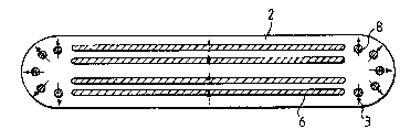
Figure 5 shows one example of a flat elongate
element according to this invention. At the central
20 part of the cross-section the element has flat bismuth
oxide bodies 6, and at both side parts of the cross-
section, thallium oxide superconductor wire bodies 8
are used. ~ecause their perfrrm~nrP is relatively
i nr~errntlrnt of the direction of magnetic ~lux, the
25 thallium oxide wires 8 were located at the sides for
optimum magnetic field distribution, while the bismuth
27 2049433
oxide bodies 6 which are sensitive to the direction of
magnetic flux were positioned at the centre. Thus, the
material of the superconductive element is not
nt:~:c:s:,~ily limited to only one kind, but any desired
5 combination of ~u~ ductivQ materials h~ay be chosen
according to the magnetic field distribution.
Figures 6(a) to 6(e) illustrate a process of
making the product of Figure 5 according to this
invention. In this embodiment, a multicore element of
lO Figure 6 ( a ) similar to that of Fig . 1 r but with ten
core wires, is divided in two ( b ); a plurality of f lat
superconductor tapes with metal rlA~9~9;n~, one of which
is shown at ( c ), are stacked together as shown at ( d );
this stack and the divided elements o~ ( b ) are loaded
15 into a prefabricated silver tube 20 as illustrated at
( e ); and the assembled wire rod is then rolled to
produce the desired element of Figure 5.
As shown in Figure 7, it is possible to stack
multiple flat superconductive rn~rnn~nt wires 10 of the
20 shape o~ Figure 6(c). In this case, the crystal
orientations of each superconductive component wire ( c-
axis Al ~, t of crystals in each superconductive
component wire ) are normal to the longitudinal
direction of the wire, }:ut the crystal Al; ' nts 3 in
25 a plane crossing the longitudinal direction at right
angles are shifted sliyhtly from each other, producing
28 2049433
a similar overall effect to that obtained when the
crystals are randomly oriented, although in this case
the range of angular distrlbution is less. This
restricted range of ~l i," t directions of the c-axes
5 is not a problem, when forming a coil, if the element
of Figure ~ is placed back-to-back with another
identical element.
Figure 8 shows one example of the product
according to this invention in which a ceramic body
10 ( MgO ) of polygonal cross-section is used as a
substrate. In this example, a sintered MgO rod 12 with
octagonal cross-section has attached to it
Bil 6 Pbo 4 Sr2 Ca2 CU3 l o superconductive component bodies
14 on the surface in such a manner that the c-axis
15 iil;~n~^nt direction 6 of the oxide crystals on each
face is perp~n~ r to that face of the substrate.
A process of making the wire product of Figure 8
using a thallium oxide will be described. A
polycrystalline MgO rod ( 20 mm across and 400 mm long )
20 was worked into a rod 12 of regular polygonal cross-
section. Then, on the surface of this rod was formed a
thallium oxide superconductive film by sputtering. The
film was annealed in air at 830C for 30 hours. The
critical temperature measured was 125 ~. X-ray
25 diffraction inspection revealed that the crystal c-
axes are oriented in a direction normal to each side of
29 2049433
the rod. E~amination of directional vari2tions o E the
c-axes using maximum point mapping showed that the
orientation deviation is within 2. In a magnetic
field of l tesla ( T ), this wire product has a critical
5 current value of more than 10 A and a critical current
density Jc of 10~ to 105 A/cm2 . The critical current
density ~c e~hibited almost no change when the wire
product was rotated in the plane of its cross-section.
Figures 9 and 10 show other examples of flat
10 wire products, which differ from the product of Figure
5 in terms of the c-axis directions of ;~ n~-nt. In
Figure 9, twelve f lat superconductive component wires
16 are arranged as shown at each side portion of the
flattened wire product to reduce the effect of non-
15 uniform magnetic field distribution at the sides of theelement. At the central region, ~lat superconductive
wires 17 are arranged parallel to each other. The c-
axes of each superconductive core wire 16,17 are normal
to the flat surface.
In Figure 10, the c-axis crystal ~ t
directions ( which are perpendicular to the longitudinal
direction of the element) of the flat superconductive
core wires 18 are randomly distributed in the cross-
section of the flattened wire product. To make this
embocliment, a silver bar ( 100 mm across and 200 mm
long ) is formed with a plurality of flat holes each
30 2C49433
measuring 10 mm wide and 3 mm thick by discharge
~-^hi ni nS, The flat surfaces of the holes are directed
randomly. Thallium oxide superconductive powder, which
has been prepared beforehand, is filled into the holes
5 in the round silver bar. The bar is then drawn into a
wire rod 2 . 8 mm in outer diameter and 2-5 m in length.
After each 25~6 reduction, the drawn wire is z~nn~ ri at
400C for 30 minutes. The drawn wire is heat-treated
at 835C for 200 hours. After this long heat
10 treatment, the a-b planes of crystals of superconductor
have grown parallel to the flat boundary surface
between the superconductor and the silver.
Addition in trace amounts of compounds, such as
PbO, K2 or K2 C03, which help promote the crystal
15 growth, to the filling powder, accompanied by heat
treatment at 650-850C for 5-100 hours, improves the
alignment of the crystals. When the ratio of the
amounts of elements is 2:2:2:2:x for Tl:Ba:Ca:Cu: (K or
Pb ), x is preferably 0 . 05-0 . 5 . The crystal grain size
20 can be more than 10 times greater than when such
compounds are not added.
Figure 11 shows another embodiment of a product
according to this invention The cross-sectional
structure of the product is r~ r~~ r and has annular
25 superconductor oxide layers 21 and metal layers 20
alternately The c-axes of the oxide crystals are all
32 2049433 -
axis of the element and the a-b planes of crystals are
oriented in the longitudinal direction.
Figure 14 illustrates a cross-sectional ~Lu~;LuL~:
of an element similar to that of Figure 13 but with the
5 outer diameter formed as a hexagon and the spirally
coiled core 26 ' having six flat sides in each turn of
the spiral. The crystal c-axes of the wire 26 ' are
almost completely normal to the outer sides of the
metal layer 25 ', as indicated by arrows 3.
While the superconductive core 26 ' in Figure 14
is wound spirally, the element of Figure 15 has
multiple polygonal layers 21 ' as in Figure 11 but with
a hexagonal cross-section. In this case, the
directions normal to the outer sides of the metal
15 layer 20 ' strictly agree with the directions of crystal
c-axes of the respective portions of the core layers
21' .
We have shown some embodlments of wire products
and their cross-sectional structures in the foregoing.
20 The regular polygon cross-section referred to in these
embodiments means polygons with f our or more angles but
preferably not more than 20 angles
An example of an element of the invention which
uses a plurality of the products described above as
25 components is shown in Figure 16 which shows a
multicore ele~ent, in which seven component elements 29
31 2049433
in the radial direction relative to the axis of the
element and the a-b planes of the crystal5 are aligned
in the longitudinal direction.
Figure 12 also shows another ,y LL lcal layered
cross-sectional structure of an element of this
invention, similar to Figure 11. The cross-sectional
shape of the element and each superconductive layer 24
is a regular polygon to enhance the ~ t of the
crystals in each side of the polygon. In this
example, the element has an octagonal cross-section and
the radial thickness of the oxide superconductor layers
24 is 0.1 ,um to 0.1 mm because in this range of
thickness a suf f icient amount of current can easily be
passed. This tl~ .kn~cs is desirably in the range of 1
to 20 ,um. The crystal orientation of each ring-
shaped core wire 24 varies around the polygon, with the
crystal c-axes in each side extending normal to the
side, i.e. approximately radially relative to the
centre axis
Figure 13 shows stlll another layered cross-
sectional structure of an element of this invention,
similar to Figure 11 It differs from Figure 11 in
that a single core body 26 is embedded spirally coiled
in the metal matrix 25. The c-axes oi the oxide
superconductor crystals are at all points directed
parallel to the radial direction relative to the centre
2049433
33
each with the cross-sectional structure of Figure 1 are
~mh~ in a metal matrix 28: It is also pnsC; h~ ~
for example to form products which have seven elements
with the cross-section of Figure 14 or seven ~1 3~ t:,
with the cross-section of Figure 15.
In these cases, the metal t~l ar~ n~ material used
is silver and the outermost layer may be coated with a
nickel oxide insulating layer. The nickel oxide
insulating layer on the outer surface of the product
may ~e iormed by first coating the outermost layer of
the metal pipe with nickel and n~ ; 7i n~ the nickel
layér during the f inal heat treatment .
One example of a process of fabricating a multi-
component product according to this invention is shown
in Figure 17. A superconductor powder 30 ~ in this
em~1odiment Bi~ ~ Pbo ~ Sr2 Ca2 CU3 10 ) which was produced
by conventional solidus reaction method is filled into
a silver pipe 31, lO mm in outer diameter, 7 mm in inner
diameter and 500 mm in length. This is drawn by a draw
bench into a wire 5 mm in outer diameter and is further _~
worked into a thin tape wire 32 0.15 mm thick by a
rolling mill. After this tape wire 32 is heat-treated
at 845 C for 100 hours, it is coiled in the direction
of its transverse cross-section i e. around a
longitudinal axis. The coiled tape 33 is ~urther
worked into a wire 34 of hex~gonal cross-section by a
34 2049433
hexagon die. The wire 34 measures 2. 8 mm along a
diagonal line of the hexagonal cross-section and is 1-2
m in length This core wire 34 is inserted into holes
36 in a silver rod 35 that are ormed to the same shape
5 and dimension as the core wire. The rod loaded with
core wires is drawn again into a wire 2 mm in outer
diameter, which i5 then heat-treated at 845C for 100
hours When the product is to be f ormed into a coil,
it is coiled before being subjected to this ~inal heat
10 treatment. The thickness of the superconductor cores
in the iinal wire product is 0 .1 um to 0 . 2 mm depending
on the degree to which the wire is drawn.
Next, a process o fabricating an element with
the layered structure according to this invention as
15 shown in Figures ll, 12 and 15 will be Prrl ~;nPd by
Figure 18. A superconductor powder 3Q (in this
embodiment Tl2 Ba2 Ca2 CU3 l ~ ) which was produced by a
conventional solidus reaction method is filled into a
silver pipe 31.10 mm in outer diameter, 8 mm in inner
20 diameter and 400 mm in length. At this time, a silver
rod 37 5 mm across is inserted at the centre of the
silver pipe 31. The S~lrprron~ tor powder is uniformly
filled into the gap between the silver bar and the
silver pipe. This composite rod is drawn by a draw
25 bench into a wire 5 mm across. The drawn wire is
inserted into another silver pipe 38~10 mm in outer
3s 2049433
diameter, 8 mm in inner diameter and 400 mm in length.
Superconductive powder 39 is 1ûaded into the gap
between the pipe 38 and the wire. This process is
repeated to form a multilaye~ed element.
Using a hexagon die, the element is worked into a
hexagonal cross-section of side length 1. 4 mm. Forming
a multiple element with multiple components as well as
coiling may be done in the same way as described in
Figure 17.
The ~h~ r~kn~cc of the superconductive core layers
in the final product is 0.1 ,um to 0.1 mm. It was found
that the crystal orientation becomes better ~s the core
thickness gets smaller. The final heat treatment was
pt:L~U d at 845C for 100 hours.
Figure l9 shows the relationship between the
angle subtended by the crystal a-~ plane in a wire
product and the magnetic field and the critical current
density Jc, for several products of this invention and
a previously known product. The critical current
density was measured by the dc 4-~rmin;~l resistance
method, which uses a current value when 1 ,uV is
generated between voltage 1-~rmini~l c and calculated from
cross-sectional area of the oxide superconductor
element .
This measurement was taken in licluid nitrogen ~77
K ) at the external magnetic field of lT . The
2049433
36
directions of current and magnetic f lux were
perp~nrlic- l~r to each other.
~he lines in Figure 19 relate to products as
f ollows: -
12 . . . product of the invention ( Fig. 15 )
13 . . . product of the invention ( Fig. 10 )
14 . . . product of the invention ( Fig. 5 )
15 .......... known product for comparison having a
cross-sectional structure as shown in Fig. 10, but in
10 the plane perpendicular to the longitudinal direction,
the oxide crystals are oriented in one direction only.
From Figure l9, it is seen that the products of
this invention have relatively small or very small
dependency of Jc on the direction of magnetic field.
15 On the other hand, the known product cannot pass a
superconducting current when the angle between the a-b
crystal plane and the magnetic flux approaches 20.
With the product of this invention, however, the
critical current density is as high as 103 A/cml or
20 more. Particularly with the elements of this invention
corresponding to lines 12, 13 of Figure 19, in which
the crystals are oriented isotropically, the fall in
the critical current density due to variation of the
angle is small. ~he element of line 13 in which
25 crystal alignment directions of the core wires are
oriented completely at random shows no change in the
37 2049433
critical current density.
The present invention is ~nrPrnP~ with the
element structure and does not place particular
limitations on the :,U~t:L~ULldUCtlng oxide material used.
5 In the following, we list materials which have been
found by experiment to have similar effects as those of
the preceding embodiments.
Table 1 lists some of the currently known maj or
superconductive oxides. The present i~lve:~lLol~, using
these materials ~ made elements of hexagonal cross- =
section by the fabrication procedure shown in Figure
18 .
These Pl ~:, were heat-treated under the known
optimum conditions. As a result, the elements of
15 hexagonal cross-section exhibited almost the same
critical temperatures Tc as the corresponding bulk
materials. These results are shown in the following
Table, together with results of tests of critical
current density of the elements at temperatures of 4 . 2
20 K and 77 K, as indicated. The critical current densit-y
at these temperatures with no magnetic iield applied is
Jco. The critical current density Jc was measured with
a magnetic f ield of lT applied and at two mutually
perpPn~ orientations of the element in the
25 magnetic field (~=0 and ~gO ) . The directions of
magnetic field and current were perppnr~ ~ to each
38 2049433
other. The results indicate that the fall in the
critical current density Jc in the magnetic field
relative to the value at no field is constant at about
on--thl~d o~ th Jco velue.
-- 39 --
~ Tl~sL 2 0 4 9 4 3 3
.
,~
~ ~, ~ ~ ~ , ~. ~ . ~ ~ r r r r' r r ~ r r r r r r r
cO~
Q ' o C o o o o o o o o o o o o o o o o o o o o o o o o
O n o ~ G o c n _~ n o o = = o ~ ~ ~ n r~
oQ o o o o o O o o o o o a o = o O O O O O O O O o o o
-
D ~1
J, I o~ n r = = 6,~ r = = = ~ = _ ~ O ~ r = c ~: ~`I r ~ o c r
U. c
~,
1~
n = r,~ = = I~ rl O ~ _ ~ r `~ "1 r r r
c
_ ~ _ _ c = ~ .
- ~J 2~ t~ n ~ r
- O ~10 0 0 _ ~ D ' r 6 ' ~ O O
OG rJD r~D 2= ~ r r r ~ ~ , r r
_ _ _ _ ~ _ r _ ~ ~ o o
-- -- ~ r r r ~ - ~ t
C o _~ ~ n ~ n 8 r = o _ ~ r~
2 ~ n 8 r G =
~pFxO ~p}xo ~p}xo ~p~xo =n}Te~
mueq~Oe~T =n}~ ; q~nulS}~I
2049433
Figure 20 is a partly cutaway view of a solenoid
coil using a multi-~ ~ ent element 46, which consists
of seven Pl ~:j as shown in Figure 12. A core
5 cylinder 47 of the coil is an alumina cylinder. During
the coiling operation, it is important to take care so
that the directional relationship between the element
a-b plane crystal orientation and the core cylinder
does not change. ~he direction o the crystal
10 orientation in each element may be marked at many parts
on the element surface, if nPsPgsRry.
Figure 21 shows one example of a double pancake
coil using a multicore element 48 as sho~n in Figure 5.
The coil has six layers of windings 49 of the elements
15 48 in which the long faces of the elements 48 are
parallel to the coil axis. The turns in each winding
49 are separated by insulation 50 in the f orm of non-
woven alumina fabric. The windings 49 are separated by
alumina spacer plates 51 and are connected in series by
20 outside electrodes 52 of silver and coil cores 53 also
of silver.
The coil o Figure 20 ~enerated a magnetic f ield
of 0 . lT at 77K, while the coil o Figure 21 produced a
magnetic field of lT at 77K. The magnetic ield
25 intensity gener~ted by the coil depends on the number
of turns of the wind~ngs, density of the windings, ~nd
41 2049433
cuIrent. When these parameters are optimized, it is
possible to produce a 8tronger f ield .
With this invention it is thus possi~le to
provide superconductive ~1~ L~ and coils thereof
5 which have critical current densities at a licluid
nitrogen temperature, let alone at a liguid helium
temperature, and which have little dependence on the
direction of the magnetic flux in strong magnetic
f ields .
-