Language selection

Search

Patent 2049582 Summary

Third-party information liability

Some of the information on this Web page has been provided by external sources. The Government of Canada is not responsible for the accuracy, reliability or currency of the information supplied by external sources. Users wishing to rely upon this information should consult directly with the source of the information. Content provided by external sources is not subject to official languages, privacy and accessibility requirements.

Claims and Abstract availability

Any discrepancies in the text and image of the Claims and Abstract are due to differing posting times. Text of the Claims and Abstract are posted:

  • At the time the application is open to public inspection;
  • At the time of issue of the patent (grant).
(12) Patent Application: (11) CA 2049582
(54) English Title: FREQUENCY SYNTHESIZER WITH A PHASE-LOCKED LOOP WITH MULTIPLE FRACTIONAL DIVISION
(54) French Title: SYNTHETISEUR DE FREQUENCE COMPORTANT UNE BOUCLE A VERROUILLAGE DE PHASE AVEC DIVISION FRACTIONNAIRE MULTIPLE
Status: Deemed Abandoned and Beyond the Period of Reinstatement - Pending Response to Notice of Disregarded Communication
Bibliographic Data
(51) International Patent Classification (IPC):
  • H03L 07/18 (2006.01)
  • H03K 23/66 (2006.01)
  • H03K 23/68 (2006.01)
  • H03L 07/197 (2006.01)
(72) Inventors :
  • BRUNET, ELIE (France)
  • DE GOUY, JEAN-LUC (France)
  • GINESTET, THIERRY (France)
(73) Owners :
  • THOMSON TRT DEFENSE
(71) Applicants :
  • THOMSON TRT DEFENSE (France)
(74) Agent: ROBIC AGENCE PI S.E.C./ROBIC IP AGENCY LP
(74) Associate agent:
(45) Issued:
(22) Filed Date: 1991-08-20
(41) Open to Public Inspection: 1997-10-12
Availability of licence: N/A
Dedicated to the Public: N/A
(25) Language of filing: English

Patent Cooperation Treaty (PCT): No

(30) Application Priority Data:
Application No. Country/Territory Date
90 10 512 (France) 1990-08-21

Abstracts

English Abstract


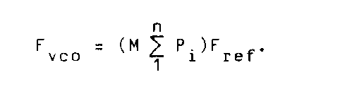
A frequency synthesizer comprises a single phase-locked
loop controlled by a reference clock formed by a voltage-controlled
oscillator, a programmable divider with variable
division rank M, a phase detector, and a loop filter. It
also comprises a predetermined number n of fractional division
structures, each implementing a frequency step P i x
F ref lower than the reference frequency F ref. Each fractional
structure is coupled in parallel with said programmable
divider to add to said division rank M fractional increments
P i such that the ratio between the frequency F vco provided
by said oscillator and said reference frequency be defined
as a function of said increments P i by the relationship :
(see fig. I)
Application : any type of product or system requiring a frequency
synthesizer, in particular communications system with
frequency agility.


Claims

Note: Claims are shown in the official language in which they were submitted.


- 8 -
Claims
What is claimed is :
1. A frequency synthesizer with a phase-locked loop with
multiple fractional division, of the type comprising a single
phase-locked loop controlled by a reference clock formed
by a voltage-controlled oscillator, a programmable divider
with variable division rank M, a phase detector, and a loop
filter, comprising in addition a predetermined number n of
fractional division structures, each implementing a frequency
step P i x F ref lower than the reference frequency F ref,
and wherein each fractional division structure is coupled
in parallel with said programmable divider to add to said
division rank M fractional increments P i such that the ratio
between the frequency F vco provided by said voltage-controlled
oscillator and said reference frequency F ref be defined
as a function of said increments P i by the relationship :
<IMG>
2. A synthesizer according to claim 1, wherein each of said
fractional division structures provides the product of said
reference frequency by a fractional number P i = a i/Q i, where
O < a i < Q i, the numbers Q i being relatively prime numbers.
3. A synthesizer according to claim 2, wherein said frequency
step is equal to said reference frequency divided
by the product of said numbers Q i.
4. A synthesizer according to claim 3, wherein each of said
n fractional division structures comprises a programmable
modulo-Q i divider with a variable division rank a i.

- 9 -
5. A synthesizer according to claim 4, wherein said division
rank M of said programmable divider of the single loop
is increased by one unit by each of said n fractional division
structures a i times every modulo Q i of each structure.

Description

Note: Descriptions are shown in the official language in which they were submitted.


CA 02049~82 1997-10-12
Frequency synthesizer with a phase-locked loop
with multiple fractional division
Background of the invention
The present invention relates to a frequency synthesizer
with a phase-locked loop with multiple fractional division.
A frequency synthesizer with a phase-locked loop compri-
ses conventionally in the manner described, for example,
in the book of U.L. Rhode entitled "Digital PLL frequency
Synthesizers - Theory and Design", 1983, Prentice Hall Inc.
Englewoods Cliffs, a voltage-controlled oscillator, a varia-
ble-modulo divider, a phase detector, clock providing a re-
ference frequency Fref, and possibly a loop filter. When
the loop is locked, if M denotes the value set for the divi-
der, the output frequency FVco from the voltage-controlled
oscillator is equal to M times the value of the reference
frequency Fref. When the value M set for the divider chan-
ges, the synthesized frequencies obtained change by steps
equal to the reference frequency F ef' within the operating
limits of the voltage-controlled oscillator.
To obtain a frequency synthesis step lower than Fref,
it is known to introduce a fractional division loop which
produces a frequency increment equal to a/Q times the refe-
rence frequency Fref, where Q is equal to the quotient ofthe reference frequency by the desired frequency step, where
0 < a < Q-1.
Through a digital phase accumulator system, the main
division ratio M is incremented by one unit, and this eachti-
mes every Q cycles of the reference frequency. The frequencystep is then equal to the reference frequency divided by Q.

CA 02049~82 1997-10-12
-- 2
The advantage of this approach is that for comparable
characteristics, the number of steps M to be set for the
divider is reduced and that the loop filter has a higher
cutoff frequency, which improves the response of the loop.
However, while the foregoing device is well suited to
frequency synthesis, it is not appropriate for the synthe-
sizers modulated in frequency or in phase from a modulation
introduced, for example, in the reference frequency, for
it appears that the maximum rate of this modulation is limi-
ted to low values. In addition, the synthesis frequency li-
nes which appear at the output of the voltage-controlled
oscillator and which are mainly due to the phase jitter of
the phase comparator have relatively high levels which give
to these synthesizers a relatively poor spectral purity.
However, when using not a single fractional division
structure, but two of them, as this is described in the
French patent application N~ 2 426 358 entitled "Synthéti-
seur de fréquence à division directe à pas après virgule",
it is possible to improve in a very significant manner the
spectral purity of the signals from the synthesizers with
fractional division.
However, for some applications, this improvement is not
sufficient, in particular it does not allow to use such syn-
thesizers in communications systems with fast frequency agi-
lity.
Summary of the invention
A purpose of the present invention is to remedy the abo-
ve-mentioned disadvantages.
To this end, an object of the present invention is a
frequency synthesizer with a phase-locked loop with multiple

CA 02049~82 1997-10-12
fractional division of the type comprising a single phase-
locked loop controlled by a reference clock and comprised
of a voltage-controlled oscillator, a programmable divider
with variable division rank M, a phase detector, and a loop
filter, characterized in that il also comprises a predeter-
mined number n of fractional division structures, each im-
plementing a fequency step Pi x Fref lower than the referen-
ce frequency Fref, and in that each fractional division struc-
re is coupled in parallel with the programmable divider to
1û add to the division rank M fractional increments Pi such
that the ratio between the frequency FVco provided by the
voltage-controlled oscillator and the reference frequency
Fref be defined as a function of the increments Pi by the
relationship :
n
vco 1 i ref
Brief description of the drawings
Other features and advantages of the present invention
will become apparent from the following detailed description
of preferred embodiments given as a non-limitative example
with reference to the accompanying drawings, in which :
- Figure 1 is a block diagram of a synthesizer according
to the present invention;
- Figure 2 shows the architecture of a synthesizer according
to the present invention capable of operating over a range
of frequencies extending from 225 MHz to 400 MHz;
- Figures 3A and 3B are circuit diagrams of two embodiments
of a fractional division loop for controlling a front divi-
der in Figure 2; and
- Figure 4 is a plot for comparing the theoretical level
of the frequency synthesis lines obtained with a single frac-
tional synthesis and with a multiple fractional synthesis.

- CA 02049~82 1997-10-12 ".
Description of the preferred embodiments
The synthesizer according to the present invention which
is shown in Figure 1 comprises a single phase-locked loop
composed of a voltage-controlled oscillator 1, a programma-
ble divider with variable division rank M 2, a phase detec-
tor 3, and a loop filter 4, all these elements being casca-
ded in this order. A reference clock 5 providing a reference
frequency Fref supplies the phase detector 3 to determine,
when the loop is locked to the proper frequency, the phase
deviation between the signal provided by the clock 5 and
the signal provided by the divider 2. It also comprises n
fractional division structures 61~ ..., 6i through 6n, each
of which implements a frequency step lower than the referen-
ce frequency F f~ of the form (a/Q)Fref, where Q is equal
to the quotient of the reference frequency by the desired
frequency step, and a is an integer such that 0 < a < Q-1.
By choosing for each fractional division numbers Q1'
Q2' ' Qi' ~ Qn relatively prime two by two, and a1,
20 ... ..., an such that :
O < a1 < Q1-1
O < a2 < Q2-1
......
0 < an < Qn~1'
the synthesizer shown in Figure 1 allows to perform the syn-
thesis of frequencies FVco such that :
( a1 a2 l + ... + Qn)Fref = (M+~ Pi)Fref,
where Pi = ai/Qi

CA 02049~82 1997-10-12 '.
with a frequency step equal to the quotient of the reference
frequency Fref by the product of the prime numbers Q1~ Q2'
' Qn. Under these conditions, the divider 2 is incremen-
ted by one unit a1 times every Q1 reference cycles, a2 times
5 every Q2 reference cycles, , ai times every Qi reference
cycles, and an times every Qn reference cycles.
The advantage of this approach is that it provides a
significant improvement of the level of the frequency lines
about the output frequency of the synthesizer with respect
to all known synthesis devices with fractional division of
the prior art. In the example of application of the fore-
going principle to the implementation of a synthesizer allo-
wing to cover a frequency band between 225 and 400 MHz shown
in Figure 2, where the elements corresponding to those of
Figure 1 are denoted by the same reference numerals, the
number of fractional division structures 61 through 64 is
limited to 4, and the variable-rank divider 2 is composed
of a front divider 21 and a tail divider 22. In contrast
with Figure 1, the synthesizer includes a multiply-by-four
circuit 7 between the oscillator 1 and the divider 2.
In this example, the reference frequency Fref = 10.5 MHz.
The front divider 21 is a variable divider whose division
ratio is adjustable by applying a 0 or a 1 to each of its
four inputs.
Each element 61 through 64 is formed by an adder modulo
an integer Qi' which is programmable by integers ai < Qi.
In the above example, the modulos Qi of the adders 61
through 64 have respectively the values Q1 = 3' Q2 = 4' Q3 =
5 and Q4 = 7, which are relatively prime numbers.
The frequency step is then of :
10.5 MHz/(3x4x5x7) = 25 kHz
at the output of the multiply-by-four circuit 7 and conse-
quently of 6.25 kHz for the oscillator 1.

- CA 02049~82 1997-10-12 "
Applying the relationship (1) gives :
F f/Q1 = 3.5 MHz;
Fref/Q2 = 2.625 MHz;
Fref/Q3 = 2.1 MHz; and
F f/Q4 = 1.5 MHz.
1 0
The lowest frequency synthesis step, that is, 25 kHz
at the output of the multiply-by-four circuit 7 (6.25 kHz
at the outputof the oscillator 1) is obtained by performing
the operation :
ref 2 ( ref/Q3) +2(Fref/Q1) + 2(F f/Q4) - 2F
that is :
1x2.625MHz + 4x2.1MHz + 2x3.5MHz + 2x1.5MHz - 21MHz = 25 kHz.
Examplary embodiments of the adders 0, 1, 2 modulo 3
and 0, 1, ..., 6 modulo 7 for the implementation of the ad-
ders 61 through 64 are shown in Figures 3A and 3B. They com-
prise adder circuits 81 through 84 of the type of those knownunder the reference number 74F283 marketed by National Semi-
conductor and Motorola. These circuits are programmed by
the numbers ai by means of logical interface circuits 91
and 92. Registers 1~1 and 1~2 placed at the output of the
divider circuits 82 and 84, respectively, allows to store
at each increment of the reference frequency Fref the state
of the divider to increase it by the value ai at the next
increment.
The plot in Figure 4 illustrates the spectral purity

- CA 02049~82 1997-10-12 ".
obtained with a synthesizer with multiple fractional synthe-
sis of the type shown in Figure 2 as compared to that which
can be obtained with a simple fractional synthesizer. This
graph shows that for the modulos Q1 = 3' Q2 = 4' Q3 = 5'
Q4 = 7, and a frequency step PSyn = 25 kHz leading to a re-
ference frequency Fref = 10.5 MHz, the theoretical level
of the lines about the synthesized carrier frequency drops
successively by 40 dB a first time for F1 = Q1xQ2xQ3xP
= 1.5 MHz, a second time for F2 = Q1XQ2xpsyn = 300 kHz, a
third time for F3 = Q1xPsyn = 75 kHz, and finally a fourth
time for F4 = PSyn = 25 kHz. With a synthesis frequency band
with single fractional division, the level of the lines bet-
ween the frequency step of 25 kHz and the synthesized car-
rier frequency remains at 0 d8, whereas with the loop shown
in Figure 2, the latter drops suddenly by 40 dB as soon as
the frequency reaches 1.5 MHz.

Representative Drawing
A single figure which represents the drawing illustrating the invention.
Administrative Status

2024-08-01:As part of the Next Generation Patents (NGP) transition, the Canadian Patents Database (CPD) now contains a more detailed Event History, which replicates the Event Log of our new back-office solution.

Please note that "Inactive:" events refers to events no longer in use in our new back-office solution.

For a clearer understanding of the status of the application/patent presented on this page, the site Disclaimer , as well as the definitions for Patent , Event History , Maintenance Fee  and Payment History  should be consulted.

Event History

Description Date
Inactive: IPC from MCD 2006-03-11
Inactive: Cover page published 2000-12-20
Deemed Abandoned - Failure to Respond to Maintenance Fee Notice 1999-08-20
Application Not Reinstated by Deadline 1999-08-20
Inactive: Dead - RFE never made 1999-08-20
Inactive: Abandon-RFE+Late fee unpaid-Correspondence sent 1998-08-20
Inactive: IPC assigned 1997-12-29
Classification Modified 1997-12-29
Inactive: First IPC assigned 1997-12-29
Inactive: Delete abandonment 1997-10-16
Application Published (Open to Public Inspection) 1997-10-12
Inactive: Adhoc Request Documented 1997-10-10
Inactive: Adhoc Request Documented 1997-10-08
Inactive: Delete abandonment 1997-10-08
Deemed Abandoned - Failure to Respond to Maintenance Fee Notice 1997-08-20
Deemed Abandoned - Failure to Respond to Maintenance Fee Notice 1996-08-20
Deemed Abandoned - Failure to Respond to Maintenance Fee Notice 1995-08-21
Deemed Abandoned - Failure to Respond to Maintenance Fee Notice 1994-08-22
Time Limit for Reversal Expired 1994-08-22
Deemed Abandoned - Failure to Respond to Maintenance Fee Notice 1993-08-20

Abandonment History

Abandonment Date Reason Reinstatement Date
1999-08-20
1997-08-20
1996-08-20
1995-08-21
1994-08-22
1993-08-20

Maintenance Fee

The last payment was received on 1998-07-14

Note : If the full payment has not been received on or before the date indicated, a further fee may be required which may be one of the following

  • the reinstatement fee;
  • the late payment fee; or
  • additional fee to reverse deemed expiry.

Patent fees are adjusted on the 1st of January every year. The amounts above are the current amounts if received by December 31 of the current year.
Please refer to the CIPO Patent Fees web page to see all current fee amounts.

Fee History

Fee Type Anniversary Year Due Date Paid Date
Registration of a document 1991-11-25
MF (application, 2nd anniv.) - standard 02 1993-08-20 1993-07-16
MF (application, 3rd anniv.) - standard 03 1994-08-22 1994-07-15
MF (application, 4th anniv.) - standard 04 1995-08-21 1995-07-26
MF (application, 5th anniv.) - standard 05 1996-08-20 1996-07-24
MF (application, 6th anniv.) - standard 06 1997-08-20 1997-07-15
MF (application, 7th anniv.) - standard 07 1998-08-20 1998-07-14
Owners on Record

Note: Records showing the ownership history in alphabetical order.

Current Owners on Record
THOMSON TRT DEFENSE
Past Owners on Record
ELIE BRUNET
JEAN-LUC DE GOUY
THIERRY GINESTET
Past Owners that do not appear in the "Owners on Record" listing will appear in other documentation within the application.
Documents

To view selected files, please enter reCAPTCHA code :


To view images, click a link in the Document Description column. To download the documents, select one or more checkboxes in the first column and then click the "Download Selected in PDF format (Zip Archive)" or the "Download Selected as Single PDF" button.

List of published and non-published patent-specific documents on the CPD .

If you have any difficulty accessing content, you can call the Client Service Centre at 1-866-997-1936 or send them an e-mail at CIPO Client Service Centre.


Document
Description 
Date
(yyyy-mm-dd) 
Number of pages   Size of Image (KB) 
Abstract 1997-10-11 1 22
Description 1997-10-11 7 211
Claims 1997-10-11 2 37
Drawings 1997-10-11 3 59
Representative drawing 1999-03-03 1 4
Representative drawing 1999-06-15 1 1
Representative drawing 2000-11-29 1 1
Reminder of maintenance fee due 1997-09-27 1 111
Reminder - Request for Examination 1998-04-20 1 117
Courtesy - Abandonment Letter (Request for Examination) 1998-09-30 1 171
Courtesy - Abandonment Letter (Maintenance Fee) 1999-09-19 1 187
Fees 1996-07-23 9 294
Fees 1997-07-14 3 99
Fees 1994-10-02 1 16
Fees 1993-07-15 2 65
Fees 1994-07-14 2 57