Note: Descriptions are shown in the official language in which they were submitted.
~~~~~~3~
sp~cIFICATZOrr
B.B. ackaround of the Invention
The present invention is directed generally to
circuit monitoring devices, and more particularly, to an
improved high im~5edance voltage indicator.
Various devices have been developed for indicating
the voltage level on electrical conductors in high voltage
power distribution systems.
One such early device was an electroscope wherein a
pivoted vane was arranged to be repelled from a fixed vane on
contact with an energized line. This device had to be
positioned very precisely since the force of electrostatic
repulsion of the vanes was relatively small and opposed by
gravity. Another early device utilized an electromechanical
meter movement in conjunction with a high resistance series
resistor to ground. This device was cumbersome, and could
not detect small charges and at high voltages required a high
potential impedance return path to ground.
The present invention overcomes these drawbacks by
providing a voltage indicator which incorporates a high
impedance non-mechanical visual display device in the form of
a liquid crystal display, This results in an indicator of
increased sensitivity which is more compact and easier to
manufacture, and which provides a large non-ambiguous
indication of voltage level to the user.
Accordingly, it is a general object of the present
invention to provide a new and improved voltage indicator.
1
Tt is a more specific object of the present
invention to provide a voltage indicator which avoids the use
of electromechanical indicator mec;hanisms and batteries.
It is a still more specific object of the invention
to provide a voltage indicator wh~.ch is more compact and less
costly to manufacture,
Summary of the InvPn~i~r
The invention, is directed to a voltage indicator
for indicating the voltage level on a monitored electrical
conductor. The indicator includes a housing adapted for
mounting in a fixed position relative to the monitored
conductor, voltage indicating means within the housing
comprising a plurality of high impedance display devices each
having at least one pair of display electrodes disposed in
operative association with a layer of voltage-responsive
light eontro111ng material, and each providing on the
exterior of the housing a first display condition in the
absence of an actuating signal exceeding a pre- determined
voltage level applied to the display electrodes, and a second
display condition in the presence of an actuating signal
exceeding the predetermined voltage level applied to the
display electrodes, and circuit means comprising a voltage
divider for applying progressively increasing portions of the
voltage on the monitored conductor to respective ones of the
display electrodes of the display devices to actuate the
display devices to the second display condition in a
predetermined sequence with increasing voltage on the
2
'~ i
~~~~' c~ D
monitored conductor.
Brief Description of the Drawings
The features of the present invention which are
believed to be novel are set forth with particularity in the
appended claims. The invention, together with the further
objects and advantages thereof, may best be understood by
reference to the following description taken in can~unction
with the accompanying drawings, in the several figures of
which like reference numerals identify like elements, and in
which:
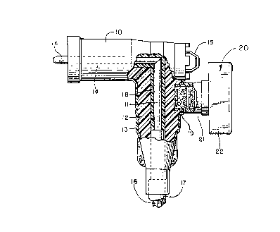
Figure 1 is a side elevational view partially in
section of a voltage indicator constructed in accordance with
the invention shown installed on the test paint terminal of
an elbow terminator.
Figure 2 is a front elevational view of the
installed voltage indicator of Figure 1.
Figure 3 is a front elevational view showing the
indicator window of the voltage indicator of Figures 1 and 2)
Figure 4 is an enlarged cross-sectional view of the
voltage indicator taken along line 4-~ of Figure 3.
Figure 5 is a cross-sectional view of the voltage
indicator taken along line 5-S of Figure 4.
Figure 6 is an enlarged crass-sectional view of the
votlage indicator taken along line 6-6 of Figure S.
2S Figure J is an enlarged cross-sectional view of a
portion of the vot:lage indicator taken along line 7-7 of
Figure 6.
3
Figure 8 is an enlarged expladed perspective view
showing the principal elements of the liquid crystal display
component utilized in the voltage indicator of Figures 1-7.
Figure 9 is an electrical schematic diagram of the
voltage indicator of Figures 1-8.
Figures 10A and 10B are front views of alternate
constructions of the voltage indicator for providing a
differential voltage indication.
Figure 11 is an interior cross-sectional view of
the differential voltage indicator of Figures 10A and 10B
showing principal electrical components thereof.
Figure 12 is an electrical schematic diagram of the
differential voltage indicator of Figures 10-11.
Description of the Preferred Embodiment
~teferring to the drawings, and particularly to
Figures 1-8, a plug-in type elbow connector for use in high
voltage alternating current power distribution systems for
establishing a plug-in connection to a transformer or other
system component (not shown) is identified generally by
reference numeral l0. As shown, the connector 10 includes
generally a conductor 11 extending generally axially through
an electrically non-conductive body portion 12 encased in an
electrically-conductive sheath 13, the sheath being grounded
in accordance with conventional practice. An electrically-
conductive contact member 14 extends from conductor 11 to
mate with a complementary contact on the associated system
component. An areuate member 15 having ends anchored in the
4
.~Jvi~~
conductive sheath 13 extends from i:he connector to receive
the hooked end of a lineman°s tool (not shown). The axial
conductor 11 is connected, in accordance with conventional
practice, to the conductor 16 of a flexible cable 1"1 of the
type commonly utilized in power di.~tribution systems. A
layer 18 of semi-conductive material may be provided around
conductor 11 to provide stress relief for the electric field
within the connector in a manner well known to the art.
To provide for detecting fault currents or
measuring voltage levels in conductor 11 connector 10
includes a test point socket 19 for receiving a circuit
monitoring component, in this instance a voltage indicator
20) The test point socket 19, which is preferably
constructed as described in U.s) Letters Patent 4,904,932 of
the present applicant, is formed within the insulating body
portion of the connector, extending through the electrically-
conductive outer sheath 13. In nar~~r_mi~,._ m.h~~ ~~...°...L ~_
preferably cylindrical in form and of an axial extent such
that the test point socket 19 receives a portion of the fault
indicator housing)
The voltage indicator 20 is seen in Figures 3-5 to
include a stem portion 21 formed of an electrically
conductive rubber or similar semi-resilient material, and a
generally rectangular body portion 22 formed of a non-
electrically conductive impact resistant plastic or epoxy
material within which the principal electrical components of
the fault indicator are contained. In particular, within
5
!" f~ f, ( ~.
<3;~a~i~:9
housing portion 22 the fault indicator module includes a
rectangular insulator board 23 (Figures 4 and 5) positioned
perpendicularly to the axis of the housing at a location
intermediate the ends thereof, and ;a portion 24 (Figure 4) o:~
high electrical resistance potting compound at the inside end
of the housing far securing the insulator board in place.
Additional electrical components contained in housing 22
include a capacitive coupling element in the form of a
metallic plate 25 for capacitively coupling the circuitry of
the fault indicator to conductor 11, an electrically
conductive stem 26 for securing plate 25, a high impedance
electronic display component 27 for visually indicating
voltage level, and an arrangement 28 of coaxial wire segments
comprising a voltage divider for applying predetermined
portions of the voltage sensed on conductor 11 to display
device 27.
Operating power for the circuitry of voltage
indicator module 20 is derived from conductor 11 by means of
the metallic plate 25, which when indicator 20 is seated in
test point socket 19 is sufficiently closely spaced to the
conductor to provide a level of capacitive coupling whereby
an adequate alternating voltage is derived from the
conductor. A necessary ground return for this circuitry may
be provided, as shown in Figures 1-5, by an electrical ground
terminal 29 which is imbedded in housing portion 21.
When housing port~.on 21 is seated in test point socket 19 of
connector i0 conductor 29 is brought into electrical
6
_, i
~~~~'~i~~3
communication with the electrically grounded sheath 13 of the
connector.
As shown in Figures 3-5, 'within housing portion 22
the liquid crystal display component 27 is positioned against
a transparent window 30 such that the indicator face of the
component is readily viewable from the exterior of the
housing. A mask 31 Figure 4) formed of a thin sheet of
opaque material may be provided on the inside surface of
window 30 so that only the indicator face can be seen.
As shown in Figure 3, the liquid crystal display
component 27 is capable~of producing a vertical bar display
33 to indicate the voltage level in conductor 11. Indicia 34
on housing portion 22 beside window 30 assist the user in
quantifying the displayed level in volts or other units of
measure.
In the illustrated embodiment, where the bar graph
display is composed of six display elements, electrical
connections are made to display component 27 by means of six
electrically conductive terminals 35a-35f (Figure 6) arranged
along the top edge of the component.
Internally, as shown in Figure 8, the liquid
crystal display component 27 generally includes a transparent
face plate 40, a front polarizer 42,~a glass plate 43 on
which a transparent bacDcplane electrode 44 is provided, a
perimeter seal 46 containing a layer 47 of twisted nematic
liquid crystal material, electrically conductive edge
contacts 48, a glass~plate 4~ on which six transparent
7
indicator segment electrodes 50a-50f (plates 50c-50f not
shown) are contained, a rear polar~.s~er 52 aligned at right
angles to front polarizes 42, a ref:Lector 53 and a rear
support plate 54)
Display component 27 may be conventional in con-
struction and operation. The individual bar displays are
formed by the nematic liquid crystal layer 47, which in the
absence of an applied electric field has the property of
rotating the polarization of light as it passes through the
molecular layers of the layer, In particular, as randomly
polarized light enters the display component through face
plate 40, only vertically polarized light passes through
front polarizes 42. In the absence of an applied electric
field, the polarization of this polarized light is rotated
90o as it passes through the nematic liquid crystal layer 47
and reaches rear polarizes 50. Since the polarization of the
light has been rotated the light is able to pass through this
polarizes onto the reflective layer 51, wherein it is
reflected back through polarizes 50, rotated by liquid
2~ crystal layer 47 and passed through polarizes 42 to front
plate 40 and window 30. Thus, in the absence of an applied
electric field light entering face plate 40 is passed through
the device and reflected back out, presenting a blank or
white colored appearance to the observes.
By applying an electric field between one or more
indicator segment electrodes 50a-50f and their associated
backplane electrode 44 the liquid crystal layer in its
8
y~ n S f,~ ~~>
~9 ~~ ~ cu i.7 ~,~
intervening portions is caused to pass incoming light without
rotating its polarization, thereby selectively blocking the
transmission and reflection of light to the viewing window 30
in the bar graph pattern and causing this to be displayed to
a viewer as darkened bars.
An electric field is established to generate the
bar display by applying a signal to the appropriate ones of
contacts 35a-35f and 36, which connect to respective ones of
display electrodes 35a-35f and backplane 44.
Referring to Figure 9, the necessary signals for
actuating the bar displays are provided by a circuit within
housing portion 22.. In particular, the circuit includes six
capacitors 60a-60f which, connected between terminals 35a-35f
and display electrodes 50a-50f, respectively, form a voltage
divider network Which applies a progressively increasing
portion of the voltage sensed by plate 25 to the respective
electrodes.
In the preferred construction shown in Figure 6,
the six voltage divider capacitors 60a-60f are formed by six
coaxial wire segments 61a-61f of progressively increasing
length. A conductor 62 establishes a direct electrical
connection between the voltage sensing plate 25 and.a bare
wire segment 63, which overlies and connects with the outer
conductive layer of the six wire segments. A around return
for display component 27 is established by a conductor 64,
extending from backplate terminal 36 to ground terminal 29.
As shown in Figure 7, capacitors 60a-60f are
9
~~~~.~~'~~~
coaxial in form, being formed by coaxial wire segments
61a-61f of predetermined lengths) The inner conductors
65a-65f may be formed of a small diameter wire, typically No.
22 or smaller, covered by a concentric layer 66a-66f of
electrical insulation, typically .005 inches thick. The
outer conductors are formed by thin layers 67a-67f of an
ohmic material, such as electrically conductive paint,
typically applied over the surface of respective ones of
insulating layers 66a-66f) In this regard it is necessary,
as shown in Figure 6, that the outer layer not extend to the
end of the insulating layer to avoid electrical contact
between the outer and inner conductors.
The lengths of the individual coaxial wire segments
is varied to vary the capacitance provided by the capacitor,
and hence the portion of the sensed AC voltage signal on
coupling plate 25 applied to the associated display device.
The wire segments can then be advantageously arranged in a
plane as shown, and electrical contact made to all of the
outer conductors 67a-67f by a single bare wire segment 69 as
shown in Figures 6 and
The display devices may be selected bar displays
within an LCD display component haying multiple bar devices
arranged side-by-side in a single component. Depending on
the voltage range over which the indicator operates and the
desired resolution, selected ones of the bar displays are
connected to the capacitve voltage divider circuit.
Specifically, in the illustrated embodiment, six
;..
bar displays of eighteen available displays are utilized to
display voltage levels of 0.5, 1.5" 2.0, 3.0, 5.0 and 7.0
kilovolts. The length of wire segrnent 61f, and hence the
capacitance of capacitor 50f, is sE:lected such that when the
AC voltage level on conductor 11 exceeds 0.5 kilovolts the
voltage at terminal 35f exceeds the threshold voltage of the
display device and a ?oar 70 appears at the 0.5 kilovolt
index, as shown in Figure 3. Similarly, when the voltage on
conductor 11 reach 2.0 kilovolts, capacitor 60e and 60d apply
a voltage in excess of the threshold to terminals 35e and
35d, causing bars 71 and 72 to appear in window 30 in
addition to bar 70.
While the voltage indicator has been shown as a
test-point mounted device for monitoring voltage on a
conductor, it. can also be configured as a differential
voltage indicator 80 as shown in Figures 10-12. In this
application, housing portion 21 is eliminated and connections
are made by respective flexible insulated cables 81 and 82 to
respective coupling circuits associated with two voltage
sources to be compared. Preferably, where coupling by means
of elbow terminators the coupling circuits may take the form
of snap-on modules 83 and 84 similar to housing portion 21 of
voltage indicator 10.
As shown in Figures 11 and 12, in the differential
embodiment the backplane of the display component 27 is
preferably not connected directly to one of the two voltage
sources. Instead, an unused display segment electrode is
11
connected to the voltage source to provide an improved
impedance match between the two sensing inputs to the device.
Individual capacitors 85a-85e provide for a stepped voltage
division to the display elements.
While the use of other types of high impedance
voltage-actuated light controlling devices is possible,
liquid crystal display (LCD) components, because of their
extremely high input impedance, are particularly well adapted
to the invention. The high input impedance of these devices,
typically in excess of 10 x 1015 ohms, results in a very low
current drain from the display capacitor.
Furthermore, depending on the particular liquid
crystal material used, LCD components exibit a well defined
threshold voltage over a wide range of ambient temperatures
below which the display does not respond to an applied
signal. In one successful embodiment of the invention using
a Type 7 twisted nematic field effect LCD manufactured by
Hamlin, Inc. of Lake Mills, Wisconsin, U.S.A., this threshold
is 2.0 volts, which is sufficiently high to prevent the
display from falsely responding to residual voltages, but not
so high as to require an undesirably large charge on the
display capacitor.
Unlike prior voltage indicators, the fault '
indicator of the invention provides an unambiguous indication
of circuit voltage, without the use of electromechanical
indicating mechanisms or battery powered instruments, in a
more compact and efficient construction.
12
~7hile particular embodiments of the invention have
been shown and described, it will be obvious to those skilled
in the art that changes and modif:Lcations may be made therein
without departing from the invention in its broader aspects,
and therefore, the aim in the app~:nded claims is to cover
all such changes and modifications as fall within the true
spirit and scope of the invention.
13