Note: Descriptions are shown in the official language in which they were submitted.
CA 02049721 2000-09-05
PATENT
390100-2418
1 VIDEO SIGNAL RECORDING APPARATUS
2 BACKGROUND OF THE INVENTION
3 This invention relates to video signal recording
4 apparatus and, more particularly, to such apparatus which is
capable of recording a high definition television signal together
6 with a burst clock signal, the latter being used during a
7 subsequent reproduction operation to recover the video signal,
8 such as to remove timebase fluctuations from the reproduced HDTV
9 signal.
Video recorders for recording and reproducing high
11 definition television (HDTV) signals have been proposed. In one
12 proposal, line sequential chrominance signals derived from the
13 chrominance component are multiplexed with a luminance signal in
14 time division multiplexed format to produce a time division
multiplexed (TDM) signal which is recorded on a record medium in
16 plural channels. The TDM
1~ signal is timebase expanded to occupy a duration equal to about
18 two horizontal line intervals; and then the expanded TDM signal
19 is timebase compressed so that it may be recorded in a reduced
length of track. The remaining track space resulting from such
21 . compression is available for the recording of pulse code
22 modulated (PCM) audio signals. By separating the video and PCM
-1-
PATENT
390100-2418
1 audio signals into a plurality of channels, such as two channels,
2 plural tracks may be recorded simultaneously with each pass of
3. the recording head assembly,across the recordl medium. A related
4 proposal for recording HDTV signals is found in Japanese Laid-
Open Patent Publication 63-194494.
When recorded HDTV signals are played back; timebase
7 fluctuations are corrected by supplying those signals to timebase
8 correcticn circuits; and thereafter, the timebase corrected
9 signals are stored temporarily in a frame, memory from which they
are read out to a line memory for recovery. Typically, the
11 timebase corrected signals are written into the frame and line
12 memaries in synchronism with a clock signal whose frequency is
13 the same as had been used during the recording operation. For
14 proper synchronism of the clock signal during a playback
operation, the recording operation provides for a burst of the
16 clock signal (referred to as a burst clock signal) to be included
17 in and recorded with the multiplexed video and PCM audio signals.
lg Hence, during the playback operation, the burst clock signal is
19 detected and used by the timebase correction circuits for
removing timebase fluctuations from the reproduced video signals
21 and to synchronize the clock that controls the writing of the
22 ~ reproduced video signal into the frame and line memories.
-2-
PATENT
390100-2418
1 One example of combining a burst clock signal and a TDM
2 video signal is illustrated by the schematic representations of
3 the waveforms shown in FIG: 1. It is appreciated that successive
4 horizontal periods of the TDM video signal are separated by a
horizontal blanking interval which includes a.negative-going
& horizontal synchronizing signal H. The horizontal blanking
7 interval also includes a DC level onto which the burst clock
8 signal B is superimposed. During reproduction, the burst clock
signal is separated from the horizontal blanking interval and
used for the aforementioned timebase correction and memory write-
11 in operations.
12 Zt is, of course, desirable to increase the signal-to-
13 noise (S/N) ratio of the burst clock signal. However, an
14 increased S/N ratio should not be accompanied by a concomitant
25 increase in the bandwidth c~f the TDM video signals. Rather, it
16 is preferable to increase the interval of the TDM video signal
17 and to increase the duration of the burst clock signal while
lg reducing, to the extent it is possible, the period of the
19 horizontal blanking interval. This means, therefore, that the
2p pulse width of the horizontal synchronizing signal and the number
21 of cycles included in the burst clock signal are limited.
22 . While an increase in the amplitude of the burst clock
23 signal may improve the S/N ratio thereof during a reproduction
-3-
~~~~'~a~~~.
PATENT
390100-218
1 operation, this may, nevertheless, be accompanied by a
2 significant drawback. For example, if the signal reproducing
3 apparatus includes a pulse=count type of demodulator, an increase
4 in the burst clock signal amplitude will produce an undesirable
moue pattern which, in turn, will disturb the burst clock signal
6 and will impede the proper recovery of the horizontal
7 synchronizing signal and the reproduction of the clock signal.
g OBJECTS AND SUMMARY OF Tr-iE INVENTTON
Therefore, it is an object of the present invention to
10. provide improved video signal recording apparatus wherein a burst
11 clock signal of sufficiently high S/N ratio is recorded with the
12 video signal.
13 Another object of this invention is to provide improved
14 video signal recording apparatus which overcomes the drawbacks
noted hereinabove.
16 A further object of this invention is to provide video
17 signal recording apparatus which records a time division
1g multiplexed video signal together with a burst clock signal, both
19 of sufficiently high S/N ratio, without increasing the bandwidth
of the time division multiplexed video signal.
22 An additional object is to provide video signal
22 w recording apparatus in which a burst clock signal of sufficiently
-4-
PATENT
390100-2418
1 high S/N ratio is recorded with a video signal and which avoids
2 the reproduction of undesired moire-induced signal disturbances.
3 Another object of this invention is to provide signal
4 recording apparatus in which a burst clock signal is combined
with a frequency modulated video signal. for recording on a record
6 medium and, when subsequently reproduced provides for stable
7 recovery of the burst clock signal.
g Various other objects, advantages and features of the
9 present invention will become readily apparent from 'the ensuing
detailed description, and the novel features will be particularly
11 pointed out in the appended claims.
12 In accordance with this invention, a video signal is
13 processed in accordance with a predetermined format, such as (but
14 not limited to) time division multiplexing. A burst clock signal
of frequency fb is generated for use in recovering the video
16 signal during a subsequent reproduction operation. In one
17 embodiment, the burst clock signal is added to a DC level portion
18 present in the processed video signal to produce a combined
19 signal, which then is frequency modulated and recorded. If the
modulating frequency representing the DC level of the processed
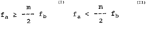
21 video signal is represented as fa, then:
-5-
PATENT
390100-2418
m
1 if fa >_ ---- fb, then ~2fa - mfb - fb~ ? 0.15fb; and
2
m
2 if fa _< --_ fb, thbn ~mfb --2fa - fb~ ? 0.15fb, where m
2
3 is an integer.
fb
4 As a feature of this invention, °- <_ 0.4.
Advantageously, the burst clock signal has a modulation figure in
6 the range from 0.7 to 1.4
Tf the processed video signal is a time division
8 multiplexed signal (wherein the luminance and chrominance
9 components of the video signal are time division multiplexed),
successive horizontal periods of the.TDM video signal are
11 separated by a horizontal blanking interval to which the burst
12 clock signal is added. In one embodiment, the burst clock signal
13 is added to the achromatic level of the TDM video signal; and in
14 another embodiment, the burst clock signal is superimposed onto
the horizontal synchronizing signal, normally included in the y
16 horizontal blamking interval.
l'7 BRIEF DESCRIPTION OF THE DRAWINGS
18 The following detailed description, given by way of
19 example, will best be understood in conjunction with the
accompanying drawings in which:
l
~'~~'~~,.
PAT~raT
' 390100-2418
1 FIG. 1 is a schematic representation of video signal
2 waveforms in which a burst clock.signal is rsacorded with a
3 processed video signal;
4 FIG. 2 is a schematic representation of preferred video
signal,waveforms wherein a burst clock signal is recorded with a
6 processed video signal;
? FIG. 3 is a block diagram of burst and synchronizing
8 signal recovery apparatus that may be used to recover the burst
9 clock signal and the horizontal synchronizing signal recorded as
shown in FIG. 2;
11 FIG. 4 is another block diagram of apparatus for
12 recovering the recorded video and burst clock signals shown in
13 FIG. 2;
14 FIG. 5 is a graphical representation of the spectrum of
a spurious signal that may be produced if a pulse-count type of
15 demodulator is used to recover the recorded video signal;
1? FIGS. 6A and 6B comprise a block diagram of one
18 embodiment for recording and reproducing video signals wherein
19 the present invention finds ready application;
2p FIGS. ?A-?E are useful in understanding the manner in
21 which the video signals are recorded by the apparatus shown in
22 ~ FIGS. 6A and 6B;
_?_
o"~(~~ J'o ~~,
PATENT
390100-2418
1 FIG. f3 is a schematic representation of a
2 record/playback head assembly used with the apparatus of FIGS. 6A
3 and 6B; and .
4 FIGS. 9A and 9B are schematic representations of eight
successive tracks in which a frame of HDTV s:Lgnals is recorded
5 together with PCM audio signals by the embodiment shown in FIGS.
? 6A and 6B.
g DETAILED DESCRIPTION OF A PREFERRED EMBODIMENT
g Referring to FIG. 2, there is illustrated a schematic
waveform representation, of the blanking interval which separates
11 two successive horizontal periods of a processed video signal.
12 In the video recording environment described herein, the
13 processed video signal is a time division multiplexed (TDM) video
14 signal and will be described in greater detail hereinbelow. As
compared to the schematic waveform representation of FIG.~1, it
16 is seen that the horizontal blanking period of FIG. 2 is
1'7 narrower; and the burst clock signal B is superimposed onto the
18 sync tip level of the negative-going horizontal synchronizing
19 signal H. Moreover, the duration of the horizontal synchronizing
signal is greater in FIG. 2 than in FIG. 1.
21 Although the horizontal blanking interval of FIG. 2 is
22 preferred, the present invention may be used with the wider
23 horizontal blanking interval shown in FIG. 1. In FIG, 1, the
_g_
PATENT
390100-248
1 burst clock signal is superimposed onto the DC level which
2 corresponds to the blanking level. In FIG. 2, the burst clock
3 signal is superimposed onto the DC level which corresponds to the
4 horizontal sync tip. Thus, .from FIGS. 1 and 2, the burst clock
signal may be superimposed on the achromatic level of the TDM
6 video signal. If the TDM video signal, horizontal blanking
7 interval and horizontal synchronizing signal are frequency
8 modulated for recording purposes, the present invention proceeds
g an the recognition of a desired relationship between the
modulating frequency fa which represents the DC level onto which
11 the burst clock signal is superimposed and the burst clock
frequency fb. Now, assuming that m_ is an integer, if
m
13 fa > --_ fb, then (2fa - mfb - fb( >_ 0.~.5fb. However, if
2
m
14 fa < _-_ fb, then (mfb -2fa - fb( >_ 0.15fb.
2
Typical examples of fa and fb may be, for instance, fa = 18.5 MHz
16 and fb = 4.995 MHz.
17 As mentioned previously, the addition of the burst
18 CIUCk signal to the horizontal blanking interval shown in FIG. 2
is preferred, although the present invention produces improved
2.0 results even if the burst clock signal is added to the horizontal
21 blanking interval of the type shown in FIG. 1. In the FIG. 2
-9-
~~~'""~d ~"
PATENT
390100°2418
1 configuration, the horizontal synchronizing signal may be
2 suffiaient~.y wide as to occupy substantially the entire duration
3 of the blanking interval. Lt is appreciated that this width
4 facilitates the recovery of the horizontal synchronizing signal
during a playback mode. Additionally, m ~m rye.
6 configuration, since the burst clock signal is superimposed onto
7 the wide horizontal synchronizing signal, a sufficient number of
8 cycles of the burst clock are provided as to facilitate the
9 extraction of the burst clock by relatively simple and
inexpensive means, such as a relatively simple bandpass filter.
12 Consequently, the configuration shown in FIG. 2 results in
12 accurate, reliable and stable separation during a playback mode
13 of the horizontal synchronizing signal and, additionally, assures
14 that the clock signal will be accurately recovered from the
reproduced burst clock signal.
1~ One embodiment adapted to recover the horizontal
17 synchronizing signal and the burst clock signal from reproduced
18 frequency modulated TDM video signals is illustrated in FIG. 3.
19 Here, an input terminal 51 is adapted to receive ~.he video signal
reproduced from, for example, a record medium, after that video
21 signal 3nas been frequency demodulated. A bandpass filter 52 and
22 a low pass filter 53 are coupled to input terminal 51; and the
23 bandpass filter passes the signal component having the burst
-10-
PATENT
390100-2418
1 clock frequency fb, while the low pass filter extracts the
2 horizontal, synchronizing singal. ,
3 Alternatively, bandpass filter 52 rnay be replaced by a
4 high pass filter. Also, low pass filter 53 may be replaced by a
trap circuit. In any event, it is appreciated that the burst
6 clock signal and the horizontal synchronizing signal may be
7 easily separated from the reproduced frequency demodulated video
8 signal. The separated burst clock signal is supplied to a phase
9 locked loop (PLL) and the synchronizing signal is supplied to a
sync separator. As a result, the horizontal synchronizing signal
11 is properly separated, and the phase locked loop responds to the
12 separated burst clock signal to generate the clock signal for
13 recovering the reproduced video signal.
14 FIG. 4 illustrates mother embodiment for recovering a
clock signal from the recorded clock burst signal, and for using
16 that clock signal to recover the video signal reproduced from the
17 record medium. An input terminal 61 is supplied with the
18 reproduced frequency demodulated video signal which, as discussed
19 above, and as shown in FIG. 2, includes the horizontal
synchronizing signal and the burst clock signal superimposed
21 thereon. A low pass filter 62 extracts the TDM component From
22 the demodulated video signal and couples the extracted TDM
23 component to an analog-to-digital (A/D) converter 63. A bandpass
-11-
~~'~~1.
PATENT
390100°2418
1 filter 64 also is coupled to input terminal 61 and functions to
2 pass the demodulated burst clock signal included in the
3 reproduced video signal. Alternatively, the raur5~ ~:1~
4 may be passed by a high pass filter.. In either event, the burst
clock signal that is extracted from the demodulated video signal
6 is supplied to a gated phase locked loop 65.
7 Another low pass filter 66, which may be similar to low
g pass filter 53 of FIG. 3, is coupled to input terminal 61 and is
adapted to extract. the horizontal synchronizing signal from the
demodulated video signal. Alternatively, a trap circuit may be
11 used to extract the horizontal synchronizing signal. This
12 extracted signal is applied to a synchronizing separator 67
13 which, in turn, produces a horizontal synchronizing signal.
14 Thus, the combination of bandpass filter 64, low pass filter 66
and synchronizing separator 67 serve to separate the burst clack
16 signal end the horizontal synchronizing signal from the
17 reproduced demodulated, video signal.
lg The separated synchronizing signal is applied to the
19 gated phase Locked loop as a gate signal. Accordingly, the gated
phase locked loop is enabled during the interval that the burst
21 clock signal is expected (as seen from FIG. 2) and regenerates
22 the clock signal therefrom. This clock signal is supplied to A/D
23 converter 63 for digitizing the TDM signal component extracted by
-12-
~~~'~~~"
PATENT
390100-2418
l low pass filter 62. The digitized TDM component then is coupled
2 from an output terminal 68 to further processing circuitry,
3 whereby the original video signal is recovered.
4 As is knawn, white noise is converted to noise
exhibiting a triangular-shaped spectrum by a frequency
6 demodulator. Accordingly; it is preferable that the relationship
7 between the burst clock frequency fb and the modulating frequency
8 fa be limited as follows:
fb
_____ < 0.4.
fa
If the frequency modulated video signal which is
11 reproduced from the record medium is demodulated by a pulse-count
~, type demodulator, a spurious signal may be produced. FIG. 5 is a
l3 graphical representation of the spectrum of this spurious signal
14 and its relationship to the burst clock frequency fb and
~ modulating frequency fa. The frequency of this spurious signal
16 may be represented as FSp, wherein Fop = 2fa - mfb. As seen in
1~ FIG. 5, as m increases, the amplitude of the spurious signal
1g decreases .
19 To extract the burst signal of frequency fb from the
spectrum illustrated. in FIG. 5, a bandpass filter having a pass
21 band fbW on the order of about 0.3fb may be used. FIG. 5
-13-
~~c~F~rG~.~.
PATENT
390100-2418
1 illustrates the pass band of this filter in broken lines, and the
2 aforementioned limitation on its bandwidth is seen to result in
3 the extraction of the burst clock signal without interference
4 from spurious signal components. A bandwidth fbw on the order of
about 0.3fb permits the implementation of a relatively efficient
6 bandpass filter at reasonable cast.
7 In the foregoing equations which represent the
8 relationship between the clock burst frequency fb and the
9 modulating frequency fa, and in the=equation which represents the
20 spurious signal F'Sp, the integer m typically may be m = 5, 6, 7
11 or 8.
12 In view of the aforementioned relationship between the .
13 burst clock frequency fb and the modulating frequency fa, the
14 amplitude of the burst signal may be increased so as to improve
its S/N ratio without introducing any significant disturbance or
16 distortion in the reproduced burst clock signal. Preferably, the
17 modulation figure of the burst clock signal is selected to be in
1g tie range of from 0.7 to 1.4. This limitation in the modulation
19 figure further improves the S/N ratio and contributes to further
reduction of burst clock signal disturbance. Furthermore, and as
21 is seen from FIG. 2, since the horizontal blanking interval may
22 be narrowed (as is readily seen by comparing FIG. 2 to FIG. 1~,
-14-
PATENT
390100--2418
1 the duration of the TDM video signal may be increased. Hence,
2 more information may be provided in the TDM signal period.
3 Although the signal configuration represented by the
4 waveform shown in FIG. 2 is preferred, the present invention may
be used with the configuration represented by the waveform of
6 FIG. 1. Tn either case, the DC level portion of the TDM video
7 signal onto which the burst clock signal is superimposed is the
8 achromatic level of the TDM signals. In FIG. 1, this DC level is
9 tha usual blanking level and in FIG. 2, this DC level is the sync
tip level of the horizontal synchronizing signal. Since the DC
11 level is the achromatic level, the dynamic range of the digital-
12 to-analog (D/A} converters used for recording and for
13 reproduction may be used most effectively.
14 Referring now to FIGS. 6A and 6B, there is illustrated
a block diagram of a video tape recorder capable of recording and
16 reproducing an HDTV signal and which may be of the general type
17 described in the aforementioned U.S. application (attorney's ,
1g docket 390100-2420} or in Japanese Laid-Open Patent Publication
19 No. 63-194494. As described therein, and as will be explained in ,
greater detail below, the chrominance signal of the input HDTV
21 signal is corlwerted into a line sequential chroma signal which is
22 timebase expanded, timebase compressed and multiplexed with the
23 HDTV luminance component to form a TDM signal which then is
-15-
PATENT
390100-2418
1 separated unto a plurality of channels for recording by a plural-
2 channel head assembly. It is assumed, for the purpose of the
3 present description, that the HDTV signal is separated into its
4 luminance component Y, supplied to an input terminal 1, and red
and blue chrominance components CR and CB supplied to input
6 terminals 4r and 4b, respectively. The luminance component Y is
7 digitized by an analog-to-digital (A/D) converter 2 at a rate
8 determined by a sampling clock signal of frequency fA. The
9 digitized luminance component is separated into two channels A
and B and written into line memories 3A and 3B, respectively, in
11 response to a write clock signal of frequency fA. As will be
12 discussed, alternate lines of the digitized luminance signal are
13 written into line memories 3A and 3B, respectively.
14 The red and blue chrominance components supplied to
input terminals 4r and 4b are in the form of red and blue color
16 difference signals R-Y and B-Y, respectively. These color
17 difference chrominance components are digitized by A/D converters
1g 5r and 5b, respectively, at a rate determined by a sampling clock
19 of frequency f$. The digitized color difference signals then are
written into line memories 6r and &b, respectively.
21 A synchronizing signal included in the HDTV signal is
22 separately supplzed to an input terminal 7 for coupling to a
23 control circuit 8. This control circuit is provided with a
-16-
F'AT~;NT
390100-2418
1 reference clock signal of frequency fx generated by a crystal
2 oscillator,9 which, as is appreciated, exhibits a very stable
3 frequency. The purpose of control circuit 8 is to generate
4 several different clock signals derived from the reference clock
frequency fX and synchronized with the HDTV synchronizing signal.
6 These different clock signals are used to sample the luminance
7 and chrominance components, to write the digitized luminance and
8 chrominance components into line memories, to read those
9 digitized components from the Line memories, to timebase compress ,
the luminance and chrominance components and to timebase compress
11 a digitized audio signal, all of which are described below.
12 The digitized luminance components stored in line
13 . memory 3A are read therefrom in response to a read clock of
14 frequency fc produced by control circuit 8. The digitized red
color difference component CR written into line memory 6r is read
16 from this line memory by the read cloak fC and is combined in a
17 summing circuit 10A with the luminance component read from line .
18 memary 3A. Similarly, the luminance component stored in line
19 memory 3B is read therefrom by the read clock fc and is combined
in summing circuit 10B with the blue color difference component
21 CB read from line memory 6b.
22 Summing circuit 10A functions to combine odd line
23 intervals of luminance component Y and odd line intervals of red
-17-
PATENT
390100-2418
1 color difference component CR to produce the combined signal TDM.
2 Similarly,, summing circuit lOB functions to combine the even line
3 intervals of luminance component Y read from :line memory 3B and
4 even line intervals of blue .color difference component CD read
from line memory 6b to produce the signal TDM. These TDM signals
6 produced by summing circuits l0A and 10B are written inta a frame
7 memory 11 in response to the read clock fC.
g The TDM signals of alternate line intervals stored in '
9 frame memory 11 are read therefrom at a rate which, in the
present embodiment, is less than the memory write rate.
11 Consequently, the frame memory functions to timebase expand the
12 TDM signals; and these timebase expanded video signals are
13 coupled to digital-to-analog converters 12A and 12B by way of
14 adding circuits 40A and 40B, respectively, which are adapted to
add to the TDM signals the burst clock signal fb generated by
16 control circuit 8, resulting in the combined signals as shown in
17 ETG. 2. As an example fb = f~/~. The D/A converters return the
1g TDM signals to analog form at a rate determined by clock fC
19 supplied to the D/A converters by the control circuit.
The combined burst clock and TDM analog signals
21 produced by D/A converters l2A and 12B are coupled to emphasizing
22 . and frequency modulating circuits 14A and 14B, respectively,
23 whereat the combined signals are converted to FM signals for
-18-
PATENT
390100-2418
1 recording. It is appreciated that adders 40A and 40B combine the
2 burst clock signal and the TDM signals with the timing
3 relationship shown preferably in FIG. 2, or as shown in FIG. 1,
4 whereby the burst clock signal is superimposed onto the DC level
of the horizontal blanking interval (as shown in FIG. 1) or,onto
F the horizontal synchronizing signal (as shown in FIG. 2).
The FM video signals from modulators 14A and 14B are
8 coupled to adders l3A and 13B, respectively (FIG. 6B}, whereat
9 they are combined with information .signals (to be described)
added thereto in multiplexed format. The resultant multiplexed
11 signals are supplied to respective recording heads 17A and 17B by
12 recording amplifiers 15A and 15B via record/playback switches 16A
13 16B, respectively, as more clearly shown in FIG. 6B. It is
14 appreciated that recording heads 17A and 17B are mounted on a
recording head drum 70 which rotates to scan successive slant
16 tracks across a magnetic tape 18 which is deployed about the head
1? drum with a wrap angle no greater than 180°
18 In the example illustrated herein, audio information
19 signals, preferably pulse code modulated (PCM) audio signals, are
multiplexed with the video and burst clock signals. As more
21 clearly shown in FIG. 6B, stereo right and left audio signals are
22 supplied to an audio signal recording and processing circuit 41
23 which operates to encode the digitized audio signals as PCM
-19-
PATENT
390100°2418
1 signals and, preferably, processes the digitized signals in
2 accordance~with conventional error correction techniques. The
3 resultant PCM audio signals.are written into a frame memory (nat
4 shown) and subsequently read therefrom at a read-out rate
determined by a read clock generated by control circuit 8. The
6 frame memory serves to timebase compress the PCM audio signals;
7 and these compressed signals are supplied~to adding circuits 13A
8 and 13B.
g A servo circuit 19 (FIG. 6B) is supplied with a
reference clock signal fn from control circuit 8 for controlling
11 the rotation of heads 17A, 17B as well as the transport speed of
12 tape 18. Accordingly, the servo circuit is adapted to control a
13 head drive motor 20 which is coupled to head drum 70 for
14 rotatably driving heads 17A and 17B. The servo circuit also is
coupled to a capstan drive motor 2l which drives a capstan 22 to
16 transport tape 18.
17 When recorded high-definition television signals are to
18 be reproduced from magnetic tape 18, the signals recorded thereon
19 are reproduced by heads 17A, 17B and supplied through record/
playback switches 16A, 16B to servo circuit 19 and also to
21 playback amplifiers 23A, 23B. The amplified FM signals are
22 coupled to de-emphasizing and frequency demodulating circuits
23 24A, 24B as well, as to an audio signal reproducing and processing
-20-
PATENT
390100-2428
1 circuit 42 which recovers the PCM audio signals and converts them
2 to analog left and right audio signals. Stereophonic audio
3 signals, for example, reproduced by the audio reproducing and
4 processing circuit are applied to output terminals 43L, 43R.
De-emphasized and frequency-modulated signals from de
emphasizing and frequency demodulating circu~.ts 24A, 24B are
7 supplied to clock generators 27A, 27B, which may be of the type
8 shown in FIGS. 3 or 4, to recover the clock signal from the
9 reproduced burst clock signal. The recovered clock signal is
supplied to A/D converters 25A, 25B and also to timebase
11 correctors 26A, 26B for correcting timebase fluctuations 'that may
. 12 be present in the reproduced signals.
13 ' Corrected TDM signals from the timebase correctors 26A,
14 26B are written into a frame memory 28 from which the._signals are
read and supplied to line memories 30A, 30B as well as to line
16 memories 34r and 34b. Luminance signals are read from line
17' memories 30A, 30B and are added by an adder 31, whose sum signal .
lg is then supplied through a D/A converter 32 to an output terminal
19 33f thereby recovering the luminance signal Y. Chrominance
signals are read from line memories 34r and 34b and supplied to
21 interpolating circuits 35r, 35b which produce interpolated
22 , representations of those line intervals of chrominance signals
23 that were not recorded. Thus, successive lines of chrominance
-21-
~'~c~~~~.,
PATBNT
390100-2918
1 signals are coupled through D/A converters 36r, 36b to output
2 terminals 37r, 37b whereat the chroma signals CR, CB are
3 recovered.
In operatian, the'luminance component Y supplied to A/D
converter 2 is sampled to produce digitized representations of
6 successive line intervals as shown in FIG. 7A. In one
7 embodiment, 1320 samples are generated during each line interval
8 and, in accordance with this example, the horizontal blanking
9 interval is comprised of about 200 samples.
Similarly, the red color difference component CR
11 supplied to A/D converter 5r is digitized to produce digital
12 representations of successive line intervals of the red color
13 difference signal, as shown in FIG. 7B. The luminance component
14 sampling clock frequency fA is approximately four times the
chrominance sampling clock frequency fB, whereupon the
16 chrominance component is sampled at a rate sufficient to produce
17 about 330 samples during each line interval. Of these, the
18 horizontal blanking interval is comprised of approximately 50
19 samples.
In a similar manner, the blue color difference
21 component CB supplied to A/D converter 5b is digitized in
22 response to the chrominance sampling clock frequency f~ to
-22-
.
PATENT
390100-2418
1 produce digital representations of successive line intervals, as
2 shown in FIG. ?C.
3 In one embodiment, the reference clock frequency fx ,
4 produced from crystal oscillator 9 is a fraction of the
fundamental clock frequency of the HDTV signal, the latter being
6 equal to 74.25 MHz. In this embodiment,
7 fx = fp~ _ X3/5) x ?4.25 = 44.55 MHz = 1320 fHz
8 wherein fHZ = 33.75 KHz and is the horizontal line frequency of
9 the HDTV signal.
As mentioned above, fB = fA/4 = 33o fHl.
11 In accordance with the foregoing, and as shown in FIGS.
12 ?A-?C, the luminance component is represented by 1320 samples per
13 dine interval, the red color difference component CR is
14 represented by 330 samples per line interval and the blue color
7.5 difference component CB likewise is represented by 330 samples
16 per line interval. The luminance component samples are written
17 into line memories 3A and 3B; and the chrominance component
18 samples are written into line memories Or and 6b, respectively.
19 In particular, each line memory has written thereinto alternate
line intervals. Thus, the luminance component line intervals
21 written into line memory 3A may be represented as Y1, Y3, Y5,
22 etc.; the luminance component line intervals written into line
23 memory 3B may be represented as Y2, Y4, Y6, etc.; the line
=23-
PATENT
390100-2418
1 intervals of the red color difference component written into line
2 memory 6r may be represented as CR1, CR3, CRS, etc. and the line
3 intervals of the blue color difference component written into
4 line memory 6b may be represented as CB2, CB4, CB6, etc.
The alternate line intervals stored in the respective
6 line memories are read therefrom at the read-out rate fc whi.ch,
7 in the preferred embodiment, is about one-half the luminance
8 write clock rate fA. As a result, the luminance component read
9 from line memories 3A and 3B is timebase expanded while the
chrominance components read from line memories 6r and 6b are
11 timebase compressed. The luminance component read from line
12 memory 3A is combined with the chrominance component read from
13 line memory 6r in summing circuit 10A, resulting in the TDM
14 signal schematically illustrated in FIG. 7D. Similarly, the
luminance component read from line memory 3B is combined with the
16 chrominance component read from line memory 6b in summing circuit
17 lOB to produce the TDM signal schematically illustrated'in FIG.
28 7E. As a result, the combined samples read from line memories 3A
19 and 6r occupy a duration corresponding to two HDTV line
intervals, as shown in FIG. 7D; and, simis.arly, the combined
21 samples read from line memories 3B and 6b occupy two HDTV line
22 intervals, as shown in FIG. 7E. Notwithstanding this conversion
23 of the time axis, substantially all of the luminance and
-24-
PATENT
390100-2418 .
1 chraminance component samples that had been written into the
2 respective. line memories are read therefrom. For convenience,
3 the combined timebase converted video signal produced by summing
4 circuit 10A is identified as the channel A timebase converted
video signal and the combined timebase converted video signal
6 produced by summing circuit 10B is referred to as the channel B
~ timebase converted video signal.
8 Tf the number of horizontal~line intervals included in
9 an HDTV frame is represented as L, the number of samples
generated during each line interval is represented as S and the
11 read cloak rate fC is half the luminance component write clock
12 rate fA, then the relationship between L, S and fC may be
13 expressed as:
L x S
14 __________ _ constant
2f~
Zf L = 1125, S = 1320 and fc = 44.55/2 MHz, then:
L x S 1125 x 1320
lfi ______ __ _ _____________
2fC ~ 44.55 x 10⁶
1~ From the foregoing relationship, it is appreciated that if the
18 number of line intervals included in an ~iDTV frame increases and
19 if the number of samples produced during each line interval also
increases, then the read clock rate fC will increase. For
21 example, if L = 1332 and S = 1500, then:
-25-
a
PATENT
390100-2418
1332 x 1500 37
1 fc = _____________ _ 29.97 MHz = 880 fH~ _ ____ fA
2 55
2 In one numerical example th~.burst clock signal frequency
3 fb = f~/6 = 4.995 MHz.
4 In the example discussed above, the channel A timebase
converted video signal supplied to frame memory 11 by summing
6 circuit lOA is comprised of odd line intervals of the luminance
7 component Y and the red color difference component CR, as shown
8 in FIG. 7D. Similarly, the timebase converted video signal
9 supplied to the frame memory by summing circuit lOB is comprised
of the even line in't~rvals of the luminance component Y and the
11 blue color difference component CB, as shown in FIG. 7E. If the
12 read clock rate fc is greater than fA/2, it is seen that 'the
13 duration of each effective horizontal period of the time base
14 converted video signal supplied to frame memory 11 is less than
twice the HDTV line interval. However, for convenience, it is
16 assumed hereimthat fc = fAi2 and, therefore, the duration of
17 each of the channel A and channel B horizontal periods (shown in
18 FIGS. 7D and 7E~) is equal to twice the HDTV horizontal interval.
19 The channel A and channel B timebase converted video signals are
written into frame memory 11 at 'the fC rate.
21 After being written into the frame memory, the timebase
22 converted video signals are read therefrom at the fC rate and
-26-
~~~~~x.
PAT~:NT
390100-2418
1 combined with the burst clock signal as mentioned above.
2 Preferably, the channel A timebase converted video signals are
3 supplied, by way of D/A converter 12A, emphasizing and FM circuit
4 14A, adding circuit 13A and .recording amplifier 15A to head 17A.
Similarly, the channel B timebase converted video signals which
6 are read from frame.memory ll are supplied to head 17B for
7 recording. As heads 17A and 17B scan successive tracks across
8 magnetic tape 18, the odd timebase converted line intervals shown
9 in FIG. 7D are recorded in each track traced by head 17A and the
even timebase converted line intervals are recorded in each track
11 traced by head 17B. As will be described, heads 17A and 17B are
12 included in two diametrically opposed head assemblies, with one
13 such assembly being comprised of heads 17A1 and 17B1 and the
14 other assembly being comprised of heads 17A2 and 1?B2. The pair
of heads included in each assembly are angularly displaced from
16 each other in the scanning direction, as will also be described.
17 Consequently, heads 17A1 and 17B1 simultaneously record adjacent
lg tracks wherein the track recorded by head 17A1 is formed of odd
line intervals and the track recorded by head 17B1 is formed of
even line intervals; and when heads 17A2 and 17B2 simultaneously
21 scan magnetic tape 18, head 17A2 records a track of odd line
22 intervals and head 17B2 records a track of even line intervals.
-27-
PATENT
390100-2418
1 In the embodiment wherein the read clock rate fC is
2 slightly greater than one-half the write clock rate f~, the
3 duration, or horizontal period, of a timebase converted line
4 interval read from frame memory 11 is less than twice the HDTV
line interval. Thus, the timebase converted video signal in, for
6 example, channel A does not completely "fill" the converted (or
7 doubled) HDTV line interval. Therefore, all of the timebase
8 converged video signals read from frame memory 11 when, for
9 example, head.l7A~ traces a track maybe recorded in a length
that is less than the.angular extent that this head is in contact
11 with the tape. Stated otherwise, the timebase converted video
12 signal recorded in each track occupies a length that is less than
I3 the 180° angular extent that the head contacts the tape. This
14 extra, or blank space in the track is occupied by the PCM audio
15' signal produced by audio signal recording and processing circuit
16 41.
It is preferred that heads 17A1 and 17B1 are included
18 in one head assembly and heads 1?A2 and 17B2 are included in
19 another head assembly., FIG. 8 schematically illustrates a
typical head assembly 71 comprised of a pair of heads 71a and 71b
~1 which are displaced, or offset from each other in the track
22 scanning direction and are additionally displaced from each other
23 by an amount h in a direction parallel to the axis of rotation.
-28-
PATENT
390100-2418
1 It is appreciated that this displacement h defines the track
2 pitch g. FIG. 8 also schematically illustrates different azimuth
3 angles formed in heads 7la end 7lb which, as is known to those of
4 ordinary skill in the art, minimizes crosstalk interference due
to the pinking up of signals from an adjacent track that had been
6 recorded with a head having a different azimuth. Head assembly
71 is effective to record two slant tracks simultaneously by
8 heads 71a and 71b, respectively, as this head assembly rotates to
9 scan a trace across tape 18. It will be seen that one complete
rotation of the rotary drum results in the tracing of four
12 successive tracks, two by one head assembly and two by the other
12 head assembly. In the preferred embodiment, one frame of the
13 HDTV signal is recorded in eight tracks and, therefore, two
14 complete rotations of head drum 70 are effective to record one
frame of the HDTV signal. Stated otherwise, the heads are
16 rotated at twice the HDTV frame rate.
17 FIGS. 9A and 9B illustrate one embodiment of the track
1g pattern recorded by. two rotations of 'the two head assemblies to
19 record one frame of the HDTV signal together with the PCM audio
signal. It will be appreciated that, during the first half of
21 the first rotation of the head drum, tracks A and B of segment 1
22 are recorded by heads 17A1 and 17B1, respectively. Although not
23 shown in FIGS. 6A and 6B, it should be understood that the
_29-
~~~~ c'~s~~.,
PATEhIT
3901.00-2418
1 multiplexed video and PCM audio signals supplied to the trailing
2 head is delayed by an amount sufficient to align or match the
3 starting ends of tracks A and B. During the second half of the
4 first rotation, heads 17A2 and 17B2 record tracks A and B of
segment 2. In similar fashion, during the first half of the
6 second rotation, heads 17A1 and 17B1 record tracks A and B in
7 segment 3; and during the second half of this second rotation,
8 heads 17A2 and 1782 record tracks A and B of segment 4.
9 Accordingly, one frame of the HDTV signal is recorded in four
segments, each segment being formed of two tracks in which two
11 channels are recorded, respectively. It is seen that the PCM
12 audio signal is recorded ahead of the timebase converted video
13 signal in the blank portion produced as a result of the timebase
14 compression of the video signal.
As shown in FIGS. 9A and 9B, each track is sufficient
16 to record 166.5 horizontal periods. Included in these 166.5
17 horizontal periods are the PCM audio signal, the timebase
18 converted video signal arid several periods in which other
19 information may be recorded. More particularly, the 166.5
horizontal periods correspond to a tape wrap angle of 180°, of
21 which 23.66° is allocated for the recording of audio information.
22 The beginning portion of a track, corresponding to about l.2°,
23 comprises a margin area during which the recording head moves
-30-
PATENT
390100-2418
1 into contact with the tape sufficient to record the PCM audio
2 signal.
3 A preamble area corresponding to 2.0° follows the
4 margin area; and two channels of PCM audio signals are recorded
thereafter in a length corresponding to 8.0°. A post-amble area
6 of 1.2° follows the PCM audio signal section, and this, in turn,
7 is followed by a guard band area corresponding to 1.2°. The
8 preamble, PCM audio signal and post-amble areas comprise a first
9 audio signal recording section. Then, a second audio signal
recording section is recorded, comprised of a preamble area of
11 2.0°, a PCM audio signal area of 8.0° and a post-amble area
of
12 1.26°. A guard band area of length corresponding to 2 horizontal
13 periods separates the audio signal recording area from the video
~.4 signal recording area. As an example, a ~~1m411 ~l ~ .~~~s~.~~~~~.~
periods. (2H) corresponds to about 2.16°.
16 The beginning portion of the video signal recording
17 area contains information signals such as vertical synchronizing
18 signals Vl and V2, automatic gain control (AGC) signals, clamping
19 signals, and the like. These signals are recorded in a section
of the track which precedes the timebase converted video signal
21 information and has a length of; for example, 11 or 11.5
22 horizontal periods. For example, this section of the video
23 signal recording area is comprised of 11 horizontal periods'(11H)
-31-
~~~~~a~~.
PATENZ'
390100-2418
1 when odd segments (e.g. segments 1 and 3) are recorded and has a
2 length of 11.5H when even segments (e.g. segments 2 and 4) are
3 recorded. This is illustrated more particularly in FIG. 9B.
The timebase converted video signals then are recorded
in the video signal recording area following the recording of
6 these information signals. As illustrated in FIG. 9A, 129
7 horizontal periods (129H) of timebase converted video signals are
8 recorded in the video signal recording area. Each.track then
9 concludes with a margin area of length corresponding to 1H or
1.5H. If the aforementioned information signals are recorded in
11 an area corresponding to 11H, such as in the odd segments, 'then
12 this concluding margin area is of a length equal to 1.5H.
13 However, if the information signals are recorded in a length
14 corresponding to 11.5H, as in the even segments, then this margin
area is recorded with a length of 1H.
16 It will be recognized that, in a given track, only red
17 color difference chrominance components or only blue color
18 difference chrominance components are multiplexed with the
19 luminance component for recording. For example, in each track A,
the luminance component is multiplexed with the blue color
21 difference component. However, i.n each trac)c B, the luminance
22 ~ component is multiplexed with the red color difference component.
23 ~'he respective original HDTV line intervals from which the
-32-
PATENT
390100-?.418
1 multiplexed luminance and chrominance components are derived also
2 are indicated in FIG. 9A.
3 It is seen that 143.5 horizontal periods, corresponding
4 to a length of 155.14°, are ,recorded from the beginning of the
first guard band area to the end of a track. This length is
comprised of the following signals:
Guard Band Area 2. OH
g Information Signal Area 11.0H
Video Signals 129. OH
Margin Area 1.5H
11 Total Length 143.5Hi
12 In FIG. 9B, two PCM audio signal sections are provided
13 in the audio signal recording area. This permits the recording
14 of audio information from two audio systems, each comprised of
two channels. For example, left and right stereo audio signals
16 may be recorded in one PCM audio signal recording section and two
channels of SAP audio signals may be recorded in the other PCM
18 audio signal recording section. Of course, the present
19 explanation is not limited to the particular channels, audio
systems or audio information that is recorded in the audio signal
21 recording area. Nevertheless, it is seen that the PCM audio
22 signals recorded ire one section may be independent of the PCM
23 audio signals recorded in the other.
-33-
PATENT
390100-2418
While the present invention has been particularly shown
2 and described with reference to a preferred embodiment, it will
3 be readily appreciated by those of ordinary skill in the art that
4 various changes and modifications may be made without departing
from the spirit and scope of the invention. For example, each
6 head assembly has been described as including two heads far
7 recording two tracks simultaneously. If desired, three or more
8 heads may be provided in each head assembly. Furthermore, the
present invention is not limited solely to the recording of HDTV
and audio signals. If desired, a standard video signal may be
11 recorded in accordance with this invention. Additionally, other
12 information may be time division multiplexed with the video
13 signals for recording, and the present invention is not limited
14 solely to the use of PCM audio signal information.
Therefore, it is intended that the appended claims be
16 interpreted as including the embodiment described herein,
17 alternatives which have been discussed above and all equivalents
18 thereto.
-34-