Language selection

Search

Patent 2050119 Summary

Third-party information liability

Some of the information on this Web page has been provided by external sources. The Government of Canada is not responsible for the accuracy, reliability or currency of the information supplied by external sources. Users wishing to rely upon this information should consult directly with the source of the information. Content provided by external sources is not subject to official languages, privacy and accessibility requirements.

Claims and Abstract availability

Any discrepancies in the text and image of the Claims and Abstract are due to differing posting times. Text of the Claims and Abstract are posted:

  • At the time the application is open to public inspection;
  • At the time of issue of the patent (grant).
(12) Patent: (11) CA 2050119
(54) English Title: CIRCUIT FOR RECORDING AND REPRODUCING TIME BASE ERROR CORRECTOR REFERENCE SIGNAL
(54) French Title: CIRCUIT D'ENREGISTREMENT ET DE LECTURE DE SIGNAUX DE REFERENCE POUR CORRECTEUR D'ERREURS DE BASE DE TEMPS
Status: Expired and beyond the Period of Reversal
Bibliographic Data
(51) International Patent Classification (IPC):
  • H04N 05/95 (2006.01)
  • H04N 09/82 (2006.01)
  • H04N 09/89 (2006.01)
(72) Inventors :
  • KO, JEONG-WAN (Republic of Korea)
(73) Owners :
  • SAMSUNG ELECTRONICS CO., LTD.
(71) Applicants :
  • SAMSUNG ELECTRONICS CO., LTD. (Republic of Korea)
(74) Agent: SMART & BIGGAR LP
(74) Associate agent:
(45) Issued: 1997-12-16
(22) Filed Date: 1991-08-28
(41) Open to Public Inspection: 1992-05-20
Examination requested: 1991-08-28
Availability of licence: N/A
Dedicated to the Public: N/A
(25) Language of filing: English

Patent Cooperation Treaty (PCT): No

(30) Application Priority Data:
Application No. Country/Territory Date
90-18736 (Republic of Korea) 1990-11-19

Abstracts

English Abstract


A circuit for recording and reproducing a TBC reference
signal for use in video recording/reproducing systems
includes a circuit for adding to a video signal to be
recorded a TBC reference signal in which the TBC reference
signal has a period adaptively varying corresponding to a
synchronizing variation of the video signal; and a circuit
for extracting and reproducing a TBC reference signal from a
video signal read-out from the recording medium in order to
correct time base errors in the video signal. The circuit
corrects time base errors of the video signal according to a
TBC reference signal reproduced along with the video signal
from the recording medium during reproduction.


French Abstract

Circuit permettant d'enregistrer et de reproduire un signal de référence de correcteur d'erreurs de temps (TBC) pour l'utiliser dans des systèmes d'enregistrement/reproduction vidéo. Comprend un circuit pour combiner à un signal vidéo à enregistrer un signal de référence de TBC ayant une période adaptable correspondant à une variation de synchronisation du signal vidéo; et un circuit pour extraire et reproduire un signal de référence de TBC à partir d'un signal vidéo lu sur un support d'enregistrement afin de corriger les erreurs de temps du signal vidéo. Le circuit corrige les erreurs de temps du signal vidéo conformément à un signal de référence de TBC reproduit conjointement avec le signal vidéo lu sur le support d'enregistrement pendant la reproduction.

Claims

Note: Claims are shown in the official language in which they were submitted.


THE EMBODIMENTS OF THE INVENTION IN WHICH AN EXCLUSIVE
PROPERTY OR PRIVILEGE IS CLAIMED ARE DEFINED AS FOLLOWS:
1. A circuit for generating a time base correction
reference signal, the circuit being included in a video
recording/reproducing system including a recorder for
recording a video signal on a recording medium and a
reproducer for reproducing the video signal recorded on the
recording medium and correcting time base error, the
circuit comprising:
means included in said recorder for generating
said time base correction reference signal at least during
each blanking period of a video signal that is to be
recorded at least at times other than its blanking periods;
means included in said recorder for recording at
least at times other than its said blanking periods said
video signal to be recorded;
means included in said recorder for selectively
recording said time base correction reference signal during
and only during said blanking periods;
means included in said reproducer for reproducing
said selectively recorded time base correction reference
signal and said recorded video signal from said recording
medium;
means for separating said selectively recorded
time base correction reference signal from said recorded
video signal reproduced from said recording medium; and
means for correcting time base errors of said
video signal reproduced by said reproducer in response to
said time base correction reference signal separated
therefrom.
2. A circuit for recording/reproducing a time base
correction reference signal as claimed in claim 1, wherein
said time base correction reference signal is added during
and only during said blanking periods to said video signal
to be recorded.
19

3. A circuit for recording/reproducing a time base
correction reference signal as claimed in claim 2, wherein
during and only during said blanking periods said time base
correction reference signal is substituted for a video
signal originally supplied for recording, in said video
signal as actually recorded.
4. A circuit for recording a time base correction
reference signal, said circuit comprising:
means for modulating a carrier with a video signal
having blanking intervals therewithin in which
synchronizing signals are included;
means for generating a time base correction
reference signal at least during each said blanking period
of said video signal, said time base correction;
means for adding said time base correction
reference signal to a modulated video signal from said
video signal modulating means by alternatively providing
one of said time base correction reference signal and said
modulated video signal;
means for recording said modulated video signal to
which said time base correction reference signal is added
by said reference signal adding means, on the recording
medium;
means included in said recorder for generating
said time base correction reference signal at least during
each blanking period of a video signal to be recorded at
least at times other than its blanking periods;
means included in said recorder for recording said
video signal at least at times other than its said blanking
periods to be recorded; and
means included in said recorder for selectively
recording said time base correction reference signal during
and only during said blanking periods.
5. A circuit for recording a time base correction
reference signal as claimed in claim 4, wherein said

reference signal adding means comprises a mixer for mixing
said modulated video signal and said time base correction
reference signal.
6. A circuit for recording a time base correction
reference signal as claimed in claim 5, wherein said
reference signal adding means further comprises adding time
control means for enabling said time base correction
reference signal to be added during a blanking interval of
said modulated video signal.
7. A circuit for recording a time base correction
reference signal as claimed in claim 6, wherein said time
base correction reference signal is distributed in a
frequency bandwidth sufficiently larger than that of other
signals in a blanking interval of said modulated video
signal but smaller than that of the high frequency cut-off
of said modulated video signal.
8. A circuit for recording a time base correction
reference signal as claimed in claim 6, wherein said
reference signal adding means further comprises standard
modulated signal generating means for generating modulated
signals for use as a standard in a blanking interval in
order that the modulated signals can be inserted into the
blanking interval of the modulated video signal together
with said time base correction reference signal to prevent
external disturbances.
9. A circuit for recording a time base correction
reference signal as claimed in claim 8, wherein said time
base correction reference signal is distributed within a
frequency bandwidth which is sufficiently larger than that
of said standard modulated signal for use in a blanking
interval but smaller than that of the high cut-off
frequency of said modulated video signal.
21

10. Apparatus for recovering a video signal used to
frequency modulate a carrier wave recorded on a recording
medium together with a time base correction reference
signal of a frequency corresponding to the frequency of
said frequency-modulated carrier wave when modulated with
a sustained value of said video signal, all the respective
portions of which time base correction reference signal
occur during and only during blanking intervals of said
video signal, said circuit comprising:
means for reproducing from said recording medium
a reproduced signal comprising said frequency modulated
carrier wave accompanied by said time base correction
signal, respective portions of which said time base
correction signal occur during and only during blanking
intervals of said video signal;
means for demodulating said reproduced signal,
sensitive to said frequency-modulated carrier wave but not
to said time base correction signal, to generate a
demodulated video signal that is unaccompanied by said time
base correction signal;
a time base correction circuit for correcting time
base errors of said demodulated video signal in response to
a continuously supplied time base correction reference
signal applied thereto;
means for separating a time base correction
reference signal from said reproduced signal by selecting
portions said reproduced signal that are in the frequency
range of said time base correction reference signal and
that occur during and only during blanking intervals of
said demodulated video signal, thereby to generate a
separated time base correction reference signal having
respective segments which occur during and only during
blanking intervals of said demodulated video signal; and
means, responsive to said segments of said
separated time base correction reference signal, for
generating said continuously supplied time base correction
reference signal applied to said time base correction
circuit.
22

11. Apparatus as claimed in claim 10, wherein said
means for separating a time base correction reference
signal from said reproduced signal comprises a band-pass
filter for selecting portions of said reproduced signal
that are in the frequency range of said time base
correction reference signal.
12. A video recording device for generating video
signals having time base correction reference signals for
recordation, said device comprising:
means for generating modulated video signals by
modulating received video signals; means for separating
horizontal synchronization signals from said received video
signals;
means for generating time base correction
reference signals having periods varying in response to
period variations of said horizontal synchronization
signals; and
means for combining said time base correction
reference signals into horizontal blanking intervals of
said modulated video signals and providing resultant
signals to a recording element.
13. A video recording device as claimed in claim 12,
wherein said combining means comprises:
means for generating gating pulses during
horizontal blanking intervals of said received video
signals; and
switching means for alternatively providing said
modulated video signals during horizontal scanning
intervals and said time base correction reference signals
during said horizontal blanking intervals in response to
said gating pulses.
14. A video recording device as claimed in claim 12,
further comprising:
23

means for generating modulated blanking pulses by
detecting and frequency modulating blanking pulses of said
horizontal synchronization signals; and
said combining means combining said modulated
blanking pulses into said horizontal blanking intervals of
said modulated video signals.
15. A video recording device as claimed in claim 12,
wherein said gating pulses are generated by delaying said
synchronizing pulses.
16. A video recording device as claimed in claim 12,
further comprising:
means for generating modulated blanking pulses by
detecting and frequency modulating blanking pulses of said
horizontal synchronization signals;
means for generating modulated synchronizing
pulses by detecting and frequency modulating synchronizing
pulses of said horizontal synchronization signals; and
wherein said combining means comprises means for generating
combined signals by adding said modulated blanking pulses,
said modulated synchronizing pulses, and said time base
correction reference signals,
means for generating gating pulses during
horizontal blanking intervals of said received video
signals; and
switching means for alternatively providing said
modulated video signals during horizontal scanning
intervals and said combined signals during said horizontal
blanking intervals in response to said gating pulses.
17. A video recording device for generating video
signals for recordation, said device comprising: means for
generating modulated luminance signals by modulating
separated luminance signals; means for separating
horizontal synchronization signals from said separated
luminance signals; means for generating time base
24

correction reference signals; and means for alternatively
providing said modulated luminance signals during
horizontal scanning intervals of said modulated luminance
signals and said time base correction reference signals
during horizontal blanking intervals of said modulated
luminance signals to a recording element.
18. A video recording device as claimed in claim 17,
further comprised of said reference signal generating means
generating said time base correction reference signals
having periods varying in response to period variations of
said horizontal synchronization signals.
19. A video recording device as claimed in claim 17,
further comprising: means for generating modulated blanking
pulses by detecting and frequency modulating blanking
pulses of said horizontal synchronization signals; means
for generating modulated synchronizing pulses by detecting
and frequency modulating synchronizing pulses of said
horizontal synchronization signals; and wherein said
alternatively providing means comprises:
means for generating combined signals by adding
said modulated blanking pulses, said modulated
synchronizing pulses, and said time base correction
reference signals;
means for generating gating pulses during
horizontal blanking intervals of said separated luminance
signals; and
switching means for alternatively providing said
modulated luminance signals during horizontal scanning
intervals and said combined signals during said horizontal
blanking intervals in response to said gating pulses.
20. A video recording device as claimed in claim 18,
further comprising:
means for generating modulated blanking pulses by
detecting and frequency modulating blanking pulses of said
horizontal synchronization signals;

means for generating modulated synchronizing
pulses by detecting and frequency modulating synchronizing
pulses of said horizontal synchronization signals; and
wherein said alternatively providing means comprises:
means for generating combined signals by adding
said modulated blanking pulses, said modulated
synchronizing pulses, and said time base correction
reference signals;
means for generating gating pulses during
horizontal blanking intervals of said separated luminance
signals; and
switching means for alternatively providing said
modulated luminance signals during horizontal scanning
intervals and said combined signals during said horizontal
blanking intervals in response to said gating pulses.
21. A video recording device as claimed in claim 18,
further comprising: means for generating modulated blanking
pulses by detecting and frequency modulating blanking
pulses of said horizontal synchronization signals; and said
alternatively providing means combining said modulated
blanking pulses into said horizontal blanking intervals of
said modulated luminance signals.
22. A video recording device for generating video
signals for recordation, said device comprising:
luminance/chrominance separating means for
generating separated luminance signals and separated
chrominance signals from received composite video signals;
means for generating modulated luminance signals
by modulating said separated luminance signals;
means for generating modulated chrominance signals
by modulating said separate chrominance signals;
means for separating horizontal synchronization
signals from said separated luminance signals;
means for generating time base correction
reference signals having periods varying in response to
26

period variations of said horizontal synchronization
signals; and
switching means for generating combined signals by
alternatively providing said modulated luminance signals
during horizontal scanning intervals of said modulated
luminance signals and said time base correction reference
signals during horizontal blanking intervals of said
modulated luminance signals; and
means for generating recording signals by mixing
said combined signals and said modulated chrominance
signals; and
head means for recording said recording signals on
a recording medium.
23. A video recording device as claimed in claim 22,
further comprising: means for generating modulated
blanking pulses by detecting and frequency modulating
blanking pulses of said horizontal synchronization signals.
24. A video recording as claimed in claim 22, further
comprising means for generating replacement modulated
blanking pulses and replacement modulated synchronizing
pulses and adding said replacement modulated blanking
pulses and said replacement modulated synchronizing pulses
to said horizontal blanking intervals of said modulated
luminance signals as substitutions for original signals of
said horizontal blanking intervals.
25. A video recording device as claimed in claim 22,
further comprising: means for generating modulated
blanking pulses by detecting and frequency modulating
blanking pulses of said horizontal synchronization signals;
means for generating modulated synchronizing pulses by
detecting and frequency modulating synchronizing pulses of
said horizontal synchronization signals; and wherein said
switching means comprises:
27

means for generating added signals by adding said
modulated blanking pulses, said modulated synchronizing
pulses, and said time base correction reference signals;
means for generating gating pulses during
horizontal blanking intervals of said modulated luminance
signals; and
switching means for alternatively providing said
modulated luminance signals during horizontal scanning
intervals and said added signals during said horizontal
blanking intervals in response to said gating pulses to
generate said combined signals.
26. A video reproducing device for regenerating video
signals from a record medium, said device comprising: means
for separating modulated video signals from video
information regenerated from said record medium; means for
generating demodulated video signals by demodulating said
modulated video signals; time base correction control means
for generating control signals in response to gating pulses
and in response to time base correction reference signals
contained in said modulated video signals; video signal
time base correction means for generating time base
corrected video signals by time base correcting said
demodulated video signals in response to said control
signals; means for separating horizontal synchronization
signals from said time base corrected video signals; and
means for generating said gating pulses during blanking
intervals of said demodulated video signals responsive to
the separated horizontal synchronization signals.
27. A video reproducing device as claimed in claim 26,
wherein said time base correction control means is a burst
injection locked oscillator circuit receiving said time
base correction reference signals only when said gating
pulses are indicative of said blanking intervals of said
horizontal synchronization signals to regulate a frequency
of said control signals in response to said time base
corrected reference signals.
28

28. A video reproducing device as claimed in claim 26,
wherein a frequency of said control signals is regulated in
response to said time base corrected reference signals.
29. A video reproducing device as claimed in claim 26,
wherein said time base correction reference signals are
contained only in blanking intervals of said modulated
video signals.
30. A video reproducing device for regenerating video
signals from a record medium, said device comprising:
luminance/chrominance separating means for
separating modulated luminance signals and modulated
chrominance signals from video information regenerated from
said record medium;
means for generating demodulated luminance signals
by demodulating said modulated luminance signals; means for
generating demodulated chrominance signals by demodulating
said modulated chrominance signals;
burst injection locked oscillator means for
receiving time base correction reference signals contained
in said demodulated luminance signals in response to gating
pulses and regulating a frequency of output signals
therefrom in response to the received time base correction
reference signals;
luminance time base correction means for
generating time base corrected luminance signals by time
base correcting said demodulated luminance signals in
response to said output signals;
chrominance time base correction means for
generating time base corrected chrominance signals by time
base correcting said demodulated chrominance signals in
response to said output signals;
means for separating horizontal synchronization
signals;
means for generating said gating pulses during
blanking intervals, the positions in time of which blanking
29

intervals are calculated in response to said separated
horizontal synchronization signals; and
means for generating composite video signals by
combining said time base corrected luminance signals and
said time base corrected chrominance signals.
31. A video reproducing device as claimed in claim 30,
further comprised of said burst injection locked oscillator
means receiving said time base correction reference signals
only in blanking intervals of said modulated luminance
signals.

Description

Note: Descriptions are shown in the official language in which they were submitted.


CIRCUIT FOR RECORDING AND REPRODUCING
TINE BASE ERROR CORRECTOR REFERENCE SIGNAL
Background of the Invention
The present invention relates to a time base error
corIector (TBC) for correcting timing discordance of video
signals in video signal recording/reproducing systems, and
more particularly to a circuit for Iecording and reproducing
a reference signal used for correcting timing discordance of
video signals.
Generally, a video signal includes video information
arranged in accordance with a synchronizing signal so as to
display accurate images on display devices, and is affected
by noise during recording and reproducing through a
recording medium as are any other information signals,
thereby producing time base er-rors in the video information.
Time base errors occur mainly due to mechanical elements
included in the recording/reproducing apparatus, which can
tire viewers due to trembling of an image caused by the
temporal lengthening or shortening of the signal.
Especially when an analogue video signal is converted
to a digital video signal for digitally processing the
analogue video signal, a variation in the sampling number
may occur due to the time base error though the number of
~,

2 ~
sampling for each synchronization is required to be
constant As a result, video information designated for each
pixel may move to the left or to the right by several
pixels, so that the phase of the signal is not fixed and
furthermore, signal processing between frames becomes
impossible due to the changing pixel positions.
A time base error corIector (hereinafter referred to as
a TsC) is an apparatus that corrects the timing discordance
of video information due to time base error of the video
signal, and which is employed to remove the time base errors
created during recording and reproducing and to
resynchronize the signal more precisely in video Iecording
and reproducing systems.
A conventional TBC used in video recording and
reproducing systems will be described below, refeIring to
FIG.1 of the accompanying diagrammatic drawings.
In FIG.1, analog to digital converter (A/D converter)
lo samples by a certain period and encodes a video signal
entering through input line 5, thereby generating a digital
video signal. Memory 20 temporarily stores the digital video
signal converted in the A/D converter lo. Digital to anaiog
converter (D/A converter) 30 converts the digital video
signal read-out from the memory 20 to an analog video signal
and outputs it through output line 15. To maintain uniformly
the set number of samplings of A/D converter 10 and the
number of data stored in memory 20 for every horizontal
, .... . .. .. ... ..

synchIonization, storing clock geneIatoI 40 generates
stoIing clocks having diffeIent peIiods accoIding to the
period variation of a horizontal synchronizing signal of a
video signal supplied through input line 5 and supplies the
storing clocks to A/D converter 10 and memory 20. Reading
clock generator 50 generates a reading clock having a
certain peIiod and supplies the clock to memory 20 and D/A
converter 30. In the storing clock generator 40 for
generating stoIing clocks, synchronizing signal separator 41
sepaIates a horizontal synchIonizing signal fIom a video
signal supplied through input line 5 and phase comparatoI 42
compares the phase of the frequency-divided storing clock
applied from frequency divider g4 with that of the
horizontal synchronizing signal supplied from the
synchronizing signal separator 41 and generates a control
voltage corresponding to the phase difference. Voltage
controlled oscillatoI 43 ( hereinafteI referred to as VCO
generates storing clocks having different frequencies
depending on the control voltages applied from the phase
comparator 42 and supplies the clocks to A/D converter 10,
memory 20 and frequency divider 44. The frequency divider 44
frequency-divides the storing clocks in order that the
clocks have the same frequency as that of the horizontal
synchronizing signal and supplies the clocks to phase
comparator 42.
~ ~ , , .; .
- . . ~ , ; .
:,
, . . ~ ~.. . ..
. .

~3~
Finally, the conventional TBC shown in FIG.1 samples a
video signal by a certain number of samplings for each
horizontal synchIonizing period by regulating
(adding/subtracting) the fIequency of storing clock
according to the period va~iation of the horizontal
synchronizing signal and stores the video signal into the
memory. Then, such video data stored in the memory is read-
out by the reading clock of the certain frequency and is
converted to an analog video signal to correct the timing
discordance of the video information of the video signals.
However, in the case of the circuit shown in FIG.1, a
negative feedback circuit is provided between the phase
comparator 42 and the VCO in order to regulate
(add/subtract) the frequency of the storing clock for every
horizontal synch~onizing signal period. The time constant of
the negative feedback circuit usually has a time period
which is at least greater than the horizontal synchronizing
signal period and usually of two or thIee times the
horizontal synchronizing signal period. When the fIequency
transfeI chaIacteristic of a recording system is very narrow
as compared with the band of an original signal, rise time
and fall time of the horizontal synchronizing signal
lengthens to make it dif~icult to locate a precise
synchIonizing position. FurtheImore, due to the influence of
noise and the like, the frequency of the storing clock
cannot be changed precisely according to the variation of
, . ~ . . .................. . .
- - ~- : ~
,, . - , . . .
. : ~ , ;.................. ~

the horizontal synchronizing signal period. FOT these
reasons, time base correction of a video signal can not be
caIried out precisely.
Summary of the Invention :
Therefore, it is an object of the present invention to
provide a CiICUit for recording and reproducing a Tsc
reference signal, in a video recording/reproducing system,
which records a TBC reference signal with a video signal on
a recording medium, and then corrects the time base errors
of the video signal by the reproduced TBC reference signal
so that pIecise time base error correction is attained.
To attain the above object, a circuit for recording a
TBC reference signal of the present invention comprises
means for modulating a video signal so as to be recorded on
a recording medium, means for generating a TBC reference
signal having a period varying according to a synchronizing
state of the video signal, means for adding the TBC
reference signal to a modulated video signal from the video
signal modulating means, and means foI recording the
modulated video signal to which a TBC Ieference signal is
added by the reference signal adding means, on the recording
medium.
To attain the above object, a circuit for reproducing a
TBC reference signal of the present invention comprises
. , . . ~ -~ . , , : -
. . ~ . . . ~ , . ...................................... ..
'. . '. ' '' '~ '

A~
means for reading out video information in which a TsC
reference signal is inserted, from a recording medium, means
for demodulating the read-out video information to generate
a video signal, a TBC circuit for correcting time base
errors of the demodulated video signal by the TBC reference
signal, means for separating a Tsc reference signal from the
read-out video signal, and means for restoring the extracted
TBC reference signal to supply the restored TBC reference
signal to the TBC circuit.
Brief Description of the Drawings
These and other advantages of the present invention
will be more apparent by describing preferred embodiments of
the present inventi.on with reference to the attached
drawings, in which:
FIG.1 iS a block diagram of a conventional time base
corrector;
FIG . 2 iS a bloc.k diagram of one example of a circuit
for recording a reference signal for correcting time base
error, according to one embodiment of the pIesent invention;
FIGs.3A and 3B illustrate the frequency characteIistics
:of a video signal processed by the circuit shown in FIG . 2;
and
~ FIG.4 is a block circuit diagram of an embodiment of
~ the circuit for reproducing a reference signal for
, 6

2~
correcting time base error according to the present
lnvent lon .
Detailed Description of the Invention
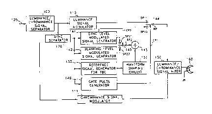
ReferIing to FIG.2 wherein an embodiment of a circuit
for recording a reference signal for correcting a time base
eIror according to the pIesent invention is shown, input
line 105 is connected to an external video signal source
(not shown) and to the input terminal of
luminance/chrominance signal separator 100. A first output
terminal of the luminance/chrominance signal separator 100
is connected to the input terminals of synchronizing signal
separator 120 and luminance signal modulator 110. A second
output terminal of the luminance/chrominance signal
separator 100 is connected to an inp-ut terminal of
chrominance signal modulator 111. An output terminal of the
luminance signal modulator 110 is connected to a first
selection point SP11 of a first controlling switch 144. The
reference connection point RP1 of the first contIolling
switch 144 is connected to a first input terminal of
luminance/chrominance signal mixer lS0. The output terminal
of chrominance signal modulator 111 is connected to a second
input terminal of luminance/chrominance signal mixer 150. An
output terminal of luminance/chrominance signal mixer 150 is
connected to magnetic head 160. An output terminal of

~5~ 9
synchronizing signal separator 120 is connected to input
terminals of TBC reference signal generator 130,
synchronizing level modulated signal generator 141, blanking
level modulated signal generator 142 and gate pulse
generator 146. An output terminal of TBC reference signal
geneIator 130 is connected to an input terminal of waveform
shaping circuit 131. An output terminal of the waveform
shaping circuit 131 is connected to a first input terminal
of referenc-e signal mixer 143~ A first output terminal of
synchronizing level modulated signal generator 141 is
connected to a first selection point SP21 of a second
controlling sw-itch 145. A second output terminal of
synchronizing level modulated signal generator 14-1 is
connected to c-ontrol port CP2 of the second controlling
switch 145. An ~utput terminal of blanking level modulated
signal generator 142 is connected to a second selection
point SP22 of the second controlling switch 145. An output
terminal of the s.econd controlling switch 145 is cQnnected
to a second input terminal of reference signal mixer 143.
The output teIminal of the reference signal mixe~ 143 is
connected to a second selection point SP12 of the first
controlling switch 144. An output terminal of gate pulse
generator 146 is connected to control port CPl of the first
controlling switch 14-4.
FIGs.3A and 3B show characteristics of the output
. .. :; , .,, . ~ : ,., . :
.
:,, ~ : : :
.,. ~ ,
. . .

2~
frequency of the luminance /chrominance mixer 150 in the
circuit shown in FIG.2, wherein FIG.3A is for frequency
characteristics of the video signal in a horizontal scanning
period and FIG.3B is for frequency characteristics of the
video signal in a horizontal blanking interval.
In FIG.2, luminance/ chrominance signal separatoI 100
separates video signals input through the input line 105
into a luminance signal and a chrominance signal and
supplies the luminance signal to the input terminals of
luminance signal modulator 110 and synchronizing signal
separator 120 th~ough the fi.rst output terminal and supplies
the chrominance signal to the input terminal of chrominance
signal modulator 111 through the second output terminal.
In luminance signal modulatoI 110, the frequency of the
l.uminance signal is frequency-modulated by a carrier s.ignal
s-o as to be recorded on a recording medium and the modulated
luminance signal distributed in the same manner as the
luminance signal of FIG.3A is ~upplied to the first
selection point SPll of the first controlling switch 14~.
.
In chrominance signal modulator 111, the amplitude o-f a
chrominance signal is modulated to be distributed in the
~ frequency ba~d of from 0 to 1.2MHz in the same manner as the
'; chrominance signal of FIG.3A and the low frequency converted
chrominance signal is supplied to the second input terminal
of luminance/chrominance signal mixer 150.
Synchronizing signal separator 120 separates a
,'
~ . .. . . . . . . .

\J ~ .'3
horizontal synchronizing signal fIom the luminance signal to
supply to the input terminals of the synchronizing level
modulated signal generator 141, the blanking le~el modulated
signal generato~ 142, the TBC reference signal generator 130
and the gate pulse generatoI 146.
Referen-ce signal gene~ator 130 consists of a voltage
controlled oscillator 43, a phase comparatoI 42 and a
frequency divider 44 of a st-oIing clock generator 40 as
shown in FIG.l, detects the pel-iod variat-ion of the
horizontal synchronizing s,ignal input from the sy~chronizing
signal separator 120, and generates a TBC Ieference signal
in the form of a clock pulse having a period varying in
response to the period vari-ation of the detected horizontal
synchro~izing signal.
Waveform shaping circuit 131 filters the TBC reference
signal in clock pulse form and -generates,a TBC reference '~
signal waveformed to a sine wave.
Synchronizing level modulated signal generator 141
detects a synchronizing pulse from the horizontal
synchronizing signa}s, applies a logic signal of a certain
logic state ( high or low logic state) to the control port
CP2 of the second cont~ol,ling switch 145 during detection of
the synchronizing puls-e, and supplies a synchronizing level
modulated signal which is generated by frequency~modulating
the detected synchronizing pulse by a carrier signal, to the
,. , . ~ :.

2 ~
first selection point SP21 of the second controlling switch
145. The synchronizing level modulated signal generator 141
can be composed of a level detector, an oscillator and a
mixeI to operate as described above, which aIe not shown in
the drawing.
Blanking le~el modulated signal generator 142 detects a
blanking pulse from the horizontal synchronizing signals and
supplies the blankin-g level modulated signal which is
gener-ated by frequency-modul.ating the detected blanking
pulse level by a carrier s-i-gnal, to the seco-nd selection
point SP22 of the sec~nd controlling switch 145. In ordeI
foI the opeIation to ta-ke place, t-he blanking level
modulated signal generator 142 can be composed of a level
detector, an oscillator and a mixer.
The second contr~Lling switch 145 operates when a logic
signal is applied to the contrQl port CP2 from the second
output terminal of the synchronizing level modulated signal
generator 141, and selects the output of the synchronizing
~:~ level modulated s-ignal generator 141 connected to the first
selec.tion point SP21 and supplies the result to the second
input terminal of the reference signal mixer 143 during the
synchronizing pulse duration of the horizontal synchronizing
signal. On the other hand, the second controlling switch 145
selects the output of the blanking level modulated signal
generator 142 connected to the second selection point SP22
~ and supplies the result to the second input terminal of the
11
.,
r- - : ..................... .
.. .. ' ' . ~'

3 L~
reference signal mixer 143 during the intervals other than
the synchronizing pulse period duration of the horizontal
synchronizing signal.
The reference signal mixeI 143 mixes the waveform-
shaped TBC Ieference signal supp.lied from the waveform
shaping CiICUit 131 with the modulated signals supplied
f~om the reference connection point RP-2 of the second
co~.tIo:llin-g switch 145 and supplies the mixed signals to the
secon.d selection connection point SP12 of the first
contr-oIling switch 144.
The fIequencies of the signals aIe divided in the
wavefo:~m shapi.ng circuit 131 and are waveformed to a sine
wavefoIm in oIder that the sync-h~onizing level modulated
signal is dist-ri-buted around the zone of 3.4MHz, the
blanki-ng- level modulated signal is distributed aIound the
zon-e of 3.68MHz, and the TBC ref~rence signal is distributed
aroun~ the zone o-f 5MHz as shown in FIG.3B-. The reason why
the TB-C Ieference signal is supplied to the first
con.tr:o:lling switch 144 after being mixed with the blanking
level modulated signal and synchronizing level modulated
signal, is to prevent the appearance of the effects of
higher harmonics and reflected waves on the output video
signal by the noise included in the blanking interval and
synchIonizing period of the modulated luminance signal in
which the TBC refeIence signal is to be inserted and by the
... ., - . . . .............. .. - . . ~ . - . . .
~ , : : . . : .
.. ..
- . .. ~ - ; . . ~ ~ . . .

insertion of the reference signal.
In order to determine a region among the luminance
signals in which the TBC refeIence signal is to be inserted,
gate pulse generator 146 detects a synchIonizing pulse or
blanking pulse from the horizon.tal synchronizing signals,
delays t.he detected synchron;~ing pulse or blanking pulse by
a certain period ( for instance, 55~) shorter than the
period of the horizontal synchronizing signal, generates a
gate pulse having a width sufficient to cove:I the blank:ing
interval of the horizontal sy-n-chroniz-ing s-ignal ~y th-e
delayed pulse and supplie-s the gate pulse to the control
port CP-1 of the f-rst controlling switch 144.
The fir-st controllin.~ s-witch 144 selects the output of
the reference sig~al mixer 14.3 supplied to the second
selection point SP12 while th:e gate pulse is applied fr~m
the gate pulse generator 146 to the control port CP1 and
supplie-s the result to the fiIst input terminal of the
luminance/chrominance signal mixer 150. On the otheI hand,
during the time that the ga-te pulse is not applied to the
con-trol port CP1, the first controlling switch ls4 selects
the output of the luminance signal modulator 110 supplied to
the first selection point SP11 and supplies the selected
output to the luminance/chrominance signal mixer 150.
Luminance/chrominance signal mixer 150 mixes the
modulated luminance signal, in which the TBC refeIence
signal is inserted, supplied from the reference connection
~,, . -. - : ; , : :
. ~ . . . . . . .
. .
.
:'

pOillt RP1 of the first controlling switch 144 with the low
frequency converted chrominance signal supplied from the
chrominance signal modulator 111 and record~ the mixed
signals on a recording medium through magnetic he~d 160. The
video signal mixed in the lumi-nance/chrominance mixer 150
has such frequency charact.eristics as show-n in FIG . 3A duri~g
a hoIi.zontal scAnning period., and has such frequency
characteristic.s as shown in FIG . 3B during a blanki.ng
interval.
When the sync~r-onizing signals of the video signal are
changed by the e-ffect o-f a time bas:e error, the TBC
reference signal re.cor-ded with the video signal is chan.ged
by the same amount o-f change as that oc~urring in the
synchroni.z-i-ng signals. Accordi~gly, the video information of
the video signal is time base corrected duling repro-ducing
by the changed TBC r-eferen.c*-si-gn-al, thereby performi~g the
coIrection pr-ecisely.
FIG.4 is a blQck diag~am of an embodiment of a circui.t
for reproducing a T~C reference signal according to the
present invention. In F'IG.4, magnetic head 300 i9 connected
to the input terminal of luminance/chIominance signal
separator 310. A first input terminal of t.he
luminance/chrominance signal separator 310 is connected to
input terminals of luminance signal demodulator 320 and band
pass filter 351 and a second input terminal of the separato
14
. ,, . .. . -- - . , ;: .- ., ,. - -.
- : ~ , ,.
- . : , . : .
;

2 ~
310 is connected to an input terminal of chrominance signal
demodulatoI 321. An output terminal of the luminance signal
demodulator 320 is connected to an input terminal of a first
TBC circuit 330. An output terminal of the fiISt TBC circuit
330 is conne.cted to an input teIminal o-f synchronizing
signal s~eparator 361 and to a first input terminal of
composite video signal geneIator 340. An output terminal o-f
the band pass filter 351 is connected to an input terminal
o:-f burst injection locking circuit 360 ( hereinaft~r
refelred to a.s BILC ). An outpu-t terminaI of BILC 360 is
connect.ed to contr~l terminals of the first TBC circuit 330
a-nd a second TBC circuit 331. An outpu-t termin~l of
synchronizing signal separator 361 is connected to an inp~t
terminal of gate pulse geneIatoI 362. The gate pulse
generatoI 362 is conne.ct-ed to a control terminal of BILC
360. An output termi-nal of chrominance sig-nal demodulatoI
321 is connecte~ to an input terminal of the second TBC
circuit 331. An output terminal of the seco-nd TBC circuit
331 is connected to a second input terminal of cQmposite
video sign-al geneIatoI 340.
An output line terminal 305 of the composite video
signal gene~a-toI 340 is connected to an external display
device or other vide.o recording systems (not shown).
In opeIatioDi, magnetic head 300 reads out video
information from a recording medium and supplies the
information to luminance/chrominance signal sepaIator 310
. , ,

2 ~
Luminance/chrominance signal sepaIator 310 separates
the video infoImation supplied from the magnetic head 300
into a luminance signal mixed with a TBC reference signal
and a ch~ominance signal.
T,l]r~nAnce signal demod~ to~ 3,20 fIequency-demo-dulat-.~s
the luminanc,e slgnal mixed with the TBC refeIenc-e signal a-nd
supplies the demodulate-d l--m;n~nce signal to the first Tsc
ci~cuit 330.
Band pass filter 351 de-t-ec~ the T~C reference sign~l
by band-pass filte-ring the luminance signal mixed with th-e
TBC reference sig-n,a'l.
When a gate pulse is applied to the control terminals,
BILC 3-60 receiv-es th~ TBC rRference sig~al detected in the
ba~d pass filter 351 and r-e-gulates an output frequency
according to the fIequ-ency of th-e inp~t TBC I-eferen-ce
signal. ~hen, the BILC 3-60 ge-nerates a clock pulse-6h-aped
TBC reference signal having a regulated output frequency and
supplies the generated sign~l to the control terminals of
the first and second TBC CiICUitS 330 and 331.
The first TBC circuit 330 corrects the time base error
of the demodulated lumina~ce signal input from the luminance
signal demodulatQr 320 'Qy the TBC reference signal input
from the BILC 360 and generates the corrected luminance
signal. Synchron;~i~g signal separator 361 separates a
horizontal synchronizing signal from the corrected luminance
16
', , t '

signal and supplies the synchronizing signal to gate pulse
generator 362.
Gate pulse gen-erator 362, which include.s a del.ay device
and a monost:able multi~vibrator therein, dela-ys a
synchroniz:ing pulse of a horizontal s-ynchro.nizin-g signal
u~,til the nex.t sync-hronizing pul.se OCCUIS by the delay
d~vice an:d g~ler.dt~., in t.he mQnostable mult,i-vibrator, a
gate pulse havi~g a.widt-h.suf,ficient to cover the blanking
int-e-rval of t-ke hQ-r~iz.ontal synchIonizing signal by the
synchronizing pul~e of the delayed hoIizo~ta:l synchronizing
signal. The gate pulse is supplied to the co.ntrol terminal
of the BILC 360 to control the regulation of the QUtp,Ut
frequency of t~e B.ILC 360 during the b-laDking int-elv-al of .,,
the horiz-ontal synchr-onizing signal. .
Chrominance sign-al demodulator 321 gener,:at-es the
demodulate~d chromin~ce si-gnal by anp-litude-demodulating the
extrac-t-ed chr-omi-~a~ce :signal.
: ~The second T~C circuit 331 coIrects the time base error
: o:f t.he dem~dul~.ted chromina-nce signal by the TBC r-eference
sign-al, to gene-rate the corrected chr,ominance signal.
Composite video signal generator 340 mixes the
correc:ted luminance signal and the cQrr.ected chrominance
s,ignal to gene~:ate a composite video signal and supplies it
to a disp,lay.appara-tus or other image Iecording systems
through the output line 305.
The embodiments of the present invention that are
.
,~; .. ,

2 ~
described in detail above are advantageous in that, in
systems for recording and reproducing a video signal, timing
discoIdance of a video signal by a tlme base e~ror during
recordi-ng and re-producing operation~s can be adaptively
corr-ecte.d as the var..ia.tio-n of synchIonizing s-ignals of a
vide-o signal occu~ by the T~C reference signal recolded
together with the video signal.
' 18
.,
- . - .
~. - .. . .. .. ..

Representative Drawing
A single figure which represents the drawing illustrating the invention.
Administrative Status

2024-08-01:As part of the Next Generation Patents (NGP) transition, the Canadian Patents Database (CPD) now contains a more detailed Event History, which replicates the Event Log of our new back-office solution.

Please note that "Inactive:" events refers to events no longer in use in our new back-office solution.

For a clearer understanding of the status of the application/patent presented on this page, the site Disclaimer , as well as the definitions for Patent , Event History , Maintenance Fee  and Payment History  should be consulted.

Event History

Description Date
Time Limit for Reversal Expired 2010-08-30
Letter Sent 2009-08-28
Inactive: IPC from MCD 2006-03-11
Grant by Issuance 1997-12-16
Inactive: Status info is complete as of Log entry date 1997-10-08
Inactive: Application prosecuted on TS as of Log entry date 1997-10-08
Pre-grant 1997-08-15
Notice of Allowance is Issued 1997-03-18
Application Published (Open to Public Inspection) 1992-05-20
All Requirements for Examination Determined Compliant 1991-08-28
Request for Examination Requirements Determined Compliant 1991-08-28

Abandonment History

There is no abandonment history.

Maintenance Fee

The last payment was received on 1997-07-10

Note : If the full payment has not been received on or before the date indicated, a further fee may be required which may be one of the following

  • the reinstatement fee;
  • the late payment fee; or
  • additional fee to reverse deemed expiry.

Patent fees are adjusted on the 1st of January every year. The amounts above are the current amounts if received by December 31 of the current year.
Please refer to the CIPO Patent Fees web page to see all current fee amounts.

Fee History

Fee Type Anniversary Year Due Date Paid Date
MF (application, 6th anniv.) - standard 06 1997-08-28 1997-07-10
Final fee - standard 1997-08-15
MF (patent, 7th anniv.) - standard 1998-08-28 1998-06-10
MF (patent, 8th anniv.) - standard 1999-08-30 1999-07-16
MF (patent, 9th anniv.) - standard 2000-08-28 2000-07-18
MF (patent, 10th anniv.) - standard 2001-08-28 2001-07-20
MF (patent, 11th anniv.) - standard 2002-08-28 2002-07-18
MF (patent, 12th anniv.) - standard 2003-08-28 2003-07-17
MF (patent, 13th anniv.) - standard 2004-08-30 2004-07-19
MF (patent, 14th anniv.) - standard 2005-08-29 2005-07-06
MF (patent, 15th anniv.) - standard 2006-08-28 2006-07-05
MF (patent, 16th anniv.) - standard 2007-08-28 2007-07-06
MF (patent, 17th anniv.) - standard 2008-08-28 2008-07-10
Owners on Record

Note: Records showing the ownership history in alphabetical order.

Current Owners on Record
SAMSUNG ELECTRONICS CO., LTD.
Past Owners on Record
JEONG-WAN KO
Past Owners that do not appear in the "Owners on Record" listing will appear in other documentation within the application.
Documents

To view selected files, please enter reCAPTCHA code :


To view images, click a link in the Document Description column. To download the documents, select one or more checkboxes in the first column and then click the "Download Selected in PDF format (Zip Archive)" or the "Download Selected as Single PDF" button.

List of published and non-published patent-specific documents on the CPD .

If you have any difficulty accessing content, you can call the Client Service Centre at 1-866-997-1936 or send them an e-mail at CIPO Client Service Centre.


Document
Description 
Date
(yyyy-mm-dd) 
Number of pages   Size of Image (KB) 
Claims 1997-03-17 12 524
Description 1994-02-25 18 654
Claims 1994-02-25 4 130
Abstract 1994-02-25 1 22
Drawings 1994-02-25 4 81
Claims 1998-08-20 12 524
Representative drawing 1997-12-11 1 11
Maintenance Fee Notice 2009-10-12 1 170
Fees 1998-06-09 1 41
Fees 2001-01-23 1 38
Fees 1997-07-09 1 31
Fees 1996-06-04 1 29
Fees 1995-07-20 1 38
Fees 1994-08-23 1 37
Fees 1993-06-22 1 30
Examiner Requisition 1996-07-22 2 69
Prosecution correspondence 1997-01-22 4 162
PCT Correspondence 1997-08-14 1 44
Courtesy - Office Letter 1992-03-17 1 38