Note: Descriptions are shown in the official language in which they were submitted.
DOCKET NO. 17595 PATEN'r
-- 1 --
LOW POWER SWITC~ING POWER æUPPLY CIRCUITS AND M~THODS
Field o~ the Invention
This invention relatas generally to power supplies
for electronic circuitry. More spacifically, this invention
5 relates to power supply circuits having regulated voltage
outputs.
Backqround of the Invention
Process control is a long-established art which
plays a major role in managing industrial plants and
10 processes. In this art, process transmitters have been used
to monitor process variables. Having evolved from the
earliest measurement devices such as barometers and
thermometers, the process transmitter has traditionally
received a great deal of technological attention to improve
15 performance due to the need for accurate process measurement.
Since the accuracy of every measurement made in a process
control loop is directly dependent upon the accuracy of the
particular process transmitter or instrument which closes the
loop, the process transmitter plays a particularly sensitive
20 role in industrial process control systems.
Beginning in the 1950s, electrical and electronic
process control loops were a natural development from prior
- 2 - 2~5~99
electromechanical control systems. The general problem of
electronic process control is to convert a physical variable
to an electrical signal, and to subsequently transmit that
signal to a recorder and/or other control equipment which may
5 be located some distance away from the physical variable.
Early types of process control loops to accomplish this goal
were "four-wire~ systems, and were configured such that
operating power was supplied through two of the four wires and
a process signal was transmitted through the other two wires.
10 The four-wire system requires the use of amplifiers or other
signal conditioning equipment at the point of measurement in
order to supply an accurate signal representative of the
physical variable since the process signal is generally very
low. See, e.~., U.S. Patent No. 3,680,384, of Grindheim.
15 Prior four-wire transmitter systems thus required separate
power supply lines, and voltage power supplies.
After the four-wire transmitter was developed, it
became apparent that the advantages of using the same two
wires for power supply and information transmission would
20 greatly improve the process control art. The "two-wire"
transmitter was then developed and operates today in a control
loop in conjunction with an external power supply, a pair of
wires from the supply, and a transmitter connected serially
between the wires. As used herein, the term "two-wire" is
25 construed broadly to mean two conductors. Thus, the term
"two-wire" includes actual wires, twisted pairs, coaxial
cables, and other pairs of conductors.
During operation of such a two-wire transmitter
loop, the transmitter energizes a sensor element and receives
30 informational signals from the sensor element. The
information is transmitted on the pair of wires by varying the
current in the current loop. Thus the transmitter acts as a
variable current sink, and the amount of current which it
sinks is representative of the information from the sensor.
35 Such prior two-wire transmitter loops have generally been
analog in nature, and the industry standard which has
developed for two-wire transmitters is a 4 to 20 milliamp
~0~ g
-- 3 --
loop, with a variable loop supply voltage having a maximum
output of 42 volts DC. With such a low voltage supply, two-
wire transmitter loops are particularly suited for use in
hazardous environments. See, e.g., U.S. Patent No. 4,242,665,
5 of Mate.
More advanced prior two-wire transmitter control
loops exhibit high-level data communication between two-wire
transmitters and various receiving elements, for example
controllers and communication devices. The concept of digital
10 communication in 4 to 20 milliamp control systems is known for
use in the more complicated 4 to ~0 milliamp loops having both
digital and analog components. Transmitters suitable for such
purposes are usually called "smart" transmitters because they
are more accurate and have operating parameters which may be
15 remotely controlled.
The trend in two-wire transmitter loops both in the
smart, microprocessor-based transmitter area and the
traditional analog transmitter area, has been to reduce the
power requirements for components which are used in the loop.
20 This need has arisen since the amount of power which a two-
wire transmitter may draw from a current loop to use for its
operation is severely limited. With a nominal 10-volt supply,
at the bottom end of operation only about 40 milliwatts is
available to power any instrumentation in the loop. Thus with
25 large power demands on the loop, two-wire control systems may
be limited to a few low power industrial control applications.
This aspect of industrial controls competes with the general
desire to design instrumentation into the loop to simplify
loop operation and installation, and to provide intrinsic
30 safety in a low power process control environment.
This long-felt need has not adequately been met by
process control loops which have the aforementioned inherent
power budget problems. Since only 40 milliwatts of power are
available to run the circuitry in the transmitter and the
35 loop, power supply circuits have been developed which attempt
to minimize power loss in the circuit and provide steady power
levels to the control loop. Traditional methods of supplying
low power to electronic circuitry include the well known
"flyback regulator control" power supply circuits wherein the
pulse width of the output current is based on a flyback
voltage developed across an inductor in the circuit. In this
5 type of power supply circuit, a pass transistor is usually
turned on and the inductor current is allowed to rise until a
threshold is reached turning off the pass transistor.
In flyback regulator control circuits, generally two
methods have been used to sense the inductor current. The
10 flyback inductor saturation current may be sensed, or a shunt
resistor can be placed in series with the flyback inductor to
directly sense the state of the flyback inductor current.
However, both of these current sensing techniques introduce a
large amount of power loss to the power supply, and therefore
15 are unacceptable for use in low power 40 milliwatt systems.
Prior power supplies using these methods of sensing the
inductor current simply do not fulfill a long-felt need in the
art for low power loss switching power supplies for electronic
circuitry.
Two-wire transmitters are often remotely located.
The length of the wires cor.necting components in the loop can
exceed 5000 feet, and the longer wires have higher resistance.
This resistance reduces the voltage to the transmitter. Other
devices such as indicators, recorders and barriers are usually
25 added to the loop, further increasing the loop resistance.
Large amounts of loop resistance cause a wide variation in the
input voltage. Changes of load current can vary widely also
as different digital systems are accessed. The combination of
high line variation and high load variation place a difficult
30 burden on the traditional methods of switching power supply
control circuits which have the further requirement of low
startup current.
It is thus important in designing low power
electronic systems, and particularly two-wire transmitters for
35 use in process control loops, to provide switching power
supplies having low loss regulated voltage control. These
power supplies should provide a steady output to run the
ZO~ 39
- 5
electronic circuitry in the system, and should provide
reliable output voltages which are dependable for use in
sensitive electronic instrumentation. Furthermore, these
power supplies should have high efficiencies so that the power
5 output is continuously available to the system. These goals
have not previously been achieved in the switching power
supply art.
Summary of the Invention
Switching power supplies provided in accordance with
10 the present invention solve the aforementioned long-felt needs
and achieve the goals stated above. In a preferred
embodiment, a switching power supply circuit comprises linear
regulator means input with an unregulated voltage for
regulating input power to the power supply and producing a
15 linearly regulated voltage. Flyback regulator means
interfaced with the linear regulator means for controlling an
output voltage according to the unregulated input voltage is
provided. Monitoring means interfaced between the linear
regulator means and the flyback regulator means for monitoring
20 the output voltage output from the flyback regulator means and
emulating the input unregulated voltage to cause the flyback
regulator means to produce a power pulse having a pulse width
is further preferably provided.
Further in accordance with the present invention, a
25 method of providing a regulated output supply voltage is
provided. The method preferably comprises the steps of
regulating initially an input voltage to an input voltage
level, energizing an output voltage in response to the input
voltage level, sensing indirectly a current related to the
30 output voltage level to provide pulse width modulation, and
feeding back a signal indicative of the output voltage to
control a repetition rate of the output pulses.
Feedback and override control that resets an
indirect current sensing means and provides current limiting
35 for startup and short circuit protection are also
advantageously provided in accordance with the invention.
205(:~9~9
-- 6
Power supply circuits and methods provided in accordance with
the present invention provide highly efficient power supplies
with very little power loss due to regulation or control of
the circuits. To achieve these goals and objects, three modes
5 of control are preferably used. These are an indirect sense
feedforward, feedback, and an override control. Furthermore,
these circuits provide highly efficient regulated power
sources for low power electronic instrumentation, and greatly
increase the efficiency of two-wire transmitters and process
10 control loops which utilize these circuits.
Switching power supply circuits described herein
have performance efficiencies of about 90%. Such results have
not heretofore been achieved in the art and solve a long-felt
need in the art for low power loss, high efficiency switching
15 power supplies for use in low power electronic circuits and
systems.
Brief Descri~tion of the Drawin~s
Figure 1 is a block diagram of a two-wire control
system having a two-wire transmitter utilizing a switching
20 power supply in accordance with the present invention.
Figure 2 is a functional block diagram of a
switching power supply provided in accordance with the present
invention.
Figure 3 is a detailed circuit schematic of a
25 preferred embodiment of a low power loss, regulated switching
power supply provided in accordance with the present
invention.
- Detailed Description of Prsferred Embodiments
Referring now to the drawings wherein like reference
30 numerals refer to like elements, Figure 1 is a schematic block
diagram of a two-wire transmitter process control loop
utilizing a switching power supply provided in accordance with
the present invention. A two-wire transmitter lo provides an
output 4 to 20 milliamp analog signal 20 to the control loop.
35 Transmitter ~0 is preferably a two-wire transmitter which has
a sensing element 30 interfaced with a process 40 which the
loop monitors and controls. The process 40 may be any type of
industrial process such as fluid flow, level, pressure,
temperature, or any other type of process having a process
variable which it is desired to monitor. The two-wire
5 transmitter 10 may also provide control functions to the loop
and the 4 to 20 milliamp analog signal 20 may also therefore
be a 4 to 20 milliamp control signal adapted to interface with
a final control element 50.
The final control element 50 in preferred
10 embodiments comprises an analog circuit 60 directly interfaced
with the 4 to 20 milliamp analog signal 20. An analog circuit
60 is interfaced with an actuator 70 which is further
interfaced at 80 with the process 40. Analog circuit 60
receives and interprets to 4 to 20 milliamp analog control
15 signal 20 and busses this signal to the actuator 70. The
actuator 70 may actuate a valve to control the process
variable when the process is a fluid flow process, for
example. However, it will be recognized by those with skill
in the art that since other types of processes as mentioned
20 above can be monitored and controlled with the control loop
shown in Figure 1, the actuator can be modified to fit the
particular process variable which is under control in the
system. The actuator and control element 50 interfaced at 80
with the process 40 provides control of the process variable
25 in accordance with a particular control protocol that is
designed for the industrial application in which the control
system is placed.
The control system is preferably powered by a DC
power supply 90 having a fixed output of up to 42 volts DC.
30 The entire DC power to run the loop is provided by DC power
supply 90, and so the entire 4 to 20 milliamp analog range
appears on the control loop by virtue of the DC power supply
90 .
DC power supply 90 is directly interfaced to the
35 transmitter 10 to provide unregulated power to the
transmitter. Preferably, a switching power supply 100 in
accordance with the present invention regulates the power
- 8 - 2 ~ 9g
received by DC power supply go and outputs the regulated power
onto a power bus 110 to supply the various circuit components
in the transmitter lo. The circuit components in the
transmitter lo such as a digital-to-analog (D/A) converter
5 120, a system CPU 130, and the sensor 30, as well as other
necessary circuitry in the transmitter 10 and components in
the loop, have regulated power supplied to them by the
switching power supply 100. The switching power supply 100 is
preferably a 40 milliwatt power supply having an efficiency of
10 between about 30% and 90~.
In a further preferred embodiment, a digital
communications interface 140 is interfaced with the control
loop at 150 and provides the ability for the control loop to
have a digital, bidirectional communications protocol
15 superimposed on the 4 to 20 milliamp analog signal.
Communications interface 140 also busses information at 160 to
a control room or user in digital form. This digital
information is usually related to loop parameter values and
the process variable especially when the transmitter 10
20 operates in a controller mode to control the process 40.
An AC power supply 170 is optionally provided to
supply additional power to the final control element 50
especially when the actuator 70 is interfaced with an
electromechanical valve requiring a strong electromagnetic
25 force to actuate the valve. AC power 170 in preferred
embodiments provides enough power to actuate a heavv duty
control valve in pressure and flow applications.
Referring to Figure 2, a functional block diagram of
switching power supply 100 for producing an output voltage
30 (V~,) in response to an unregulated input voltage (V~), is
shown. Linear regulator means 180 provides initial regulation
of V~ (a 10 to 42 volt DC level) and initially conditions V~
to a linearly regulated voltage 190 which is further input to
the switching power supply. The linear regulator means 180
35 produces a linearly regulated voltage V~ which is used by the
rest of the circuit to produce V~,. The unregulated input
voltage V,~ is input to a monitoring means 200 which is
Z t)~ 99
preferably adapted to monitor the output voltage v~t and to
control v~, with internal timing, direct, and indirect sensing
elements which comprise the monitoring means 200.
The output 210 from the monitoring means 200 in a
5 preferred embodiment is input to standard flyback regulator
and switch means 220 which is adapted to provide an output
current 230 to an output network 240. An override feedback
block 280 preferably directly senses abnormal currents in the
flyback means 220 and resets monitoring means 200. The output
10 network 240 conditions the current and converts it to the
output voltage V~, which is then usable by the electronic
circuitry in the two-wire transmitter and powers the
instrumentation in the control loop.
In a further preferred embodiment, a feedback
15 network 250 is provided interfaced with the output network 240
for feeding back part the output voltage v~, to the monitoring
block 200 having the indirect sensing and timing elemènts
therein. In this fashion, feedback network 250 controls the
pulse repetition rate of the output.
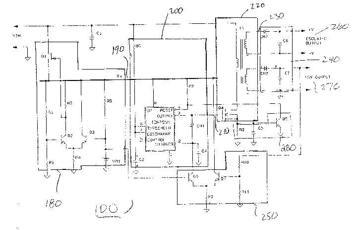
Figure 3 is a detailed circuit diagram of a
preferred embodiment of a switching power supply provided in
accordance with the present invention. In this circuit, Q1,
Q2, Q3, R1 through R5 ànd the zener diode VRl comprise the
linear regulator 180. The linear regulator 180 allows a wide
25 range of input voltages to be used, anywhere from 10 to 42
volts DC. Q2 and ~3 make up a difference amplifier circuit
wherein the difference in reference voltage and the feedback
output is amplified and drives the field effect transistor
(FET) Q1 providing series regulation of V+.
The monitoring means 200 having an indirect sensing
means and timing element comprises the components R6, R7, C2,
C4, U2 (which in preferred embodiments is an ICM7555 timing
chip hereinafter referred to as a "555 timer") and CR1. The
output from the timing chip is input at 210 to the flyback
35 regulator 220 which further comprises Q4, an insulated gate
FET or MOSFET, and an inductor coil T1 operating in the
flyback mode.
2~
-- 10 --
The current 230 output from the flyback regulator
circuit 220 is input to the output network 230 which comprises
in a preferred embodiment capacitors C6 and C7 and diodes CR2
and CR3. In a further preferred embodiment, an isolated
5 output 260 and a 5-volt output 270 are output from the output
circuit 240. In still further preferred embodiments, a
feedback signal from the s-volt output 270 is input to
feedback network 250 which is further interfaced to the
monitoring circuit 200 to provide control of the pulse
10 repetition rate of the output circuit from flyback regulator
circuit 220.
As stated above, the linear regulator circuit 180
supplies a voltage V+ to the 555 timer at pin eight in the
monitoring circuit 200. The 555 timer switches Q4 in the
15 flyback regulator block 220 such that T1 is operated in the
flyback mode charging C6 and C7 in the output network 240.
During normal operation, the current in the coil Tl is not
directly sensed but instead, in a preferred embodiment, Q4 is
switched off when the voltage on C2 is two thirds V+ in a
20 preferred embodiment. This eliminates the need for sensing
the inductor saturation current which would otherwise
dissipate an unacceptable amount of power in the circuit.
In accordance with the present invention, the values
of R6 and C2 in the monitoring circuit 200 are chosen such
25 that the voltage on C2 reaches two thirds V+ at the same time
the current in Tl reaches the desired threshold current. Thus
the series network comprising R6 and C2 provides an indirect
sensing element for the monitoring circuit 200 to, in effect,
"sense" the current through Tl in the flyback regulator
30 circuit 220. Since the voltage on C2 reaches two thirds V+ at
the same time the current in T1 reaches the desired threshold,
and both of these events are proportional to V~, they occur
simultaneously regardless of the value of V~.
When Q4 in the flyback regulator block 220 is
35 switched off, capacitor C2 is preferably discharged to 0
volts, and inductor Tl to 0 current. The output voltage 270
2~ 9~
is then sensed through R10 and R11 in feedback network 250 and
fed back to a difference amplifier comprising Q6 and Q7 in the
feedback circuit 250 whose output triggers the 555 timer.
In still further preferred embodiments, the current
5 through Q6 in feedback circuit 250 and the current through the
capacitor C4 in monitoring block 200 set a repetition rate of
the pulses to control the output voltage 270. When ~4 in
flyback regulator circuit 220 is conducting, the 555 timer
output, shown at pin three, charges capacitor C4 through diode
10 CR1. When the output voltage 270 goes low, diode CRl is
reversed biased. At this point, transistor Q6 in feedback
network 250 discharges capacitor C4 in monitoring circuit 200
and triggers a new output pulse when the voltage value on
capacitor C4 reaches one third V~. During start-up and output
15 short circuits, transistor Q5 and resistor R8 preferably act
as an override control and limit the current in transistor Q4
to a safe level. Furthermore, the value of the sensing
resistor R8 in override feedback block 280 is preferably small
so that during normal operation it does not decrease the
20 efficiency of circuit 100.
Thus, the circuit shown in Figure loo provides the
advantage of indirectly sensing the current through the
inductor T1 with a separate RC network comprising resistor R6
and C2 such that the RC time constant in parallel with T1
25 emulates the inductor Tl's time constant. The current across
T1 preferably ramps up in the same time as the voltage across
C2 so that the RC time constant maintains the inductor Tl's
time constant to the same value. This provides a low power
indirect sensing element and eliminates the need for a high
30 value shunt resistor in series with the inductor, or direct
sensing of the inductor saturation current for regulated
control.
The general purpose 555 timer U2 provides feedback
control through the switching power supply 100. In a
35 preferred embodiment, there are three feedback paths in the
circuit which provide different functions. A "threshold"
feedback pin 6, is provided for varying the pulse width with
L~
- 12 -
input voltage change to produce the output voltage 270. The
"trigger" feedback path, pin two, of the 555 timer U2 controls
the pulse frequency and senses the output voltage change
through the feedback network 250. A "reset" feedback, pin 4,
5 provides soft start-up with resistor R8 coupled to the primary
of transformer Tl to provide an over-current sensor, and to
protect transistor Q4 during start-up.
The circuit 100 of Figure 3 provides a regulated 40
milliwatt power budget to electronic instrumentation in a two-
10 wire control loop. This circuit has an approximately 90%power regulation efficiency which has not heretofore been
achieved in the art, thereby allowing efficient and constant
40 milliwatt power to be provided continuously to the loop.
Such results have not heretofore been achieved in the art and
15 provide great advantages over prior circuits and networks of a
power regulation.
There have thus been described certain preferred
embodiments of switching power supply circuits and methods
provided in accordance with the present invention. While
20 preferred embodiments have been described and disclosed, it
will be recognized by those with skill in the art that
modifications are within the true spirit and scope of the
invention. The appended claims are intended to cover all such
modifications.