Note: Descriptions are shown in the official language in which they were submitted.
'' ~g'~43S
1 Title of the Invention
PHOTO-SENSING DEVICE
Back~round of the Invention
(Field of the Invention)
The present invention relates to a photo-sensing
device used for monitoring an output o~ a semiconductor
laser or as a photo-sensor o~ a light communication
system.
(Related Background Art)
Figs. lA and lB respectively show a top view and
an X-X sectional view of a structure o~ a prior art
photo-sensing device. As shown, in the prior art
photo-sensing device, a semiconductive crystal layer 2
of a first conductivity type including a light
absorption layer is laminated on a sur~ace of a
semiconductor substrate 1 o~ a ~irst conductivity type
having an electrode 8 o~ the ~irst conductivity type
formed on an underside there, and impurities are
20~ selectively diffused into the semiconductive crystal
layer 2 to form a ~irst region 3 of the second
conductivity type. This is a pin photo-diode structure
where the semiconductor substra-te 1 is an n layer (or a
p layer), the semiconductive crystal layer 2 is an i
layer and the first region 3 is a p layer (or an n
layer), and a photo-sensing region 10 is formed in the
i layer. An electrode 6 of a second conductivity type
~3S0~3S
1 is formed on the ~lrst region 3 on the sur~ace o~ the
semiconductor crystal layer 2, and ~he first region 3
inside the electrode B is covered with an
anti-reflection film 5 while the semiconductive crystal
layer 2 outside the electrode 6 is covered with a
device protection film (i.e. passivation film) 9.
When a reverse bias is applied to the
semiconductor device thus constructed, a depletion
layer is created in a pn junction area in the
semiconductive crystal layer 2. Thus, an electric
field is developed in the depletion layer and electrons
and holes generated by a light applied to the
photo-sensing region 10 are directed to the first
conductivity type semiconductor substrate 1 and the
second conductivity type region 3, respectively, and
accelerated thereby. In this manner, a photo-current
is taken out and a light signal is detected.
In the structure shown in Figs. lA and lB, when
the light is applied to the photo-sensing region 10,
light generating carriers are captured by the depletion
layer and a good response characteristic is offered.
However, when the light is directed to the outside of
the region 10, the generated carriers reach the pn
junction while they are diffused by a density gradient
and are taken out as a photo-current. As a result, the
response characteristic is adversely affected. Fig. 2A
shows a response characteristic of the photo-sensing
: ' .
~5~35
device. Since the movement o~ the carriers by the
dif~usion is slow, a response wave~orm ~or a light
pulse includes a tail at the end as shown in Fig. 2A.
When such a photo-sensing device is used ~or the
light communication1 a light emitted ~rom an optical
fiber is condensed so that it is directed to the
photo-sensing region 10. However, when a portion o~
light leaks out o~ the photo-sensing region 10, it
leads to the reduction of the response speed of the
photo-sensing device by the reason described above. In
a high speed photo-sensing device, the area of the
photo-sensing region 10 is reduced to reduce a junction
capacitance. As a result, a ratio o~ light directed to
the outside of the photo-sensing region 10 increases
and a di~used co~ponent which has a low response speed
increases. This leads to the degradation of the
response speed.
~ When the light emitted ~rom a rear end plane of
the semiconductor laser is sensed by the photo-sensing
device to ~eedback-control a drive current ~or the
semiconductor laser in order to keep the light output
o~ the semiconductor laser at a constant level, if the
light emitted from the semiconductor laser spreads to
the outside of the photo-sensing region 10 o~ the
photo-sensing device, a low response speed component is
generated by the di~usion as described above. This
adversely affects to the feedback control.
435
1 Summar~ o~ the Invention
It is an object of the present invention to
provide a photo-sensing device which has an improved
response speed.
A photo-sensing device o~ the present invention is
a top-entry type photo-sensing device having a pn
junction area, as a photo-sensing region, ~ormed by
selectively providing a first region o~ a second
conductivity type in a portion o~ a semiconductive
layer of a first conductivity type. The ~irst region
is surrounded by a second region o~ the second
conductivity type ~ormed in a portion o~ the
semiconductive layer, and the second region has the
same or deeper depth as or than that of the first
region.
Accordingly, even if the light is directed to the
outside of the photo-sensing reglon, the charges are
absorbed by the second region and the flow o~ the
charges into the photo-sensing region is prevented.
Thus, only the required photo-current is taken out to
an external circuit.
It is further object of the present invention to
provide a top-entry type photo-sensing device having a
pn junction area, as a photo-sensing region, formed by
selectively providing a ~irst region of a heavily doped
second oonductivity type into a portion o~ a lightly
doped semiconductive layer ~ormed on a semiconductor
. '
~( i5C)43S
1 substrate of a heavily doped ~irst conductivity type,
characterized in that the ~irst region is surrounded by
a second region o~ the second conductivity type ~ormed
in a portion of said semiconductive layer
The present invention will become more ~ully
understood ~rom the detailed description given
hereinbelow and the accompanying drawings which are
given by way o~ illustration only, and thus are not to
be considered as limiting the present invention.
Further scope o~ applicability of the present
invention will become apparent ~rom the detailed
description given hereinafter. However, it should be
understood that the detailed description and speci~ic
examples, while indicating pre~erred embodiments o~ the
invention, are given by way of illustration only, since
various changes and modifications within the spirit and
scope of the invention will become apparent to those
skilled in the art form this detailed description.
20. Brief DescriPtion of the Drawin~s
Figs. lA and lB respectively show a structure of a
prior art photo-sensing device;
Flgs. 2A and 2B respectively show a light pulse
response characteristic measured for a prior art
structure and the structure o~ the present invention;
Figs. 3A and 3B respectlvely show a basic
structure~o~ a photo-sensing device o~ the present
~S~)~3S
1 inventiOn;
Figs. 4A and 4B respectively show a structure o~ a
photo-sensing device in accordance with a ~irst
embodiment of the present invention;
Fig. 5 ~hows a band gap energy chart o~ th~
photo-sensing device structure o~ the ~irst embodiment;
Figs. 6A and 6B respectively show a structure o~ a
photo-sensing device in accordance with a second
embodiment of the present invention; and
Figs. 7A and 7B respectively show a structure o~ a
photo-sensing device in accordance with a third
embodiment of the present invention.
Description of the Preferred Embodiment
The embodiments of the present invention are now
explalned with re~erence to the drawings.
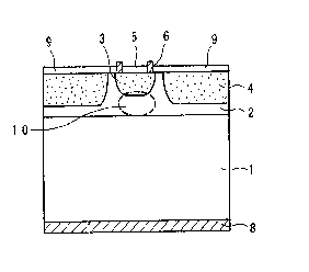
Figs. 3A and 3~ respectively show a basic
structure of a photo-sensing device of the present
invention. Fig. 3A show a top view and Fig. 3B shows
20 ! an X-X sectional view. As shown a semiconductive
crystal layer 2 of a lightly doped first conductivity
type is formed on a surface of a semiconductor
substrate 1 o~ a heavily doped ~irst conductivity type
having an n-electrode 8 formed on an underside thereo~,
and a first region 3 of a second conductivity type is
~ormed in the semiconductive crystal layer 2 by
impurity di~fusion. A pn ~junction area ~ormed by the
.
.
.
.' ,,'- :' ' ' .' ~ ~ . .
~: .
L3~
1 provision of the first region 3 is used as a
photo-sensing region 10. The first region 3 i5
surrounded by the second region ~ of the second
conductivity type ~ormed by the impurity dif~usion A
p-electrode 6 is formed on the ~irst region 3 on the
surface of the semiconductive crystal layer 2, and an
anti-reflection film 5 is formed on the first region 3
inside the electrode 6 while a film 9 is formed on the
semiconductive crystal layer 2 outside the electrode 6.
In the structure such as the above embodiment in
which the semiconductive crystal layer 2 is used as an
i layer of a pin photo-diode, generally, the addition
of the impurities is not performed in the crystal
growth. But the semiconductive crystal layer may
become the first conductive type semiconductor layer by
locally stoichiometric shift in some kind of the
material or by mixture of th0 impurities from a crystal
growing apparatus etc. Further, in order to improve
the electrical characteristics o~ an device, the
impuritles may be added in formation of the
semiconductor crystal layer 2. Therefore, in the
present application, the meaning of "lightly doped"
also includes a case that "the intentional addition of
the impurities is not performed".
When a reverse bias is applied to the
semiconductor device thus constructed, a depletion
layer is created in the pn junction area in the
.
,
: - .
.. . . . .
.
-'- :'
()43~rj
1 semiconductive crystal layer 2. Thus, an electric
field is developed in the depletion layer and electrons
and holes generated by the light directed to the
photo-sensing region 10 are directed to the first
conductivity t~pe semiconductor sub~trate 1 and the
second conductivity type region 3, respectively, and
accelerated thereby. In this manner, a photo-current
is taken out and a light signal is detected. On the
other hand, when the light is directed to the outside
of the phots-sensing region 10, undesired carriers are
absorbed by a depletion layer created by the second
region 4 which is deeply formed in the semiconductive
crystal layer 2. Accordingly, only the photo-current
required for the detection of the light signal can be
taken out. A structure for absorbing the undesired
charges by an impurity layer is disclosed in Japanese
Laid-Open Patent Application No. 96719/1978, it teaches
the provision o~ the impurity layer in order to present
interference between a photo-sensing device and a scan
circuit in an image sensor. However, the improvement
of the response speed which is the object of the
present invention is not attained.
Specific~embodiments based on the above basic
structure are now explained. Figs. 4A and 4B
respectively show a structure o~ a first embodiment.
Fig. 4A shows a top view and Fig. 4B shows an X-X
sectional view. As shown, an n-type InP buffer layer
.: : ,. ~
~5043~
1 2a ~dopant co~centration n = 2 x 1015cm3, thickness 2
~m), an n-type InGaAs (indium-gallium-arsenide)
absorbing layer 2b (n = 2 x 1015cm3, thickness 3,5 ~m~
and an n-type InP window layer 2c (n = 2 ~ 1016cm37
thickness 2 ~m) are ~ormed on a surface o~ an n~-type
Inp (indium-arsenide) semiconductor substrate 1 ln = 2
x 1018cm3) having an n-electrode 8 ~ormed on an
underside thereof. A first region 3 and a second
region 4 of a p type are ~ormed on the photo-sensing
layer 2b and the window layer 2c by selective di~usion
of Zn (zinc) by a sealed ampoule method (impurity
doping method using a sealed silica tube including a
semiconductor wafer and an impurity material). A p-
electrode 6 is formed on the ~irst region 3 in the
semiconductive crystal layer 2, and an anti-reflection
film 5 is formed on the region 3 inside the electrode 6
and a passivation film 9 is formed outside the
electrode 6. An electrode 7 for taking out the charges
collected at the second region 4 is formed on the
semiconductive crystal layer 2.
A band gap energy chart of the pin structure is
shown in Fig. 5. In the present embodiment, the
composition o~ In Ga As o~ the absorbing layer 2b is
InO53~aO47As. This composition provides the smallest
band gap energy, that is, can sense the longest
wavelength light among the InGaAsP semiconductors which
can be lattice-matched with the InP layer.
~O~i~43~
1 It is preEerable that the thickness oE the
absorbing layer 2b is between 1 ~m and 7 ~m to attain
efficient absorption o~ the incident light, although it
is not limited thereto. It is Eurther preEerable that
a width of the n type region between the Eirst region 3
and the second region 4 is between 5 ~m and 30 ~m to
attain good response characteristic and electrical
characteristic, although they are not limited thereto.
In this embodiment, a diameter oE the Eirst region is
100 ~m.
When a light having a wavelength oE 1.3 ~m is
applied to the photo-sensing device thus constructed,
if the light is directed to the outside o-E the
photo-sensing region 10, undesired charges are
collected by the depletion layer created by the second
region 4 deeply Eormed in the semiconductive crystal
layer 2 as described above. When the depth o~ the
second region 4 is deeper than that oE the ~irst region
3, a capturing eE~ect Eor extra charges is higher,
because the extra charges are generated in the
absorbing layer outside the photo-sensing reglon and
di~fuse into the photo-sensing region by the density
graduation. Accordingly, the second region 4 may be
deep enough to reach the buf~er layer 2a. However, it
is~not necessary that the second region 4 is so deep.
For example, when the Eirst region 3 and the second
region 4 are simultaneously ~ormed, they are oE the
.
;~o~ 3~
1 same depth. In this case, the same e~ect as thak of
the present embodiment can be attain. However, when
the second region 4 is shallower than the ~irst region
3, the above e~fect is not attained.
Only the photo-current necessary ~or the detection
o~ the light signal can be take out by the above
structure. The response speed of the photo-sensing
device was measured. As shown in Fig. 2B, the end of
the waveform includes not tail and no degradation of
the response speed by the stray light directed to the
outside of the photo-sensing region lO was confirmed.
In the present embodiment, the incident light has
a wavelength of 1.~ ~m. Since the photo-sensing layer
2b is the In053Ga047As layer, the same ef~ect is attained
for an incident light of a long wavelength such as 1.55
~m.
A second embodiment is now explained with
reference to Figs. 6A and 6B. Fig. 6A shows a top view
and Fig. 6B shows an X-X sectional view. In the
present embodiment, an n-type InO53Ga047As absorbing
layer (n - 1 x 1O15cm3 thickness 5 ~m) is formed, as a
semiconductive crystal layer 2, on a surface of an n+-
type InP substrate 1 having an n- electrode 8 ~ormed on
an underside thereof, and a ~irst region 3 and a second
region 4 of p type are formed by the selective
diffusion of Zn. A diameter of the first region 3 is
300 ~m and a width of an n type region between the
11
.
': , . : '
.
.
,
. . :
.
,
:. . ~
;~S~3~
1 region 3 and the surrounding second regi~n 4 is 20 ~m,
A p-electrode 6 is formed on the region 3 o~ the
absorbing layer, and an anti-reflection Yilm 5 is
~ormed on the region 3 inside the electrode 6 and a
device protection ~ilm 9 is +'ormed on the
semiconductive crystal layer 2 outside the electrode 6.
In the present structure, like the first embodiment,
the charges generated by the light directed to the
outside of the photo-sensing region 10 are collected to
the second region 4 so that the degradation o~ the
response speed is prevented.
A third embodiment is now explained with reference
to Figs. 7A and 7B. Fig. 7A shows a top view and Fig.
7B shows an X-X sectional view. As shown, an n-type
InP bu~fer layer 2a (n = 2 x lOlScm3, thickness 2 ~m),
an n-type InO53GaO47As absorbing layer 2b (n = 2 x 10l5cm
3, thickness 3.5 ~m), and an n-type InP window layer 2c
(n = 2 x lOl~cm3, thickness 2 ~m) are formed on a
surface of an n+-type InP semiconductor substrate l(n =
2 x 10¹³ om3) having an n-electrode 8 ~ormed on an
underside thereof. Further, a ~irst region 3 and a
second region 4 of p-type are formed in the
photo-sensing layer 2b and the window layer 2c by the
selective diffusion of Zn(zinc) by the sealed ampoule
method. A p-electrode 6 is formed on the first region
3 in the semiconductor crystal layer 2, and an
anti-reflection film 5 is ~ormed on the region 3 inside
12
.
~.
' ' . "
' .
~05~ 3~
1 the electrode 6 and a device protection ~ilm 9 i8
formed outside the electrode 6. A metal ~ilm 11 is
formed on the device protection ~ilm ~ to surround the
first region 3. A spacing between the metal filrn 11
and the p-electrode 6 is maintained at 5 ~m.
It is pre~erable that the thickness o~ the
photo-sensing layer 2b is between 1 ~m and 7 ~m in
order to attain efficient absorption o~ the incident
light, although it is not limited thereto. Further, it
10 is pre~erable thak a diameter o~ the ~irst region 3 is
100 ~m, and the width of the n type region between the
first region 3 and the second region 4 is between ~ ~m
and 30 ~m in order to attain good response
characteristic and electrical characteristic although
it is not limited thereto.
In the present structure, since the light directed
to the outside o~ the photo-sensing region is reflected
by the mekal ~ilm 11, the generation of extra charges
is prevented and the degradation o~ the response speed
20 is ef~ectively preYented.
The semiconductor materials and the dimensions
thereof are examples and they change depending on
applications and wavelengths. For example, the
semiconductor materials may be oompound semiconductors
such as GaAs (gallium-arsenide), AlGaAs (aluminum-
gallium-arsenide), CdTe (cadmium-telluride), HgCdTe
(mercury-cadmium-telluride), InSb (indium-antimonide),
. , . . . -
- - : : : ..
: .... . ~ ~ : ,
' ' :. ' ' '
.
-:
:
~0~04~
1 or Si (silicon) or Ge (germanium). The impurity
di~fusion may be done by an ion implantation method.
In accordance with the present .invention, the
degradation o~ the response speed is prevented by the
simple means of depleting a portion oY the light,
absorption region around the photo-sensing region and
collecting the charges generated by the light directed
to the outside of the photo-sensing region, and the
highIy sen-sitive photo-sensing device is provided.
From the invention thus described, it wlll be
obvious that the invention may be varied in many ways.
Such variations are not to be regarded as a departure
from the spirit and scope o~ the invention, and all
such modifications as would be obvious to one skilled
in the art are intended to be included within the scope
of the following clai-s.
~
~;
.
''' ': : ' , , , :
',~ ~ ~ ' ' '
'~''''~ ' ~ ' , '