Note: Descriptions are shown in the official language in which they were submitted.
7~
1 Title o~ the Invention
SEMICONDUCTOR ELEMENT MANUFACTURING PROCESS
Back~round o~ the Invention
(Field o~ The Invention)
The present invention relates to a method o~
manu~acturing a semiconductor device and more
particularly relates to a treatment o~ a back sur~ace
of a GaAs substrate on which a semiconductor device is
formed.
(Related Background Art)
A semiconductor element ~ormed on a GaAs
Substrate, a chemical compound semiconductor, haæ a
di~iculty to dissipate heat generated from the device
formed on a sur~ace o~ the GaAs substrate, since
thermal conductivity of GaAs is 1/3 times as low as
that of Si. It adversely a~ects characteristics o~
the device. And, it is necessary to thin the substrate
and assure a good dissipation o$ heat. On the other
hand, GaAs lS brittle compared with Si and easy to be
cracked and/or broXen of~. So, chip cracking is easily
caused starting ~rom ~ine flaws and the like yielded at
a thinning process. Therefore, mirror sur~ace ~inish
has been conventionally adopted with a grinding stone
having ~ine grain sizes (See "THE IMPACT OF WAFER BACK
SURFACE FINISH ON CHIP STRENGTH" o~ IEEE/lRPS). And,
an application ~iled by the assignee and inventor o~
,~ . , .
:
.
~S~i7~i
l the present invention on Dec. 5, 1986 also disclosed
that GaAs substrate has the maximum strength after
die-bonding when back ~inish (R max) o~ the substrate
is somewhat between 0.2 and 0.~ micro-meters. It is,
however, di~ficult to obtain R max in this region only
with grinding. And, in the prior art, mirror grinding
has been used to obtain R max of 0.1 micro-meters or
~iner to eliminate ~ine ~laws, consequently preventing
a chip ~rom being cracked.
A grinding stone with ~ine grains, however, must
be used to perform the a~orementioned mirror grinding.
It means only a small amount to be ground o~f per a
unit time and taking a long time o~ period to grind
off a predetermined amount. It results in low
productivlty ~or mass production and in making a
process complicated because of a need o~ ~acilities ~or
mirror grinding.
Summar~ o~ the Invention
In view o~ the above mentioned circumstances, it
is an object o~ the present invention to provide a
semiconductor device manu~acturing process, wherein a
back treatment can be per~ormed in a short time of
period and also semiconductor device can be
manu~actured with minimum chip cracking.
It i8 further object o~ the present invention to
provide a method o~ manu~acturing a semiconductor
- :: ;: :
:
.:
::
.
~S~
1 device comprising the steps o~: ~orming a semiconductor
element on one o~ ma;or sur~aces o~ a GaAs substrate;
a grinding the substrate ko make the ~aAs substrate to
a predetermined thickness by gri.nding the other sur~ace
of the GaAs substrate with a grinding stone having an
average grain size o~ 6 micro-meters or larger; and an
chemical etching the other sur~ace o~ the substrate by
0.6 micro-meters or more just after the grinding step,
without any ~urther grinding treatment done on the
other sur~ace, just a~ter the grinding step.
In a method according to the present invention, a
grinding stone with a grain size o~ 6 micro-meters or
larger is used to grind a GaAs substrate, on which a
semiconductor element is formed, in a short time o~
period. And therea~ter a chemical etching removes a
deformed layer on a back sur~ace o~ the substrate
caused by the above mentioned grinding step. It
enables to manufacture a GaAs substrate with high
strength, in a short time o~ period.
The present invention will become more ~ully
understood ~rom the detailed desoription given
hereinbelow and the accompanying drawings which are
given by way o~ illustration only, and thus are not to
be considerrd as limiting khe present invention.
Further scope o~ applicability o~ the present
invention will become apparent ~rom the detailed
description given hereina~ter. However, it should be
. . - , .
~ :
:"
)t~7~
1 underst,ood that the detailed description and speci~ic
examples, while indicating pre~erred embodiments o~ the
invention, are given by way o~ illustration only, since
various changes an~ modi~ications within the spirit and
scope of the invention will become apparent to those
skilled in the art form this detailed description.
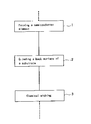
Brie~ DescriPtion _f the Drawin~s
Fig. 1 shows a summarized ~low chart o~
characteri~ing portions o~ an embodiment according to
the present invention;
Fig. 2 is a graph showing relation between grain
size o~ grinding stone and ~inish sur~ace roughness R
max; and
Fig. 3 is a graph showing relation between amount
o~ etching and sur~ace condition factor K o~ the back
surface o~ GaAs substrate.
Description o~ the Pre~erred Embodiment
Re~erring to Drawings, an embodiment according to
the present invention is explained as ~ollows.
As shown in Fig.l, the characterizing process is
comprised o~ step 1 o~ ~orming a semiconductor element
on a sur~ace of the GaAs substrate, step 2 of grinding
o~ a back side o~ the GaAs substrate on which the
semlconductor element is ~ormed, and a step 3 oi
per~orming chemical etching to remove the back side by
:: . ~
36~
1 a predetermined thicknees, ~ust a~ter the grinding
step
Concretely, a semiconductor ~lement is ~ormed on
one o~ mai~ sur~aces o~ the GaAs wa~er Yirst. The
semiconductor element is, ~or example Shottky-gate type
~ield e~ect transistor or the like and on the one main
sur~ace, monolisic microwave integrated circuit or the
like is ~ormed by such ~ield e~ect transistors.
This step is performed utilizing photo-lithograph
technique, ion implantation technique and the like.
These are not described in detail here, as
conventionally well known.
Secondly, the one sur~ace o~ the GaAs wa~er on
which the semiconductor element is ~ormed is completely
covered with a ~ilm made o~ organic material etc. and
therea~ter the wa~er is mounted on a grinding machine
by holding the covered surface thereo~ on a rotational
stage of the grinding machine to grind the back side
sur~ace of the wa~er. In the grinding, that is a so
called as a back grinding, the rotational stage
mounting the wa~er thereon is rotated and forwarded to
a grinding stone rotating and located so as to ~ace to
the rotational stage and as the result the back side o~
the waYer is made in conkact with the grinding stone to
be ground. Usually, a wa~er rotation down-~eed method
is used, as grinding resistance can be l~ept constant in
it. And a diamond grinding stone with an average grain
- ' '
~ ~ .
~ '7~,9
1 size o~ 6 micro-meters or larger is used. The reason
why the average grain size oY 6 or larger is adopted is
that grinding speed would drastically decrease with a
smaller grain size because the ~inish must be o~ mirror
grinding. And, in case o~ the average grain size o~ 6
micro-meters or larger, sur~ace ~inish roughness (R
max) falls under approximately 1. This roughness
enables the sur~ace to be ~inished to nearly a desired
value (0.2 to 0.5 micro-meters) with the chemical
etching treatment ~ollowing the prior grinding
treatment. Fig.2 shows a relation between an average
grain oY a diamond grinding stone (horizontal axis) and
a roughness (R max) (vertical axis) in the sur~ace to
be ~inished. As shown in Fig. 2, when the a~erage
grain changes ~rom 6 micro-meters to 25 micro-meters,
in response to the change, the roughness changes ~rom
O.q micro-meters to 3 micro-meters. Further in about 6
micro-meters o~ the average grain, the amount o~ R max
changes incontinuousiy. This shows that 6 micro-meters
in a size o~ the average grain is critical value.
Generally, such incontinuous change in R max can not be
observed in the grinding in Si wa~er and such
incontinuous change was also observed by a scanning
electron microscope.
Next, the back surface o~ the wa~er is chemically
etched without any ~urther grinding treatment. In the
chemical etching step 3, the side o~ the GaAs substrate
, - , .
.
.
- ~ .-
.
,
~ O S~7
1 on which the semiconductor element is ~ormed is covered
with a protection ~ilm, be~ore the substrate is soaked
in a mixture o~ ammonia, hydrogen dioxide and water
l'he mixture should have a very low etchi~g speed. An
example o~ the mixing ratio o~ such a mixture is
NH40H : H~02 : H20 = 1 : 1 : 10, and the substrate is
soaked in it ~or about 20 seconds. Various liquid
mixture can be used as an etchant, ~or example,
phosphoric based etchant, potassium-hydroxide based
etchant or aqua regia etc. The step chemically etches
the back surface o~ the GaAs wa~er by 0.6 micro-meters
or more.
The amount o~ etching should be 0.6 micron-meters
or more because the thickness o~ the de~ormed layer
yielded on the back surEace of the GaAs wa~er by the
previous grinding is about 0.6 micro-meters. A bend or
the like in the wa~er can be satis~actorily removed
only by removing the de~ormed layer. Fig. 3 shows a
relation between etching amount and sur~ace condition
20- factor(K) on the back surface of the substrate, and the
sur~ace condition ~actor corresponds to a bend degree
o~ the wafer. The relation shown in Fig. 3 proves the
etching amount is su~ficient, because K value is
restored to the same level as that o~ polished sur~ace
at 0.6 micro-meters etching (See "Technique o~ GaAs
wa~er mirror grinding" in Super-Precision Machining
manual). In Fig.3, a broken line shows polished
1 sur~ace, white dots non-mirror grinding (rough
grinding) and ~illed dots mirror grinding respectively.
Semiconductor elements were manu~actured by the
above method and the Die~Shear Skrengkh was compared
between following two cases:
(1) mirror grinding the back sur~ace o~ the wa~er
to make R max to be 0.1 micro-meters and therea~ter
etching it by 0.1 micro-meters; and
(2) rough grinding the back sur~ace o~ the waYer
to make R max to be 1 micro-meter and therea~ter
etching it by 0.6 micro-meters.
And it was observed that the strength was 1.5
kg/mm in the both cases. In addition, no cracking was
caused in a 5 x ~mm chip by 1000 cycle thermal impact
o~ -65C to +150C, with 0.6 micro-meter etching even
in case that R max was 1 micro-meter.
Further, the applicant (inventor) measured "the
Fracture Stress" o~ GaAs substrates respectively
manu~actured by the following two methods 1 and 2, by
two di~erent methods, one is a so-called "Four-Point
Loading method" and the other is a so-called "Biaxial
Loading method",
(1) Method 1, Which is corresponding to a
conventional method: Rough-grinding, Mirror-grinding
and chemical etching are applied to a back sur~ace o~
the substrate.
(2) Method 2, Which i~ corresponding to a method
. ~ , . .
. ,: - . . . .
. ~ . ,
: ~ .
-
, : :
-
., '
~5~
1 according to the present invention;
Rough grinding and chemical etching are applied to
a back sur~ace o~ the substrate without the application
o~ Mirror grinding. Table I shows "Fracture Stress
data" obtained by the Four~point Loading method and
Table II shows "Fracture Stress data" obtained by the
Biaxial Loading method.
TABLE I
FRACTURE STRESS DATA FOR FOUR-POINT LOADING
1 0
Manu~acturing Thickness Mean Fracture Weibull
method Stress Modulus
1 450 ~m 163 2.2
1 300 ~m 156 3.B
1 200 ~m 181 Z.4
2 450 ~m 182 3.3
-2 300 ~m 173 3.4
2 200 ~m 163 7.3
2 140 ~m 154 2.1
::
:
~: :
g
~:
. . . .
~ '
, ~ .
~ .3
1 TABLE II
FRACTURE STRESS DATA FOR BIAXIAL LOADING
Manu~acturing Thickness Mean Fracture Weibull
method Stress Modulus
1 450 ~m 187 3.1
1 300 ~m 179 2.5
1 200 ~m 199 1.9
2 450 ~m 129 5.5
2 300 ~m 110 9.9
2 200 ~m 102 5.8
2 140 ~m 114 6.4
The above results shown in the tables I and II was
published in a paper titled as "High Mechanical
Reliability o~ Back-ground GaAs LSI Chips with Low
Thermal Resistance" on pages 890 to 896 in Proceedings
o~ the 41st Electronic Components and Technology
Con~erence (ECTC) held on May 13 to 1~, 1991 at Atlanta
in U.S.A., by the applicant (inventor) the present
invention.
As shown in the tables I and II, Fracture Stress
data of the substrates manu~actured by the two method 1
and 2 are substantial equal to each other. There~ore,
it can be understood that the substrate manu~actured by
the method 2 has the substially same strength as that
o~ the substrate manu~actured by the method Z.
A~ter the above chemical etching, GaAs wa~er is
divided into individual IC chip by a dicing machine.
.
','' '` ' ' ~':
9~Jt;~
1 The divided IC chip is die bonded on a ceramic plate by
an eutectic alloy using AuSu etc. Besides, be~ors the
die bonding, the back surface o~ the GaAs is metalized
by Ti evaporation etc. and further Au layer is
deposited thereon.
As described above, according to the present
invention, a combination o~ the high speed grinding and
the chemical etching enables a semiconductor element
with su~iciently strong GaAs substrate to be
manu~actured in a short time o~ period.
Additionally, mirror grinding treatment can be
eliminated, which simpli~ies manu~acturing facilities
and shortens manufacturing time. Consequently the
present invention enables the semiconductor element to
be manu~actured at a low cost.
From the invention thus described, it will be
obvious that the invention may be varied in many ways.
Such variations are not to be regarded as a departure
~rom the spirit and scope o~ the invention, and all
such modi~ications as would be obvious to one skilled
in the art are intended to be included within the scope
o~ the ~ollowing claims.
11
,