Note: Descriptions are shown in the official language in which they were submitted.
~~~~~'~~
DUAL MODULUS COUNTER CIRCUIT
FIELD OF THE INVENTION
The present invention relates generally to a
programmable divider for use in a digital frequency synthesizer.
More particularly, the invention relates to a dual modulus
counter suitable far controlling the programmable divider.
BACKGROUND OF THE INVENTION
In digital frequency synthesizers, there is a need for
a variable divider cahich counts the cycles of an input signal
having a given freguency until a predetermined number of counts
have been accumulated. The size of the count is usually referred
to by the letter N. Once N counts have been accumulated, the
variable divider is reset to begin the cycle again. It is
desirable for the number of counts N to be variable in order that
~.5 it can be programmed in advance of each count by means of a
control input.
When N is large and the operating frequency of the
counter is vto be high, technical difficulties can arise in
constructing a multistage high frequency variable divider. In
he prior art, the problem is typically overcome by using a fixed
high frequency divide by M stage prior to a variable divide by
N stage. This solution is not always desirable because the total
division factor can only be a multiple of M.
In a digital frequency synthesizer application, it is
usually desirable to be able to program the total division
factors in steps or increments of 1. The steps, therefore,
relate to the frequency resolution or the frequency step size of
~~~~f~'~~_ .
-2-
the synthesizer. If the divider is only programmable in steps
of M, the frequency steps available are relatively coarse and
determined by the factor M.
Another approach to the problem is to begin with a high
frequency divider stage or prescaler while retaining the ability
to program the divider count cycle length in steps of 1. This
arrangement allows the prescaler to be varied between dividing
ratios of R and R+1.
It is possible, for example, for a dual ratio prescaler
having the division ratios 10 and 11 to perform a division of
157. The number 157 can be expressed by the equation 7x11-1-(15
7)x10. The prescaler is first programmed to divide by 11, and
the lower frequency divider stage is set to count 7 prescaler
output pulses. After counting 7 prescaler output pulses, the
prescaler is set to divide by 10. The low frequency divider
stage is then set to count 8 prescaler output pulses. Upon
completion of this count, a total of 7x11+8x10=157 input pulses
have been applied to the prescaler input. The cycle is then
begun again. It should be noted that in order to obtain numbers
in steps of 1, the number of times the prescaler divides by 11
must be programmed from 0 to 9 and the number of 10's in the
total number must not be less than 9. This relationship sets a
lower bound of R(R-1) for the contiguous number range that can
be achieved with a two ratio prescaler having ratios R and R+1.
The most common method employed to count two different
numbers of prescaler output pulses, N1 and N2, while the
prescaler is dividing respectively by ratios R1 and R2, is to use
two separate low frequencydown counters that are preset to the
-3-
values N1 and N1 + N2, respectively. For example, the division
of 157 with the aid of a 10/11 prescaler could be achieved by
presetting one divider to N=7 and the other to N1+N2=15. The
prescaler would then first be set to divide by R1(11) while both
low frequency counters counted down on the prescaler output
pulses. When the N1 counter reaches zero after 7 prescaler
output pulses, the prescaler would switch and divide by 10, and
the N2 counter would continue to count down a further 8 prescaler
output pulses until it reaches zero, completing the cycle. This
system has the advantage that a desired division number is simply
expressed in values to which the N1 and N2 counters can be
preset. This arrangement has the disadvantage that two variable
dividers are required and power consumption is increased when
both dividers are operating. Increased power consumption is a
significant disadvantage for battery powered equipment.
U.S. Patent No. 4,053,739 describes a single variable
divider that is alternatively programmed with the value N1 when
the prescaler divides by the value R1 and :is programmed :with the
value N2 when the prescaler divides by the value R2. This device
has the advantage that a single variable divider suffices.
Unfortunately, the described arrangement includes additional
circuit complexity in the form of a multi-line switch. The
multi-line switch alternately selects the bits corresponding to
the values N1 and N2 in order to preset the single variable
divider. Although this additional circuitry operates at a lower
power consumption than a circuit having two variable dividers,
it still requires substantially the same amount of circuitry when
implemented as an integrated circuit.
~~~~~'~
_4_
Accordingly, there is a need for a counter for a
programmable divider which can register both the.counts N1 and
N2 without them being presented alternately to the counter. This
arrangement would eliminate the need for a complex mufti-line
switch.
SUMMARY OF THE INVENTION
The present invention relates to a circuit and method
for controlling a programmable divider for use in a digital
frequency synthesizer. The programmable divider is responsive
to a dual modulus counter. The dual modulus counter includes a
preloadable binary counter, a comparator and logic gates which
generate selection signals to control the programmable divider.
The preloadable counter is loaded with a value N1. The counter
counts to a predetermined intermediate value such as zero and
generates an output signal. The counter then continues to count
until it reaches a second value N2. The comparator compares the
output'of the counter to the value N2 which was loaded into the
comparator. When the binary counter reaches the value N2, the
comparator generates a second output with is applied to the logic
gates. The logic gates generate the selection signals which
cause'the programmable divider to divide an input signal by the
division ratios R1 or R2. In a first embodiment of the present
invention, the bznary counter is a down counter. In a second
embodiment of the present invention, the binary counter is an up
counter. The dual modulus counter of the present invention may
also be used to control more than one programmable divider. The
present invention is particularly well suited for use in a
~~D~~f~'r
-5-
digital frequency synthesizer of the type having a phase locked
loop.
BRIEF DESCRTPTION OF THE DRAWINGS
Fig. 1 is a schematic diagram of the first embodiment
of the present invention having a binary down counter;
Fig. 2 is a schematic diagram of a second embodiment
of the present invention having a binary up counter;
Fig. 3 is a schematic diagram of the dual modulus
counter of the present invention controlling two programmable
to dividers; and
Fig. 4 is a schematic diagram of a phase locked loop
utilizing a variable divider.
DETAILED DESCRIPTION OF THfE INVENTION
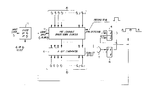
Fig. 1 illustrates a schematic diagram of the first
embodiment of the present invention. In the first embodiment,
there is shown a dual modulus counter having a binary down
counter l2 which is loaded at the beginning of a count sequence
with the value N1: There is a prescaler 11 which can divide by
the ratios R1 or R2. The output pulses of the prescaler 11
decrement the down counter l2 until the down counter reaches the
value zero. When the down counter l2 reaches zero, it generates
an output pulse which sets a latch 14. The setting of the latch
14 causes the prescaler l2 to switch to its alternative division
ratio R2. The output pulses of the prescaler 11 continue to
decrement the down counter 12 until a comparator 13 detects that
it has reached the state carresponding to a value -N2. When the
~~~~E~
-6-
comparator 13 detects the value -N2 , the latch 14 is already set,
and both inputs to an AND gate 15 are enabled. The AND gate 15
then generates an output signal which is clocked into a d-type
flip flop 16 upon the next prescaler output pulse. The latch 14
is then reset, and the down counter 12 can be reloaded with the
value N1, while the prescaler 11 resumes division by the ratio
R1.
Since the inputs to the AND gate 15 are no langer
enabled because the latch 14 has been reset, the output signal
at the AND gate 15 will disappear and this state will be
transferred into the d-type flip flop 16 upon the next output
pulse of the prescaler 11. The preset control signal to the down
counter 12 is removed leaving it loaded with the value N1 and
ready for the next count sequence. The total number of prescaler
input pulses in the count sequence, therefore is expressed by the
equation NTOT-(N1+1)R1+{N2+1)R2. In order to obtain a desired
NTOT, it is necessary to subtract the excess R1+R2 value from the
desired number. For example, if R1=11 and R2=10, and a total
division cycle length of 170 is desired, 10+11=21 is first
. 20 subtracted from 170 resulting in the value 249. N1 must then be
9 and N2=14-9=5. In order to avoid impossible negative values
of N2 arising, a desired count N must satisfy the following
equations:
INT {(N-R1-R2)/R2) >_ IN-R1°R2~R2
INT { (2d-R1-R2 ) /R1 } >_ ~ N-R1-R2 ~ R~
The expression INT (x) means the whole number part of x, i.e.,
if x = 5.3667, then INT(x) - 5. This is an expression of the
above-described lower bound on the contiguous number range that
~~~~~
_~-
can be spanned using the dual ratio prescalers associated with
the present invention.
In the circuit illustrated in Fig. 1, there is no
restriction placed on the relative magnitudes of N1 and N2. The
word length of the comparator 13 was the same as the whole number
in the counter 12. However, to cover a range of values of N in
steps of 1 with no gaps only requires that Nlt1 take on values
between 1 and R1-1, i.e., the range of the least significant
digit of N modulo R1. Since this range is often much shorter
l0 than the total length of the counter 12, the comparator 13 word
length can be advantageously reduced. The reduction of the word
length of the comparator 13 can be achieved by using an up
counter:
Referring now to Fig. 2, a second embodiment of the
present invention using an up counter is illustrated. In the
second embodiment of the present invention, there is a
preloadable binary up counter 22 that ins responsive to the output
of a prescaler 21. The prescaler 21 is capable of dividing by
division ratios R1 or R2. The up counter 22 is initially preset
to a value -N1, while the prescaler 21 is initially set to divide
by Rl. The output pulses of the prescaler 21 increment the up
counter 22 until the output of the up counter reaches all logical
ones. When the output of the up counter 22 is all logical ones
instead of all logical zeros, the output can be more rapidly
detected.
Upon detecting all logical ones, a latch 24 is set
causing the prescaler 21 to switch to division by the ratio R2.
If N2 equals 111..1, an L-bit comparator 23 provides an output
~05~~
_8_
signal to an AND gate 25. The AND gate 25 generates an output
signal. Otherwise the L-bit comparator 23 generates an output
signal after one further output pulse from the prescaler 21 if
N2=0, after two output pulses if N2=1, etc. On the immediately
following prescaler output pulse, the output of AND gate 25 is
clocked into a d-type flip flop 26 causing the latch 24 to be
reset. The prescaler 21 returns to dividing by R1, and the up
counter is reloaded with the value -N1. Since the resetting of
the latch 24 removes one of the enabling inputs to the A3dD gate
25, the output of the AND gate becomes 0. This output is
transferred to the d-type flip flop 26 on the next prescaler
output pulse, thereby removing the reload control signal to the
up counter 22 and leaving it in the state -N1 and leaving it
ready to repeat the entire cycle.
The total number of prescaler input clock pulses in a
complete division cycle for the circuit: of Fig. 2 is defined by
the equation N=NlxR1+(N2+2)xR2. It should be noted, however,
that the value N2=-1 is correctly treated by the circuit, so that
N2 is considered to range through the values -1, 0, +1 ..: to
2**L-2. The value N2' is defined by the equation N2'=N2+1 and
ranges from the value 0 to 2~-1. The value N is defined by the
equation N=NlxR1+N2'xR2+R2. The values for N1 and N2' may be
calculated as follows: (1) Subtract the excess R2 from N to get
N' , (2) calculate N2' as the remainder upon division of N' by R1,
(3) calculate N1 as the integer part of N'/R1-N2', and (4) apply
N2=N2' -1 to the L-bit comparator 23 and N1 to the divider preload
input of counter 22. These manipulations can be performed more
simply if the value R1 is a power of 2.
~~~ d ~D
-9-
Referring now to Fig. 3, a schematic diagram
illustrates a plurality of programmable dividers or prescalers
30, 31 being controlled by the dual modulus counter of the
present invention. Two digital comparators 35, 36 are used to
examine the state of the least significant L-bits of a main
counter 37. After counting up from a value -N1 to an all logical
ones condition, the comparators 35, 36 in turn detect when the
least significant bits of the main saunter 37 becomes equal to
N2 and then to the value N3. These events cause the prescalers
30 and 31 respectively to divide by their alternative ratios.
For example, suppose the prescaler 31 has the ratios 10 and
11 available, while the prescaler 30 has ratios of 9 and 10
available. Assuming that 'the flip flops 38, 39 and 40 axe in the
reset condition, both prescalers 30, 31 begin by dividing by 10.
The counter 37 then counts up from -Na. until its output is all
logical ones. The latch 38 then becomes set, causing the
prescaler 31 to divide by 11. The counter 37 continues to count
up until the comparator 36 detects a state corresponding to the
value N2. If latch 38 is also set, both inputs to an AND gate
41 are enabled and the latch 39 is set. This causes the
prescaler 30 to begin dividing by 9 while the prescaler 31
continues to divide by ll. The counter 37 continues to Count
until the comparator 35 detects a bit state corresponding to the
value N3. At this point; if latch 39 is already set, both inputs
to the AND gate 42 are enabled and upon the next output pulse
from the prescaler 31 the output signal of the AND gate 42 is
clocked into the flip flop 40, causing the latches 38, 39 to be
reset and the reloading of the main counter 37 to the starting
~a~~~~~d ~a
-10-
state N1. The prescalers 30, 31 are now back in their original
divide by 10 condition, and the inputs to the AND gate 42 are no
longer enabled. After one more pulse from the prescaler 31, the
zero signal from the AND gate 42 is transferred into the flip
flop 40 removing the reset condition and leaving the counter 37
in the state -N1 and ready to start a new cycle.
The total cycle length in terms of output pulses of the
input clock signal F~ can be expressed by the following equation:
N=100N1+110(N2+1)+99(~N3-N2~+1)
where the absolute value of N3-N2 corresponds to modulo 2**L,
where L is the number of least significant bits of the counter
37 examined by the comparators 35, 36. The value N3° is defined
by the equation N3'= ~N3-N2~. The value of N, therefore, can be
defined by the following equation:
N=100(N1+N2)+110(N2+1)+10N2-N3'+209
A desired count may be produced in the following fashion, (1)
subtract the excess 209 from the desired count, getting N', (2)
round up N' to the next multiple of 10, which is called N°', (3)
Set N3' t~ (N"-N'), (4) set N2 to the 10's digit of N", arid (5)
- 20 set Nl to the loo's digit of N°-N2. Far example, suppose
N=1,568. Then N'=1,568-209=1,359. N"=1,360. N3'=N"-N'=1.
N2=6(10's digit of N"). N1=13-N2=7(100's digit N"-N2). Because
of the subtraction of N2 from the number of loo's in N'° and the
value of N2 ranges up to 9, the number of loo's in N°° can not
be
less than 9. Therefore, the lower bound on the contiguous number
range is of the order of 900/(209-9)=1,100. This is an order of
magnitude lower than the lower bound of 9,900 that would apply
for a two-ratio prescaler of ratios 100 and 101. In general, an
~~~~'a''~$'~ ..
-11-
advantageous way to obtain a total frequency reduction of the
order of R**2 from the input clock signal F~ to the input of the
low frequency divider is to use two prescalers having the ratios
(R, R+1) and (R, R-1) respectively.
The principles of the present inventions may be
extended by adding additional comparators as necessary. The
comparators are not constrained to be of the same word length and
bits, nor are the prescalers they control constrained to exist
separately. The two prescalers 30; 31 of Fig. 3 can also be
regarded as a single circuit having three or more division ratios
selectable by two or mare control lines. Such an arrangement can
be advantageous because the exact moment at which the highest
frequency prescaler 30 is switched between its ratios can be more
time critical than the lower frequency logic can define. It is,
16 therefore, possible that a necessary precaution is to retime the
control signal to the highest frequency prescaler with the logic
having substantially the same speed as prescaler 31.. The control
signal from the low speed logic, therefore, should preferably
pass through the medium speed prescaler 32 to be retimed more
accurately. This will have a small penalty on the lower bound
of the contiguous number range that the overall division ratios
can span, but it will increase the maximum frequency of operation
before timing problems are encountered.
The prescaler division ratios of the present invention
are not constrained to any particular values. Common values that
simplify the calculation of the values N1, N2, and N3 can be
based on either a decimal number system or a binary number
system. In cases where the ease of calculation is not an issue,
-12-
such as when adequate microprocessor capability exists or number
radix manipulations or when precomputed lookup tables can be
used, it may be possible to find other advantageous combinations
of prescaler ratios, e.g. noncommesurate primes.
Referring now to Fig. 4, a schematic diagram
illustrates the use of the present invention in a phase locked
loop. The phase locked loop includes a voltage controlled
oscillator 50 which provides an output signal Fo. The output
signal Fo is applied to a variable divider circuit 51. The
variable divider circuit 51 includes a programmable divider and
the dual modulus counter of the present invention. The total
division ratio N of the variable divider circuit 51 is a function
of the values N1 and N2 associated with the dual modulus counter.
The output of the variable divider circuit 51 is a divided output
signal Fo/N which is applied to a phase comparator 52. The phase
comparator 52 compares 'the phase of the divided output signal
Fo/N to a divided reference frequency signal F~/M. The divided
reference frequency signal is produced from a reference clock
signal that is divided by a digital divider 53. The output of
the phase comparator 52 is a signal representative of the phase
error. The phase error signal is applied to a loop filter/
integrator 54. The filtered and integrated output is then
applied to the voltage controlled oscillator 50.
While the invention has been described in its preferred
embodiments, it is to be understood that the words that have been
used are words of description rather than of limitation and that
changes within the purview of the appended claims may be made
~~ a~~'~
-13--
without departing from the true scope and spirit of the invention
in its broader aspects.