Note: Descriptions are shown in the official language in which they were submitted.
~ '~' ~----`'~ ~ ~1~ ~UU~y
P~J8H--p~T~T- OPTIt~T. RE~.; ei l V~SK 2 0 5 ~ ~; 8 0
Tec~nical Field
The present invention relates to optical transmission
systems and more particularly to an optical receiver with
5 improved dynamic range for receiving optical signals amplitude
modulated with wi ~h~~ video signals.
B~c~ro~n~ Art
In recent years, there has been a great deal of interest
in the trAn~miccion of video signals via optical fiber. This
mode of signal tr~C~ ion offers a number of advantages over
transmitting signals over conventional 75 ohm coaxial cable
15 as video signal distribution is now commonly accomplished in
CATV systems. Optical fibers intrinsically have more
information-carrying capacity than do coaxial c~bles. In
addition, there is less signal attenuation in optical fibers
than in co~Yi~l cable adapted for carrying radio frequency
20 signals. Co~^quently, optical fibers can span longer
distances between signal regenerators than is possible with
coAY;~l cable. In addition, the dielectric nature of optical
fiber eliminates any problems with electrical shorting.
Finally, optical fiber is immune to ambient electromagnetic
25 interference (EMI) and generates no EMI of its own.
Amplitude modulation of an optical signal with a wideband
radio frequency signal requires a light modulating device,
such as a laser, which has linear characteristics of a wide
dynamic range of operation.
30Until recently it has been difficult to fa~ricate lasers
in which the relationship between input current and optical
ouL~u~ was li~r over more than an extremely limited range.
Because of this difficulty in obt~i n i ng lasers which were
sufficiently linear to support analog amplitude modulation,
35 digital modulation was, until recently, the primary means for
transmitting information by optical signals. Digital
modulation does not require a laser with a large dynamic range
as do analog means for transmitting information (e.a.
- amplitude modulation or frequency modulation of a carrier
40 frequency modulating the laser o~L~hL). Digital modulation
- v ~ JO l~ l / U~
5 ~ ~ 8 1~ 2
of the laser offers high signal quality and is also compatibl
with telephone trunk and feeder networks. However, because
of the wideband nature of video signals digitization of these
signals consumes extremely large amounts of channel capacity.
5 A typical video signal occupies 6MHz of bandwidth.
Transmission of this information digitally required a digital
data transmission rate of approximately 45 megabits per
-?~Q~. High definition video (HDTV) may reguire a digital
data transmission rate of up to 145 megabits per second.
10 Moreover, e~o~rs and ~co~rs for converting ~nalog video
signals to digital form and for reconverting these digital
signals to analog form for viewing on a conventional
television set are quite eYr~ncive. Consequently, analog
transmission of video Fignals is potentially much more
15 economical than digital transmission of such signals.
~ ecent advances in laser te~hnDlogy have made analog
modulation of optical ~ignals feasible. Currently available
Fabry-Perot (FP) and Distributed ~eedback (DFB) lasers have
sufficiently linear characteristics to ~llow them to be used
20 as analog modulators of optical signals.
One ~uch means of analog tr~nsmission is to use the
hA~eh~ television signal to frequency modulate a radio
frequency carrier. This modul~ted radio frequency carrier is
in turn used to modul~te an optical signal. Such freguency
25 modul~tion is less rn~-ertible to noise than is amplitude
modulation but it reguires more bandwidth for each television
~h~n~el transmitted than ~re required by amplitude modulation
method~. Thus, the number of television ~h~nnel ~ which can
be carried by each optical tr~nsmission (e.a., ~ch optical
30 fiber) in an FM-ba~ed ~y~tem may be somewhat limited.
Moreover, since the st~nA~rd NTSC format for video calls for
amplitude modulation of the video carrier, means for
converting FM signals to an NTSC amplitude modulated fo~mat
are required either at the television receiver or at the point
35 at which the fiber transmi~sion trunk is co.~ Led to a
coAYi~l cable distribution network. The need for such F~ to
NTSC AM conver~ion increases the cost of the system.
In view of the above, a ~ystem in which the video
hAFsh~n~ signal amplitude modulates a radio frequency carrier
40 signal which in turn amplitude-modulates an optic~l ~ignal is
preferable to other ~ystems from the stAn~roint of cost and
simplicity. However, several phenomena limit the number of
radio frequency chAnnel~ which can be carried by present day
optical links where the intensity of light signals is
- 2 0 5 0 6 8 0
amplitude modulated. A first of these phenomena is a
limitation of the amount of radio frequency energy which may
be supplied as a modulating signal to a laser or other light
generating device before various types of distortions are
5 generated by the light generating device. This power
limitation relates to the sum of the radio frequency power
contributions of each radio frequency channel. Thus, if it
i5 desired to transmit 80 radio freguency channels over a
single optical link, the power available for each channel is
lo only half of the power which would be a~ailable if only 40
ch~nnel~ were transmitted by the optical link. Such a
limitation on the power of each radio frequency carriar brings
each of these carriers closer to the "white noise" level of
the system, thus, adversely affecting the signal to noise
15 ratio of the syste~, Decreasing the nl~mher of channels
carried by each Opti~al link in order to improve the signal
to noise ratio increases the number of lasers which must be
used and the overall complexity and cost of the system. on
the other hand, increasing the amount of radio frequency power
20 supplied to the laser beyond certain limits may cause the
laser to produce several types of distortion which are
~;~C~ below.
When the modulating signal ~upplied to a laser causes the
laser to be driven into a nonlinear portion of its input-
25 signal-to-light ouL~uLcharacteristic,harmonicdistortionmay
be produced. The products of this type of distortion are
signals which are integer multiples of the "primary"
frequency. The -ec-n~ harmonic of 54MHz is, for example,
108NHz. Thus, if the bandwidth accommodated by a system is
30 such that there are chAnn~ls at both 54MHz ~nd 108MHz, second
harmonics of the 54MHz ~hAnnPl will interfere with the signals
on the 108MHz chnnnel.
Intermodula~ion distortion is also of particular concern
in ~mplitude modu~ted systems. Such distortion results in
35 distortion produc~s at frequencies which are the sum or
difference of two other frequencies. The distortion products
are the sum difference of two primary freguencies are called
~e-Qn~ order distortion products and ~re particularly
troublesome. For example, a video chAn~el at 150MHz and
40 another video ~hAn~el at 204MHz may produce a ~eCQ~ order
dis.ortion product at 54MHz (the difference frequency) and at
354MHz (the sum frequency). Third order distortion products
are produced by the mixing of a primary frequency with a
~~con~ order distortion product. This pro~cee third order
tt, r~ Yl/Wy~
~ ~oSQ68~ 4
dIstortion products at the sum and difference between th
primary frequency and the frequency of the 6econd order
distortion product. Third order distortion products may also
be generated b~ mixing signals at three frequencies or by
5 third harmonic generation.
Clearly, one method of dealing w~th the above problems
is to utilize detectors and amplifiers which are highly linear
and which are thus relatively insusceptible to harmonic and
intermodulation distortion. It is especially important that
10 the production of ~ o..~ order distortion products be
minimized. "Optical Receivers" are combinations of ~uch
detectors, and amplifiers which serve to convert amplitude
modulated light to conventional broA~n~ ~F GuL~uL signals
comprising multi-rh~nn~l video and/or data carriers. Such
15 optical receivers should be effective over a bandwidth of
approximately 50MHz to 550MXz so as to be compatible with
current co~Y;~l cable transmission te~hnology. It is
desireable that an optical receiver be effective at
frequencies greater than 550MHz in order to accommodate
20 additional bandwidth which may be required in future CATV
systems.
Detectors for converting amplitude modulation of an
optical signal to ~ radio frequency electrical signal
correspo~ing to the modulation may comprise, for example, a
25 photodiode ~uch as the PIN-55D manufa~L~.ed by PCO Inc. of
Chatsworth, California. This type of device produces an
ouL~uL current corresponding to the amplitude of light applied
to it.
One type of amplifier which has been used for converting
30 the ouL~uL current signal from such a photodiode to a voltage
signal suitable for transmission on a ~o..~e,.~ional ~ ohm
~o~Yi ~1 CATV cable is known as a high i~re~nc~ amplifier.
A generalized schematic of ~uch a high impe~ance amplifier is
shown in Fig. 1. The c~r~c~ tor Cl of the circuit is
35 essentially a short circuit to radio frequency signals but
blocks any DC ~.e..~ from being transmitted. Optical energy
from an optic fiber 1 is coupled through a photodiode 2 which
acts ~s an optical power to electrical ~ e--L converter.
This ~ e.l~ flows through Rl and R2 producing a ou~le~,o~ng
40 radio frequency (r.f.) voltage signal at the base of a field
effect transistor (nFET") Ql. The o~u~ of the FET Ql drives
a 75 ohm co~Y~l cable through a capacitor C4. A problem
associ~ted with the ufie of such a high impe~n~Q amplifier for
amplifying a bro~h~n~ signal is that, at the frequencies in
! ~ 2 0 5 0 6 8 0
question, the distributed capacitance of the circuit to ground
(Cd) coupled with the relatively high input impedance of the
circuit tends to attenuate the high frequency response of the
circuit ("high frequency roll-off"). Adding additional
S circuitry to flatten this response can degrade the performance
of the circuit with respect to noise and distortion.
A type of amplifier which tends to avoid the high
frequency roll-off problem ~ssociated with high impedance
amplifiers is known as a transimp~Ance amplifier. A
10 simplified version of such a transimpe~nce Amplifier is shown
in Fig. 2. This illustrative transimpe~Ance amplifier is
similar to the high impecance amplifier of Fig. 1 except for
the addition of a feedback path comprising a resistor Rf and
a capacitor Cf between the drain and gate of the field effect
15 transistor Ql. A characteristic of this circuit is that its
input impedance is approximately equal to Rf divided by 1 plus
the tr~n~-on~ctance (G~) of the circuit (Rf/l+Gm). Thus,
depending on the selection of an _ppropriate resistance value
for Rf, the input impedance of a transimpedance amplifier with
20 a gain of 9 may be in the order of 100 ohms as compared with
a similar high impe~nce amplifier which could have an input
impedance of 3.5 kilohms or higher. This relatively low input
impedance minimizes the problem of high frequency roll-off in
the 50 to 550MHz frequency band.
Transimp~Ance and high freguency amplifiers are both
susceptible to second order And other even and odd order
distortion problems when they are used for the amplification
of ~ high number of televi~ion carrier freguencies. ~n high
impe~n~e amplifiers these di~tortion products tend to be more
30 severe at the low end of the frequency band. In
tr~nsimpe~A~ce ~mplifiers the problem of ~ ~n~ order
distortion products is essentially the fiame throughout the
band of operation.
Di~closure of the Tnv~ on
The present invention provides an optical receiver which
is considerably more linear than previous receivers for the
frequency band in question. This linearity ~ubstantially
40 alleviates harmonic and intermodulation difitortion problems
experienced by previous optical receivers.
In accordance with the ~lar=nt invention, the
nonlinearity of the amplifier circuitry of the receiver is
effectively o~nc~lled out by using a pair of matched amplifier
~V 91~1;~t~S~ ~'( i / Il)S;YI/O~Dg9
5 ~ ~ 8 0 6
~tages con~e~ted in a push-pull configuration. Since th~
nonlinearities of each of these amplifier ~tages is relatively
similar the h~l ~nc~ configuration of a push-pull amplifier
tends to c~ncel out these nonlinearities and thus alleviate
5 the problem of both even and odd harmonics and intermodulation
products of the input frequencies ~eing produced.
In a presently preferred, but nevertheless illustrative
embodiment of the invention, the signals produced at the
ouL~hL of a photodiode ~re fed to the inputs of a pair of
lO transimpe~ce amplifier ~tages. The ouL~uLs of each of these
transim~eA~ce ~tages feed re~pective high impe~ce buPfer
amplifiera. These high impe~nce buffer ~mplifiers 2re
co~ected in a push-pull configuration ~o opposite ends of the
primary winding of ~n o~L~L transformer. A center tap of the
15 primary win~ing of the transformer is grounded through a
blocki ng capacitor to provide a radio frequency ground. The
secondary w;n~ing of the G~L~uL tr~nsformer may be adapte~ to
feed conventional ~5 ohm co~Yi~l CATV cable equipment through
an optional equalization network. A further feature of the
20 preferred embodiment is a tuning network which may be
connected between the inputs to the two tr~nsimre~Ance stages.
This tuning network optimizes the performance of the amplifier
within a preselected band of freguencies.
It is an object of the present invention, therefore r to
25 provide a bro~h~n~ optical receiver which is relatively
insusceptible to harmonic and intermodulation distortion.
It is a further object of the present invention that the
receiver have a relatively flat freguency response over a
broad range of radio frequency modulation of the optical input
30 signal.
It is still a further object of the ~ nt invention
that the ~bove receiver be implement~ble in discreet
components so a~ to ~llow the input imp~nre of its amplifier
to be selected in ~ccordance with the anticipated strength of
3~ the optical signal.
Bri~f D~criDtio~ of ~he Draw~s
The above and further objects ~nd ~dv~nt~ges of the
invention will become apparent with reference to the deta led
disclosure of the invention below ~nd the accom~ying
illustrative figure~ in which:
Fig. l is ~ schematic of and illustrative example of a
r~ ~ UU~
2~50680
high imp~AA~ce amplifier of the prior art:
Fig. 2 is an illustrative example of a transimpedance
amplifier of the prior art;
Fig. 3 i8 a graph showing the relationship between input
5 voltage to ouL~L voltage in a typical single- ended
amplifier;
Fig. 4 is a block diagram of a broadband push-pull
amplifier in accordance with the present invention; and
Fig. 5 is a detailed schematic of a presently preferred
10 ~hoAi~ent of the present invention.
Hode~s) For CarrYin~ Out T~o Tnv~ntion
In single-ended amplifiers of the prior art (e.a., the
high i~p~nce and transimpedance amplifiers discussed above),
the distortion components which present the most serious
problems are second order intermodulation products. Such
secon~ order products are formed when any two frequencies are
20 applied at the input of the amplifier. The o~;tput signal of
the amplifier will include not only th~ primary input
frequencies but also frequency components equal to the sum and
to the difference of these two input frequencies. In a
broadband amplifier, these sum and/or difference frequencies
25 may be within the frequency band of interest ~nd thus
interfere with another primary input signal. In an ideal
amplifier in which there is a linear relationship between
input ~ignal and ouL~L ~ignal, ~ecQn~ order distortion
products are not pro~lre~. However, a mcre realistic
30 relationship between input voltage to ouL~uL voltage in a
bro~hAn~ amplifier is illustrated by Fig. 3. As noted from
Fig. 3 there i8 a linear r~nge be~.~Len the points A and B of
the curve. Input ~ignals ranging below point A or above point
B result in distorted v~uL signals. It has been found that
35 by utilizing two amplifiers in a push-pull relationship, the
nonlinearities in the input/o~u- characteristics of the two
amplifiers can be made to compensate for one another, thus,
dim~ni~hin~ distortion due both to even and odd harmonic
frequencies being pro~re~. This arrangement has been found
40 especially helpful for reducing r~on~ order distortion.
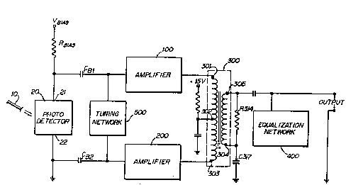
Fig 4. shows a simplified block diagram of a broP~h~n~
optical receiver in accord~nce with the present invention.
An optical fiber 10 carries an amplitude modulated optical
signal to A photodetector 20. This photodetector may, for
WV ~ J~'l/U~YI~lJO9~g
- example, be a photodiode which is appropriately biased ~y
DC bias voltage (''V8,,Js'') applied through an appropriate
biasing network comprising resistors R~j~s1 and RB;-52 to produce
a DC current b~tween terminals 21 and 22 of the photodetector
5 when the photodetector is excited by the optical input signal.
The DC current between terminals 21 and 22 includes an AC
component which corresponds to the AC ~ignal modulating the
optical signal. It is typical that this AC component will
range between 50NHz and 550MHz or higher. The AC component
10 is separated from the DC signal by bloc~ing capacitors CB1 and
CB2 and ~mplified by ~mplifier stages 100 and 200. The o~L~uLs
of the amplifiers 100 and 200 are ronnected to terminals 301
and 303 respectively of transformer 300 which may be a ferrite
core transformer of the type commonly used in bro~dh~A r.f.
15 applications. The primary wi~Ai~ of the transformer 300 is
center tapped at a terminal 302 ~nd this terminal 302 is
connected through a capacitor to ground which at the
frequencies in question effectively co~cts the center tap
to y~oun~. The ~econ~A~y winAintJ of the ouL~IL transformer
20 300 may have a 75 ohm resistor co~cted across it in order
to facilitate a better match between the transformer ouL~u~
~nd the 75 ohm system imre~se for further distribution of
the RF signals in a CATV network.
Optionally, a frequency re~pQns~ egualization network 400
25 may be employed at the ohLyuL of the transformer 300 to help
flatten out any nonlinearities in the freguency response due
to imperfections in the circuitry. Amplifiers 100 and 200 may
be any type of amplifier suitable to amplifying the o~L~^uL of
a photodiode such as a high impeA~ce amplifier or
30 transimpe~a~re amplifier. Preferably, hl~w_ver, as ~et forth
below in the description of the presently preferred
embodiment, amplifier~ 100 ~nd 200 ~re of the transimpedance
type. Another optional feature of the present invention is
a t~n; ng network 500 co~nected between the input~ to the
35 amplifiers 100 and 200. As~ sed in greater detail below,
this t~ g network ~00 serves to peak the frequency ~cO~onse
of the entire circuit about the geometric mean of the center
of the desired band of operation.
Fig. 5 is a æchematic diagram of a ~t ~ ently preferred
40 but nevertheless merely illustrative embodiment of the
invention. Referr~ng to Fig. 5 a photodetector 20 which is
preferably a photodiode, receives an optical input æignal
transmitted to it by an optical fiber 10. The cathode
terminal 211 of the photodiode is co~ne~ted through a resistor
9 ~0~06~0
Rl to ground. The anode terminal 213 of the photodiode is
connected through a resistor R2 to a DC voltage which in the
preferred embodiment is ~15 volts. Terminal 211 of the
photodiode feeds a first transimpedance amplifier 100 through
5 a DC blocking capacitor C101. DC blocki~g capacitor C101 is
a .01 microfarad ceramic capacitor, as are all of the other
capacitors shown in Fig. 5 unless otherwise noted. The other
terminal 213 of the photodiode feeds a second transimpeA~n~
amplifier 200 through a DC blocking capacitor 201. Both of
10 these transimpedance ~mplifiers lO0 and 200 are configured
identically, and the following description of the
transimre~A~ce ~mplifier 100 ~lso applies to the
transimr~nce amplifier 200. In this regard it will be noted
that the tens and units digits of the identification number
15 of each component in amplifier 100 are identical to the tens
and units digits of the identification nll~hers in
correspon~in~ ~omronents of the amplifier 200.
The transimp~AAce amplifier loo is built round a field
effect transistor Q120, the source ("S") termi~Als of which
20 are connected to ground. A feedback path is provided between
the drain ("D~') terminal of the field effect transistor Q120
by a feedback resistor R121. The fee~hA~k resistor R121 is
a discreet component which is selected in accordance with the
application into which the amplifier is to be placed. For
25 example, if the optical fiber 10 fee~ing the photodiode 20 is
relatively long and the intensity of the lig~t fed to the
photodiode 20 is relatively low, corresro~ingly small
currents will be produced by the photodiode 20. It is
desireable that the o~L~hL voltage of the opticæl receiver be
30 in~r~n~Dnt of the intensity of the light fed to the
photodetector 20. Since a Qmall current flowing through a
large imre~ e can produce the ~ame voltage as a large
current flowing a small imre~-~c~, it is desireable for the
respective transimpeA~n~Qs of the transim~eA~c~ amplifiers
35 100 and 200 to be relatively high when these amplifiers are
used to amplify signals carried by relatively ~mall input
currents. A receiver which will be driven by relatively high
input currents should incorporate transimpe~ce amplifiers
with corresponAi~gly lower transim~e~An~ec. The
40 transimr~n~ of the transimre~nce amplifier ~tage
comprising the field effect transistor Ql20 and the feedback
resistor R121 is approximateiy equal to R121+V~l+Vc where VGt
(the Yoltage gain of stage 1) is equal to G~Z parallel and Z
parallel is equal to ~d of the GaAsFET in parallel with R121
~091i~2658 PCT/US91iO0929
20~0~iX0 lO
and the loss component of Ll08 (which is nominally 600 ohm
resistive in the frequency range of interest here. The output
capacitance of Q120 is relatively small and considered to be
insignificant. Thus, the transimpedance of the transimpedance
5 amplifier stage may be varied by selecting the value of the
feedback resistor R121. lt will be noted that in commercially
available transimpedance amplifiers packaged in integrated
circuits, such selection of a feedback resistor is not easily
accomplished by the end user. Where variable feedback
10 impedances have been used the range of transimre~Ances
available have not been great enough to compensate for the
range of light intensity values to the photodetector which may
occur in a CATV system using fiber optic transmission of video
signals. Moreover, nonlinearites inherent in such variable
15 feedback imre~nces can constitute a serious problem in the
present application. Thus, the discreet and highly linear
nature of the feedback resistors used in the present design
offer the advantage of allowing the amplifier to be
specifically adapted for an extremely broad range of varying
20 conditions of input signals.
In accordance with the above, when weak optical signals
are applied to the photodetector 20 the feedback resistor R121
may be selected to be in the range of approximately l,000 ohms
to 2 kilohms. Where S~LO~Y input signals to the photodetector
25 20 are expected the feedback resistor Rl21 may be selected to
be in the 200-1,000 ohm range. For extremely narrow band
transmissions (e.~., transmi~sion of only one TV ~Annel) or
for receiving a low intensity optical signal from an extremely
long fiber optic path, feedback resi~tors of over 2 kilohms
30 may be selected. Such resi~tors would also be suitable for
narrowband data transmission applications.
The gate of the field effect transistor Q121 is ro~nected
to the incoming RF signal passing through blocking capacitor
ClOl. The DC voltage which is applied to the gate of the
35 field effect transi~tor Ql20 is effectively ~nLLolled by a
bias regulating circuit built around transistor QllO. The
base of transistor QllO is ~G~ cted to ground through a
resi~tor Rl7 and to the l15 volt power supply through
resistors ~16 and Rl5. Rl5, 16 and 17 are selected to provide
40 an input bias reference voltage to the b~se of tr nsistor QllO
of approximately +3 volts. The collector of transistor Qllo
is connected to yL~nd through a blocking capacitor C104 and
to a -15 volt DC supply through a resistor R103. The
collector of transistor QllO is al~o connected to the gate of
11 205068Q
. ;
_ field effect transistor Ql20 through an inductor~LlO5~. -The
emitter of QllO is connected to the l~l5 volt DC power ~rough
a resistor Rl07 and back to the drain of the field effect
transistor Ql2Q through an inductor Ll08 which is essentially
5 an open circuit to radio frequency signals. Paths to ground
from the emitter of transistor QllO are provided by a blocking
capacitor 106 and a Zener diode CR130 which is normally non-
conducting and functions to limit the source to drain voltage
of Ql20 during turn-off or during power interruptions. The
10 Ql20 is a gallium arsenide field effect transistor tGaAsFET)
with a maximum voltage rating of 5 volts.
In the above circuit the base to emitter voltage drop
across the transistor QllO is approximately .7 volts. Thus,
if the transistor is conducting, the voltage at the emitter
15 of transistor QlOl will be approximately ~3.7 volts.
In the above circuit, the inductor Ll08 functions to
behave as short circuit to DC signals and to behave as a pure
resistive component to AC signals at the radio frequencies in
question ( e. over 50MHz). Preferably, Ll08 will appear to
20 be a resistive impe~ce of approximately 600 to 700 ohms at
frequencies in the 50MHz to 550MHz range. The inductor Ll08
may be formed of five turns of #30 enamel wire wound on a
ferrite core.
The drain terminal of the field effect tr~nsistor Ql20
25 is connected to terminal 301 at the primary windiny of the
o~L~uL transformer 300 via a high impe~nce buffer ~mplifier
stage. This buffer amplifier stage includes a transistor Ql40
whose sources are conn?cted to y o~.~ through a resistor Rl31
and a resistor Rl33. A radio frequency path to ground is
30 provided from a point in the circuit between resistor Rl3l and
Rl33 by a blocki n~ capacitor Cl32. The drain of the
transistor Ql40 is conn~cted to the terminal 301 at the
primary windin~ of the o~L~L transformer 300 and the gate of
Ql40 is cQnnected to the drain terminal of the field effect
35 transistor Ql20.
Ql40 has the characteristic of an amplifier with a source
feedback resistance path which is high enough to minimize any
loading of the previous stage thus providing a buffer between
the input GaAsFE~ and the amplifier ~L~-L.
The output transformer 300 is a 4 to l imp~nc~ matching
transformer which $s operable in the 40MHz to lGHz range. An
example of a transformer which is suitable for use as the
transformer 300 is the Toko part No. 458DB-1013. The terminal
303 At the primary win~ing of the o~L~uL transformer is
~ r ~ l ~ U~
.
12 2~068~
con~Gted to the ouL~u~ of the other transimpedance amplifie
200. The center tap terminal 302 at the primary winding is
co~nected to the +15 volt power supply through resistors ~312
and R311 and t~ ground through a blocking capacitor C313. The
5 transformer 300 preferably has a 2 to 1 turns ratio or a 4 to
1 impe~nc~ ratio. The transformer 300 acts to transform the
unbalanced load impedance at its ~uL~hL terminals 305 and 304
to a balanced load for the drains of the transistors Q140 and
Q240. The circuitry ~o~n~cted to the center tap terminal 302
10 of the primary win~ of the transformer provides an AC hort
to ground ~t that point ~nd also drops the DC voltage to an
optimum operating level.
A resistor R314 may, optionally, be cQnnected across the
output terr;~ 305 and 304 of the ouLyu~ transformer 300 to
15 improve the impe~nce match (e.~., 75 ohms) to any st~Ard
CATV co~Y~l equipment (no shown) fed by the output
transformer 300. Bloc~in~ capacitor C317 provides a path from
terminal 304 to yLOU~d for r.f. ignals, and blocking
capacitor C310 provides a path for the radio frequency signal
20 to the ohLyh~ terminals of the receiver. The output of the
receiver may, optionally, be conn~ted to an equalization
network 400 comprising a resistor 401 rQ~nected in series to
a variable inductor L4 02 which in turn is co~n~cted through
a resonating capacitor C403 to y~O~d- In the preferred
25 embodiment of inductor L402 is of the slug-tuned type. The
equalization network 400 is utilized to correct for out any
nonlinearities in the responce of the receiver caused by
imperfections in the rem~; n~Pr of the circuitry.
Another feature of the receiver of the present invention
30 is that the gates of the field effect transi~tor~ Q120 and
Q220 are ~o~Pcted to each other ~y a tllnin~ network 500
comprising ~ ~-~p~c~tor C9 and variable inductor L3.
Preferably, inductor L3 i~ a ~lug-tuned inductor. The purpose
of the inductor L3 i8 to compensate for the capacitance of the
35 photoAio~e 20, the strAy cAp~c;tance of the inte~--Y l~cting
circuitry, and the input capacitance of the FET's Q120 and
Q220. L3 is adjusted 80 that a frequency response will be
obtA;~e~ which peaks at the geometric mean of the center of
the band of operation. In the preferred embodiment
40 illustrated, the amplifier has a ~ :p r~-? ranging from S0 to
550MHz. The inductor L3 i8 thus adjusted to obtain a broad
peak in reayl- -- at 166MHz. It should be noted that the
v~riable inductor L3 provides means for shifting the useful
band of oper~tion of the ~mplifier for special applications.
13 ~050~8a
The circuit illustrated by Fig. 5 operates in the
following manner. Optical energy is transmitted to the
photodiode detector 20 via the optical fiber 10. The
photodiode 20 is reversed biased by the biasing network
comprising resistors R2 and Rl. This reverse bias ensures
that the photo diode 20 operates in its most linear region
(i.e., in the region between point A and point B of Fig.
3). In the presence of light from the optical fiber 10 the
current flowing through the photodiode 20 is determined by
the responsivity of the photodiode 20 and the incident
optical power applied to the input of the photodiode. This
current will typically range between approximately 50 and
1,000 microamperes. When there is r.f. modulation of the
amplitude of the light carried by fiber 10, the DC current
through the photodiode will also have r.f. amplitude
component corresponding to the degree of amplitude
modulation of the light from fiber 10. This r.f. component,
which comprises the carrier frequencies of the video
signals transmitted over the optical fiber 10, flows
through the low impedance radio frequency path provided by
blocking capacitors C101 and C201 and thereby to the gate
circuits of field effect transistors Q120 and Q220 of the
respective transimpedance amplifiers 100 and 200. As
indicated above, the feedback, resistors R121 and R221 of
the respective transimpedance amplifiers 100 and 200 are
selected to provide input impedances which are suitably
matched to the input signals to the transimpedance
amplifiers 100 and 200 produced by the photodiode 20. When
the fiber optic path 10 is long and the light intensity at
its output to photodiode 20 is low, thus resulting in
photodiode 20 providing a relatively low level input signal
to the transimpedance amplifier 100 and 200, relatively
high resistance values (e.g., in a range of l,000 to 2,000
ohms) are selected for the values of Rl21 and R221. For
applications in which relatively high input signals to the
transimpedance amplifiers are expected to be generated by
the photodetector 20, relatively low resistance values
X
205068~
.~
13a
(e.g., in the range of 200 to 1,000 ohms) are selected for
R121 and R221.
QllO and Q210 and their associated circuitry provide
bias regulation for the transimpedance amplifiers 100 and
200 respectively. They control the voltage which is
applied to the gates of the field effect transistors Q120
and Q220 and regulate the drain to source current flow.
For optimum linearity it is preferable to hold the drain
current flow to
r~l/ U~ U~Y
~$~80 14
a range of approximately 25 milliamps d.c. Referring to th
transimpedance amplifier 100, for example, this regulation of
current flow is accomplished in the following manner. The
transistor Q1~0 has an input reference voltage which is
5 derived from the +15 volt power supply by the resistor network
comprising resistors R15, R16 and R17. In the preferred
embodiment, this resistor network produces a voltage at the
base of transistor Q101 of approximately +3 volts. The
emitter to base voltage drop across transistor QllO is
10 approximately .7 volts. Thus, when transistor Q110 is
con~n~ting and the voltage ~t the resistor R107 and inductor
L108 is approximately 4 volts, L108 functions to minimize the
r.f. load admittance on the drain of Q120 thereby preserving
the available voltage gain of Q110. L108 also provides a low
15 d.c. resistance path for the drain current of Q120.
A zener diode CR130 co~ected, between the emitter of
Q110 and ground facilitates the process of applyin~ or
removing power from the circuitry illustrated in Fig. 5.
CR130 does not function during normal operation (i.e., it
20 appears to be an open circuit). While power is being turned
on or off, however, CR130 acts as a voltage limiter to prevent
the drain voltage of GaAsFET Q120 from excee~i~q the rated
voltage (5v. nominal). ~ree~;n~ the rated voltage could
cause damage to GaAsFET Q120.
The magnitudes of the respective r-~L~uL ~ignals of field
effect transistors Q120 and Q220 are determined by the input
currents applied to these transistor circuits multiplied by
the circuit transimpe~nce, which as explained above, follow
the value of the ~_~e~Live feedback resi~tors R121 and R221.
30 The r.f. voltage signals at the drains of transistors of Q120
and Q220 are fed ~-pcctively to the gate circuits of the high
i~pe~Ance buffer amplifiers formed by Q140 and Q240 and their
associated circuitry. The ouL~s of these buffer amplifiers
are applied to the prim~ry w;~ g of ou~ transformer 300.
The GuL~uL transformer 300 is set up in a bal~nced
configuration which is reguired for a push-pull ampl~fier
application. It serves to match the ~uL~uL of the buffer
amplifier stages to a conventional roAy;~l cable system for
further distribution to homes cQn~octed to the co~Yi~l cable
40 system.