Note: Descriptions are shown in the official language in which they were submitted.
2050731
SPECIFICATION
Title of the Invention
SUPERCONDUCTINTG DE~ICE HAVING A REDUCED
~HICKNESS OF OXIDE SUPERCONDUCTING LAYER
AND METHOD FOR MANUFACI'UR~NG THE SAME
Background of the Invention
Field of the invention
The present invention relates to a superconducting device and a
method for manufacturing the same, and more specifically to a
superconducting device including an oxide superconducting layer having a
planar upper surface and a partially reduced thickness, and a method for
manufacturing the same.
Description of related art
Typical three-terminal deYices which utilize a superconductor
include a so called superconducting~base transistor and a so called
super-FET (field effect transistor). The superconducting-base transistor
includes an emitter of a superconductor or a normal conductor, a tunnel
barrier of an insulator, a base of a superconductor, a semiconductor
isolator and a collector of a normal conductor, stacked in thc named
order. This superconducting-base transistor operates at a high speed and
wi~ a low power consumption, by utili~ing high speed electrons passing
through the tunnel barrier.
The super-FET includes a semiconductor layer, and a
superconductor source electrode and a superconductor drain electrode
2050~31
which are formed closely to each other on the semiconductor layer. A
portion of the semiconductor layer between the superconductor source
electrode and the superconductor drain electrode has a greatly recessed or
undercut rear surface so as to have a reduced thickness. In addition, a
gate electrode is formed through a gate insulator Jayer on the recessed or
undercut rear surface of the portion of the semiconductor layer between
the superconductor source electrode and the superconductor drain
electrode.
A superconducting current flowing through the semiconductor
layer portion between the superconductor source electrode and the
superconductor drain electrode due to a superconducting proximity effect
is controlled by an applied gate voltage. This super-FET also operates at
a high speed with a low power consumption.
In addition, in the prior art, there has been proposed a
three-terminal sllperconducting device having a channel of a
superconductor fo~ned between a source electrode and a drain electrode,
so that a current flowing through the superconducting channel is
controlled by a voltage applied to a gate formed aboYe the
superconducting channel.
Both of the above mentioned superconducting-base transistor and
the super-FET have a portion in which a semiconductor laycr and a
superconducting layer are stacked to each other. However, it is difficult
to form a stacked structure of the semiconductor layer and the
superconducting layer ~ormed of an oxide superconductor which has been
recently advanced in study. In addition, even if it is possible to form a
stacked structure of the semiconductor layer and the oxide
superconducting l~yer, it is difficult to control a boundary between the
20S0731
semiconductor layer and the oxide superconducting layer. Therefore, a
satisfactory operation could not been obtained in these superconducting
devices.
In addition, since the super-FET utilizes the superconducting
proximity effect, the superconductor source electrode and the
superconductor drain electrode have to be located close to each other at a
distance which is a few times the coherence length of the su~ercol~dl~ctQr
materials of the superconductor source electrode and the superconductor
drain electrode. In particular, since an oxide superconductor has a short
coherence length, if the superconductor source electrode and the
superconductor drain electrode are formed of the oxide superconductor
material, a distance between the superconductor source electrode and the
superconductor drain electrode has to be on the order of a few ten
nanometers. It is very difficult to conduct a ~lne processing such as a fine
pattem etching so as to ensure the Yery short separation distance. Bec~lse
of this, in the prior art, it has been impossible to manufacture the
super-FET composed of the oxide superconductor material.
Furthermore, it has been confirmed that the conventional
three-terminal superconducting device having the superconducting
channel shows a modulation operation. However, the conventional
three-terminal superconducting device having the superconducting
ch~nnel could not realize a complete ON/OFF operation, because a carrier
density is too high. In ~his connection, since an oxide superconductor
material has a low carrier density, it is expected to form a three-terminal
superconducting device which has a superconducting channel and which
can realize the complete ON/OFF operation, by forming the
superconducting channel of the oxide superconductor material. In this
- 3 -
205073~
connection, however, a thickness of the superconducting ch~nnel has to be
made on the order of five nanometers.
On the other hand, typical two-terminal devices which utilize a
superconductor include a so ca~led Josephson device, which con~l;ses a
pair of superconductors coupled to each other through a tunnel barrier.
The Josephson device can rea~ize a high speed swi~hing.
Thc Josephson device formed of an oxide superco~d~lctor material
thin ~llm can be realized in the form of a planer type, which is divided
into a Dayem bridge (DMB) type and a variable thickness bridge (VTB)
type.
The Dayem bridge type ~osephson device has been folmed of a
constant thickness oxide superconductor thin film which is formed on a
substrate and which is patterned in a plan view, so dlat a supercol.ductor
thin film region having a greatly narrow width is formed between a pair
of superconductor thin film regions having a sufficient width. In other
words, the pair of superconductor thin film regions having a sufficient
width are coupled to each other by the superconductor thin film region
having the greatly narrow width. Namely, a weak link of the Josephson
junction in the superconductor thin ~llm is folmed at the greatly narrow
width region.
On the other hand, the variab]e thickness bridge type Josephson
device has ~een formed of an oxide superconductor thin film of a
sufficient ~ickness which is fonned on a substrate and which is partially
etched or thinned in a thickness direction, so that a thinned oxide
superconductor thin film portion is formed between a pair of
superconductor thin film portions having the sufficient dlickness. In
other words, the pair of superconductor thin film portions having the
2050731
sufficient thickness are coupled to each other by the thinned oxide
superconductor thin film portion. Accordingly, a weak link of ~e
Josephson junction is fonned at the reduced thickness portion of the oxide
superconductor thin film.
As would be understood from the above, a characteristics of the
planar type Josephson device has a close relation to the width of the
superconductor thin filn~ region having the greatly narrow width in the
Dayem bridge type Josephson dev~ce, and to the thickness of ~e ~ ".e~
oxide superconductor thin film portion in the variable thickness bridge
type Josephson device, both of which form the weak link of the Josephson
junction. Therefore, in order to obtain a desired characteristics with a
good repeatability, a high precision on a sub-micron level of the
processing such as the etching is required.
The Dayem bridge type Josephson device can be said to be more
preferable than the variable thickness bridge type Josephson device, since
the Dayem bridge type Josephson device has a relatively planer surface,
which is preferred in a integrated circuit. However, in order to form the
weak link in the Dayem bridge type Josephson device, it is required to
pattern an oxide superconductor thin film having the thickness on the
order of 0.5~1m to 1.0,um into a width of not greater than 0.2~m.
However, it is very difficult to ~onduct this fine patterning with good
repeatability.
On the other hand, in the variable thickness bridge type Josephson
device, the very fine pattering is not required in order to form the weak
link. However, it is very difficult to uniformly control the rem~ining
thickness of the thinned portion forming the weak link. In addition, the
variable thickness bridge type Josephson device cannot have a
20~0731
satisfactorily planer surface. This is not preferable to the integrated
circuit application.
Sumrnary of the Invention
Accordingly, it is an object of the present invention to provide a
superconducting device and a method for manufacturing the same, which
addresses the above mentioned defects of the conventional ones.
Another object of the present invention is to provide an FET type
superconducting device including an channel composed of an oxide
superconducting layer having a planar upper surface and a partially
reduced thickness, and a method for manufacturing the same with a good
repeatability by using existing established processing techniques.
Still another object of the present invention is to provide a
Josephson junction superconducting device including a weak link
composed of an oxide superconducting layer having a planar upper
surface and a partially reduced thickness, and a method for manufacturing
the same with a good repeatability by using existing established processing
techniques.
In accordance with one aspect of the invention there is provided a
superconducting Josephson device comprising a substrate having an
insulating projection formed on a principal surface and an oxide
superconductor thin film covering the projection formed on said principal
surface and having a substantially planar surface. The oxide superconductor
thin film has a thin portion on the projection, a first thick portion at one
side of the projection and a second thick portion at the other side of the
- 2050731
projection, the thin portion of the oxide superconductor thin fiim
positioned on the projection of the substrate having a thickness of five
nanometers in order to form a Josephson weak link, so that a
superconducting current can flow between the first thick portion and the
second thick portion through the thin portion of the oxide superconductor
thin film.
A gate electrode can be formed through an insulation barrier on the
thinned portion of the oxide superconductor thin film positioned on the
projection of the substratet so that the electric current flowing between
the first and second electrodes through the thinned portion of the oxide
superconductor thin film is controlled by a voltage applied to the gate
electrode. In this case, the superconducting device constitutes a
super-FET, and one of the first and second electrodes forms a source
electrode and the other forms a drain electrode. In this connection, the
first and second electrodes and the gate electrodes can be formed of a
superconducting material, but can also be formed of a material, such as a
normal conducting material, other than the superconducting material.
As mentioned hereinbefore, in the conventional super-FET, a
superconducting current flows through the semiconductor channel due to
the superconducting proximity effect. However, in the super-FET in
accordance with the present invention, a main current flows through the
superconductor. Therefore, the limitation in the fine processing
techniques required for manufacturing the super-FET can be relaxed.
The invention also provides a method for manufacturing a
superconducting device, comprising the step of preparing a substrate having
a projection formed on a principal surface thereof, and forming an oxide
superconductor thin film on said principal surface of the substrate including
the projection. The substrate is prepared by selectively forming a resist at a
,~
~ .
20l~0731
projection forming position on the principal surface of the substrate and
etching the principal surface of the substrate using the resist as a mask so
that on the principal surface of the substrate there is formed a projection
having a width narrower than the resist mask by a side etching; the oxide
superconductor thin film as a thickness larger that the height of the
projection, and a whole of an upper surface of the oxide superconductor
thin film has a planar upper surface and therefore the thickness of the oxide
superconductor thin film on the projection, being of five nanometers is
thinner that the thickness of the oxide superconductor thin film on the
substrate other than the projection.
As mentioned hereinbefore, in the conventional superconducting
device, after the superconductor thin film having a uniform thickness and
flat upper and lower surfaces was formed, the superconductor thin film is
partially abraded or removed in a thickness direction so as to form a
thinned superconductor thin film portion which constitutes a
superconducting channel in the super-FET and a weak link in the
Josephson device. However, since the required thickness of the thinned
superconductor thin film portion is very small, an extremely high degree
of precision in a fine processing (for example, etching~ has been required
in order to obtain a desired characteristics of the superconducting device.
On the other hand, in the above mentioned method in accordance
with the present invention, since the superconductor thin film is formed to
cover the projection, and then, a whole surface of the superconductor thin
film is removed back and planarized. Therefore, it is no longer necessary
to conduct a high degree of fine processing such as a fine etching.
In addition, since the upper surface of the superconductor thin film
has a planarized upper surface, the superconducting device is very
convenient in order to be assembled in an integrated circuit.
~ .. ,
2()5~73`1
In the super-FET, the superconducting ch~nnel is turned on and off
by a voltage applied to the gate electrode. Therefore, a thickness of the
superconducting channel has to be on the order of five nanometers in ~e
direction of an electric field created by the voltage applied to the gate
electrode. This extremely thin superconducting ch~nnel can be easily
realized or formed in accordance with the method of the present
invention, since the superconducting channel is formed of the oxide
superconductor thin film portion which is positioned on the projection of
the substrate and which had been extremely thinned by removing and
planarizing the whole upper surface of the oxide superconductor thin film
foImed on the princip~l surface of the substrate having the proiection.
If the oxide superconductor thin film is simply deposited or grown
on the principal surface of the substrate having the projection, the
thickness of the oxide sllperconductor thin film on the projection is the
same as that of the oxide superconductor thin film on ~e principal surface
without the projection. As mentioned above, in the present in~ention, ~e
whole of the oxide superconductor thin film thus fo~ned is planarized so
as to thin the oxide superconductor thin film portion on the projection.
Since the whole of the oxide superconductor thin film can be easily
planarized and removed with a high degree of controllability, it is
possible to relatively easily form the oxide superconductor tbin film
having a desired thickness on the projection of the principal surface of the
substrate.
The superconducting device in accordance with the present
invention, the substrate, on which the oxide superconductor thin film is
deposited, can be formed of an insu~ating substrate, preferably an oxide
single crystalline substrate such as MgO, SrTiO3, CdNdAl04, etc. These
2050731
substrate materia]s are very effective in forming or growing a crystalline
film having a high orientation property. Howe~er, the substrate can be
formed on a semiconductor substrate if an appropriate buffer layer is
deposited thereon.
Fu.ll~e.ll~ore, the oxide superconductor thin ~llrn can be fo~med of
different oxide superconductor materials, for example, a Y-Ba-CN O type
compound oxide superconductor material, a Bi-Sr-Ca-Cu-O type
compound oxide superconductor material, and a Tl-Ba-Ca-Cu-O type
compound oxide superconductor material.
The above and other objects, features and advarltages of the ~l~SC.It
invention will be apparent from the following description of preferred
embodiments of the invention with reference to the accompanying
drawings.
Brief Description of the Drawings
Figure 1 is a diagran~m~tic sectional view of one embo~ nt of the
superconducting device in accordance with the present invention;
Figures 2A to 2H are diagrammatic sectional views for illustrating
the process for manufacturing the superconducting device shown in
Figure l;
Figure 3 is a diagrammatic perspective view of anodler embodiment
of the superconducting dev~ce in accordance with the present invention;
and
Figures 4A to 4H are dia~rarnmatic sectional views for illustrating
the process for manufacturing the superconducting device shown in
Figure 3.
- 10-
2050731
Description of the Preferred embodiments
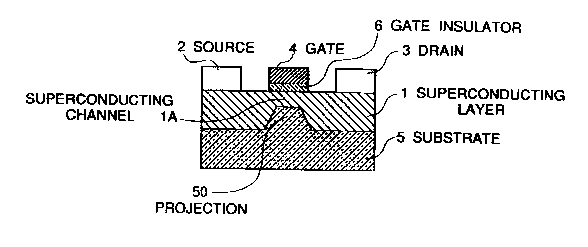
Referring to Figure 1, there is shown a diagr~mn~tic sectio~l view
of one embodiment of the superconducting device in accordance wi~ the
present invention. The shown superconducting device is a super-FET.
The super-FET includes an oxide superconducting layer 1 forrned
on a principal surface of a substrate 5 having a projection 50. -The oxide
superconducting layer 1 has a planarized upper surface, and th~r~fol~, a
portion of the oxide sllperconducting layer 1 on-the projection is thinner
than the other portion of the oxide superconducting layer 1. This thin
portion of the oxide superconducting layer 1 on the projection folms a
superconducting channel lA. On the superconducting ch~nnel lA, a gate
electrode 4 is formed through a gate insul~tor 6. In additlon, a source
electrode 2 and a drain electrode 3 are formed on the oxide
superconducting layer 1 at both sides of the superconducting ch~el lA,
Now, the process for manufacturing the above mentioned
superconducting device will be descri~ed with reference to Figures 2A to
2H.
First, the substrate 5 is prepared as shown in Figure 2A. This
substrate 5 is formed of for example, an insulating substrate such as a
MgO (100) substrate, a SrTiO3 ~100) substrate or others, or a
semiconductor substrate such as a silicon substrate having a principal
surface coated with an insulating film. However, if the semiconductor
substrate is used, after the projection is formed on the principal surface,
the insulating film is formed on the principal surface.
As shown in Figure 2B, a photoresist mask 8 is fo~ned on a portion
of the principal surface of the substrate S corresponding to a projection
fom~ing position, and the principal surface of the substrate S is selectively
20~0731
etched or recessed by a dry etching process such as an Ar ion etching, so
that a projection 50 is formed on the principal surface of ~e substrate 5.
Thereafter, the photoresist mask 8 is removed.
In the case that a semiconductor substrate is used, a crystalline
direction is important, and therefore, the process is modified. Por
example, if a silicon substrate is used, a photoresist mask 8 is forme~ so as
to ensure that a gate length direction (a channel current direction) is in
parallel to a Si(100) plane and perpendicular to a Si(llO) plane. The
silicon substrate partially masked with the photoresist 8 is etchPd with an
etching liquid such as KOH or APW, so that a projection 50 is formed.
After ~e photoresist mask 8 is removed, the principal surface having the
projection 50 is continuously coated with MgA104 by a CVD (chemical
vapor deposition) and with BaTiO3 by a sputtering process.
Then, as shown in Figure 2C, an oxide superconductor thin fi~n 1
is deposited on the pnncipal surface of the substrate 5, by for exPrnple an
off-axis sputtering, a reactive evaporation, an MBE (molecular beam
epitaxy), a CVD, etc. Tbe oxide superconductor material is prefe~ably
formed of, for example, a Y-Ba-Cu-O type compound oxide
superconductor material, a Bi-Sr-Ca-Cu-O type compound oxide
superconductor material, and a TI-Ba-Ca-Cu-O type compound oxide
superconductor material. In addition, a c-axis orientated thin film is
preferably deposited, since the c-axis orientated thin film has a large
critical current density in a direction in parallel to the substrate sllrface.
The oxide superconductor thin film 1 as deposited has a unifolm
thickness anywhere. Therefore, it is necessary to planarize an upper
surface of the deposited oxide superconductor thin film, and to thin an
o~ide superconductor thin film portion on the projection 50. For ~is
- 12-
2050731
purpose, as shown in Figure SD, a photoresist layer 9 is deposite~l on the
oxide superconductor thin film 1 in such a m~nner that the deposited
photoresist layer 9 has a plat upper surface.
Thereafter, as shown in Figu~ 2E, an Ar ion etching is perfonned
until the upper surface of the oxide superconductor thin film 1 is
planarized and a thickness of the oxide superconductor thin film 1 on ~e
projection 50 becomes five nanometers so as to constitute the
sllperc~.lducting channel ] A
Next~ a gate electrode is formed on the superconducting channel
lA. This gate electrode is preferably composed of an insulating layer
formed on the superconducting channel lA and a metal layer stacked on
the insulating layer. For this purpose, as shown in Figure 2F, an
ins~ in.~ layer 6A and a metal layer 7 are sequentially forrned on the
oxide superconductor thin film 1. The insulating layer 6A is forrned of
an insul~tjng material such as MgO, which does not form a large density
of energy levels between the superconductor ~in ~llm 1 and the inc~ ing
layer 6A. On the other hand, the metal layer 7 is preferably formed of a
refractory metal such as Ti, W, etc., or Au, or a silicide thereof.
The stacked layer of the insulating layer 6A and the metal layer 7 is
selectively removed by etching, so th~t ~he gate electrode 4 is formed on
only the superconducting channel lA, as shown in Figure 2G.
Finally, as shown in Figure 2H, a source electrode 2 and a drain
electrode 3 of Au are formed on the oxide superconductor thin ~llm 1 at
both sides of the gate e~ectrode 4, respectively. With this, the super-FET
in accordance with the present invention is completed.
As explained above, if the super-FET in accordance with ~he
present invention is manufactured in accordance with the method of dle
20~0731
present invention, the limitation in the fine processing techni~ue required
for manufacturing the super-FET is relaxed. In addition, since ~e upper
surface of the superconductor thin film is planarized, it become easy to
form conductor wirings in a later process. Accordingly, it is easy to
manufacture the super-FET with good repeatability, and dle manufactured
super-PET has a stable perfoImance.
Referring to Figure 3, there is shown a diagr~rnrn~tic ~pc~ti~e
view of another embodiment of the superconducting deYice in accordance
with the present invention. This second embodiment is a Josephson
device.
The Josephson device includes a substrate 10 and an oxide
superconductor thin filrn 20 formed on the substrate 10. The substrate 10
includes a projection 10A formed on a principal surface thereof. On the
other hand, the oxide superconductor thin film 20 forrned on the substrate
10 has a planarized upper surfacet and therefore, has a reduced thickness
on the projection l0A.
The reduced thickness portion of the oxide superconductor thin film
20 on the projection 10A forms a weak link 20A of ~e Josephson device.
Oxide superconductor thin film portions at both sides of the weak link
20A fo~n a pair of superconductor electrode regions 20B and 20C,
respectively. Thus, the weak link 20A and the superconductor electrode
regions 20B and 20C are formed of a single oxide superconductor thin
film integrally deposited on the substrate. In addition, a pair of n~nnal
conductor electrodes 30A and 30B can be formed on the superconductor
electrode regions 20B and 20C, respectively.
Now, the process for manufacturing the above mentioned
superconducting device will be described with reference to Figures 4A to
- 14 -
20~073~
4H In the embodiment which will be described below, a Y-Ba-Cu-O type
compound oxide superconductor material is used for foIming ~e oxide
superconductor thin film.
First, the substrate lO having a flat upper or principal surface is
prepared as shown in Figure 4A. This substrate 10 is formed of a silicon
substrate wafer. As mentioned hereinbefore, however, ~e substrate can
be fo~ned of an insulating substrate such as a MgO (100) substrate, a
CdNdAl03 (001 ) substrate or others. - If ~hese substrates are used, a c-axis
orientated oxide superconductor thin film having a large critical current
density in a direction in parallel to the substrate surface can be formed on
the substrate.
As shown in Figure 4B, a photoresist layer 12 is formed to cover
the whole of the principal surface of the substrate lO. As shown in Figure
4C, the photoresist layer 12 is patterned so as to forrn or leave on the
principal surface of the substrate lO a photoresist mask 14 which is
slightly larger in a plan view size than that of a cul-e.ll direction length of
the weak link region 20A of a final or completed Josephson device. Ln
this case, the photoresist mask 14 is forrned so as to ensure that a
lengthwise direction of the photoresist mask 14 (a direction pe~pendicular
to the paper surface of Figure 4C~ is in parallel to a (llO) plane of the
silicon substrate 10.
Therefore, as shown in Figure 4D, the principal surface of the
substrate 10 partially masked with the photoresis~ mask 14 is wet-etched
with an etching liquid such as KOH or APW, so that a projection lOA is
fonned on dle principal surface of the substrate. In this etching process,
by promoting a side etching, it is possible to form the projection lOA
having a width shorter than the photoresist mask 14 in the current
20~0731
direction length of the weak link region 20A of the final or completed
Josephson device.
As mentioned above, since the substrate 10 is formed of the silicon
wafer, it is necessary to form a buffer layer on the substrate 10 befor~ the
oxide superconductor thin film is deposited on the substrate 10. For this
purpose, after the photoresist mask 14 is remove~, the prin~ipal surface
having the projection lOA is continuously coated with MgAl04 by a CVD
and with BaTiO3 by a sputtering process, so that a buffer layer 16 is
formed on the principal surface of the substrate 10.
Then, as shown in Figure 4F, an oxide superconductor thin film 20
is deposited on the buffer layer 16. The deposited oxide superconductor
thin ~llm 20 has to have a thickness larger than a height of ~e projection
lOA. The oxide superconductor thin film 20 can be deposited, by for
example an off-axis sputtering, a reactive evaporation, a CVD, etc. In
this example, the off-axis sputtering is performed under the condition that
a sputtering gas is composed of Ar and 02 at the rate of Ar: 02 = 9: 1,
the sputtering gas pressure is 10 Pa, and the temperature is 7~0'C.
The oxide superconductor thin film 20 as deposited has a unifonn
thickness anywhere, and therefore, has a projection corresponding to the
projection 10A of the substrate 10. Therefore, it is necessary to planarize
an upper surface of the deposited oxide superconductor thin film and to
thin a oxide superconductor thin film portion on the projection lOA. For
this pu~pose, as shown in Figure 4G, a photoresis~ layer 22 is deposited on
the o~ide superconductor thin ~llm 20 in such a manner that the deposited
photoresist layer 22 has a plat upper surface.
Thereafter, as shown in Figure 4H, a reactive ion etching or
another etching process is performed so that the photoresist layer 22 and
- 16-
20~731
the oxide superconductor thin film 20 are etched back and the upper
surface of the oxide superconductor thin film 20 is planarized.
With this planarization of the oxide superconductor thin ~llm 20,
the thickness of the oxide superconductor thin fi]m 20 on the projection
10A becomes thinner than that of the oxide superconductor thin film 20
on the other portion of the oxide superconductor thin film 20. Therefore,
~e etch-back process is controlled so as to ensure that the thinnlGr portion
20A of the oxide superconductor thin film 20 on the projection lOA has a
thickness capable of forming a weak link of the Josephson device.
Specifically, the thickness of the thinner portion ~OA is controlled to be
on the order of five nanometers to 10 nan~meters.
The invention has thus been shown and described with ~ef~ ce to
the specific embodiments. However, it should be noted that thc present
invention is in no way limited to the details of the illustrated structures
but changes and modifications may be made within the scope of the
appended claims.