Note: Descriptions are shown in the official language in which they were submitted.
1 2051030
SEMICONDUCTOR POWER CONVERSION SYSTEM
HAVING A MULTIPHASE BRIDGE CIRCUIT
The present invention relates to a semiconductor power conversion
system which is used for AC-to-DC conversion, DC power transmission,
frequency conversion, etc. in the fields of electric power systems, electric
railways, large-scaled plants, etc. More particularly, it relates to a
semiconductor power conversion system which is well suited for, e.g., a
variable speed generator/motor that needs to continue running perfectly even
in a case where an AC input voltage has fluctuated due to an abnormali~y of
the electric power system or a case where the load of a DC output side is an
inductive circuit, so an overvoltage develops due to a current source
operation.
Conventional semiconductor power conversion systems will be discussed
hereinbelow in conjunction with the drawings.
BRIEF DESCRIPTION OF THE DRAWINGS
Fig. 1 is a circuit diagram showing the construction of the first
embodiment of the present invention;
Fig. 2 is a block diagram showing an example of a protection
interlocking device which is well suited to the embodiment;
Fig. 3 is a block diagram showing an example of a protection
interlocking device which is well suited to the construction of the second
embodiment of the present invention;
r_ ~
2051030
Fig. 4 is a w~vero~ diagram showing the operation of the first
embodiment;
Fig. S is a circuit diagram showing the construction of the third
embodiment of the present invention;
S Fig. 6 is a block diagram showing an example of a protection
interlocking device which is well suited to the construction of the third
embodiment of the present invention;
Fig. 7 is a block diagram showing an example of a protection
interlocking device which is well suited to the construction of the fourth
embodiment of the present invention;
Fig. 8 is a circuit diagram showing the construction of the fifth
embodiment of the present invention;
Fig. 9 is a block diagram showing an example of a protection
interlocking de-vice which is well suited to the construction of the fifth
embodiment of the present invention;
Fig. 10 is a circuit diagram showing the construction of a semiconductor
power conversion apparatus in the prior art;
Fig. 11 is a circuit diagram showing an example of an input current
detecting circuit which can be used in the present invention;
Fig. 12 is a flow chart showing the processing flow of a protective
operation in the prior art semiconductor power conversion apparatus; and
Figs. 13 through 17 are diagrams for explaining the operation of the
present invention.
A
20511)30
In a case where a conventional semiconductor power collvel~ion
apparatus of the line co~ ulation type is applied to equipment with the
intention of enh~ncing the stability of an electric power system, there is a
problem as stated below:
Since the thermal capacities of semiconductor devices for electric power,
such as thyristors, are smaller than those of transformers, rotary electric
machines, etc., the protective operation in the event of any abnormality
accruing is inevitably designed to be highly sensitive. With the semiconductor
power conversion apparatus, therefore, the operation thereof must sometimes
10 be interrupted in consideration of the protection of the power semiconductor
devices even when the disturbance of the electric power system side is slight.
Herein, once the operation of the apparatus of this type has been interrupted,
it cannot be restarted until various items are inspected and confirmed tO be
secure and safe. Accordingly, the time period for the interruption becomes
15 long, and the apparatus cannot satisfactorily contribute to the enhancement of
the stability of the electric power system.
A prior art apparatus for solving such a problem is disclosed in the
official gazette of Japanese Patent Application Laid-Open No. 52699/1988.
Fig. 10 is a connection diagram showing the circuit arrangement of the
20 prior art example. The illustrated semiconductor power conversion apparatus
is so constructed that electric power is fed from an AC system 1 to a three-
phase bridge circuit 3 through a power transrolmer 2.
.~
,
4 2051030
Referring to the figure, the apparatus includes ~;ullellt transformers S for
detecting three-phase AC input cullellt values, a DC current transformer 6
for detecting a DC side output ~;ullellt value, and an input cullellt detector
circuit 7.
S Besides, it includes a subtractor 6a for finding the dir~elellce between
the output Iac of the input current detecting circuit 7 and the output Idc of
the DC current transformer 6, an absolute value calculating circuit 8 for
finding the absolute value of the output of the subtractor 6a, a differential
current detector 9, an overcurrent detector 10, and an operation continuation
deciding unit 11.
The output Iac of the input current detecting circuit 7 representing an
input current value and the output cullellt value Idc from the DC ~;ullent
transformer 6 are equal during the steady operation of the conversion
apparatus. A signal ~I obtained by rectifying the difference of both the
current values by means of the absolute value calculating circuit 8, is applied
to the differential current detector 9, while the input current value Iac is
applied to the o~/er~;ullent detector 10.
The operation continuation deciding unit 11 has logic functions as
indicated in detail in Fig. 12.
Referring to Fig. 12, if the output signal OC of the over-;ull~ nt detector
10 is "0" (step 100), the output current of the three-phase bridge circuit 3 is
decided to be normal (step 104), and an operation continuation command
G01 is output (step 107) so as to continue the steady operation.
2G510~0
How~vel, even when the output signal OC of the over-;ullellt detector
10 is "0", processing for a return to the normal operation of the collv~l~ion
apparatus (step 109) is required in the case where the normal operation is to
be restarted after the return of the apparatus from the output of a
5 suppression control command G02. To this end, it must be decided whether
or not the over~;ullellt suppression control command G02 was recently
delivered (step 108). Subject to the delivery of the command G02, the return
processing (step 109) is executed, and the operation continuation command
G01 is thereafter output (step 107).
Here, the contents of the return processing (step 109) are as follows:
i) In the state of the conversion apparatus before the detection of the
over~;ullellt, some of the calculated results of a control unit (not shown) for
controlling the gates of the individual thyristors of the three-phase bridge
circuit 3 are initialized on the basis of circuit currents at present. ii) The
15 present firing conditions of forward and backward thyristors TYS are taught
to the control unit, and these thyristors are initialized.
On the other hand, if the output signal OC of the ovel-;ullel~t detector
10 is "1" (step 100), the value of the output signal ~I of the absolute value
calculating circuit 8 is further decided (step 101). If the signal l~I is below an
20 allowable value K1 and nothing is wrong with a generator, then the
ove~ llent is decided to be ascribable to a power system fault or an
2051030
interrupter operation in another power conversion apparatus (steps 110, 103),
and the ~ver~;ullent suppression control command G02 is output to the
control unit (step 106).
The thyristor short-~;ir~;ui~ g switch TYS4 is fired in compliance with
S the over~;ullellt suppression control command G02, thereby suppressing the
~;ullent of the three-phase bridge circuit 3. Incidentally, the output of
the suppression control cornmand G02 is recorded by a flip-flop circuit
(not shown) or the like in order to prepare for the processing required when
returning to the normal operation (step 109).
Besides, in a case where the value of the output signal ~I of the
absolute value calc~ ting circuit 8 is equal to or above the allowable value
K1 (step 101), the overcurrent is decided to be ascribable to an internal fault
of the three-phase bridge circuit 3 (step 102), and an operation emergency
stop cornmand ST is output (step 105).
The firing signals of the thyristors TY1- TY6 of the three-phase bridge
circuit 3 are forcibly blocked in compliance with the operation emergency
stop command ST.
Here, even in case of an internal fault in another piece of equipment,
the signal ~I might fall below the allowable value K1. Therefore, whether
20 such an internal fault is pertinent is decided upon after the decision of the
step 101 (step 110). In the presence of the internal fault of the other
~5 1D~
equipment (step 111), the operation emergency stop co~",ua~d ST is output
in the same manner as in the case of the internal fault of the power
conversion apparatus (step 105) without carrying out the ~vell;ullent
sul~pres~ion control.
With the prior art technique, in detecting the abnormality of the power
conversion apparatus, the distinction is not s~ti~f~ctorily made between an
abnormality ascribable to the fault or damage in any equipment and an
abnormality, such as co~u~ation failure or overvoltage, caused under the
influence of a i~uctuation on the AC system side or the DC side. Even in the
abnormality of the colLImu~ation failure ascribable to the external fluctuation,for example, the conversion apparatus is subjected to an emergency stop
when the overcurrent signal OC has become "1" with the signal ~I reaching
the allowable value K1. This has led to the problem that the operating
reliability of the conversion apparatus cannot be ensured.
The first object of the present invention is to provide a semiconductor
power conversion system which is easy to restart even in the case where the
operation of a multiphase bridge carmot be continued due to a commutation
failure ascribable to an external fluctuation.
Besides, the second object of the present invention is to provide a
semiconductor power conversion system which is easy to restart even in a
case where the operation of a multiphase bridge cannot be continued due to
an overvoltage developed on a DC output side by an external fluctuation.
A
8 2~51030
In order to accomplish the first object, according to one aspect of the
present invention, there is provided a semiconductor power collvel~ion system
characterized by comprising: a multiphase bridge circuit which includes
semiconductor devices having a controllable firing function and a reverse
S blocking characteristic, a gate control circuit which gives firing commands to
said semiconductor devices, a short-cil~uiling switch in which switching
devices having a controllable firing function and a reverse blocking
characteristic are connected in a reverse parallel relationship to each other
and are connected in parallel with a DC output side of said multiphase bridge
10 circuit, and protection control means for pelrol~ing a control for protecting
said multiphase bridge circuit; said protection control means including: means
for detecting a co~ulation failure of said multiphase bridge circuit; and
means for operating upon the detection of the co~ ulation failure, to
produce a blocking command for blocking the firing of said semiconductor
15 devices of said multiphase bridge circuit and to produce a short-cil(;ui~illg
command for firing that one of said switching devices cbnsliLulillg said short-
circuiting switch which bypasses current of the comlllulation failure.
Besides, in order to accomplish the second object of the present
invention, according to another aspect thereof, there is provided a
20 semiconductor power conversion system characterized by comprising: a
multiphase bridge circuit which includes semiconductor devices having a
controllable firing function and a reverse blocking characteristic, a gate
,
205103~
control circuit which gives firing commands to said semiconductor devices, a
short~ ;ui~hlg switch in which switching devices having a controllable firing
function and a reverse blocking characteristic are connected in a reverse
parallel relationship to each other and are connected in parallel with a DC
S output side of said multiphase bridge circuit, and protection control means for
pel~,~ing a control for protecting said multiphase bridge circuit; said
protection control means including means for detecting an overvoltage on the
DC side of said multiphase bridge circuit, and means for operating upon the
detection of the overvoltage, to produce a blocking command for blocking the
10 firing of said semiconductor devices of said multiphase bridge circuit and to
produce a short-cilcuilillg command for firing that one of said switching
devices constituting said short-cil.;uiLillg switch in which the overvoltage forms
a forward voltage.
In each of the above aspects, said protection control means can further
15 include means for detecting a short-circuit release based on an expiration of
~;ullellt conduction of said short-~ ;uilillg switch and for halting the blocking
of the firing of said semiconductor devices of said multiphase bridge circuit.
Besides, in each of the aspects, said protection control means can further
include means for detecting a fault within said system (an internal fault)
20 attributed to either of said multiphase bridge circuit and a firing command
loop therefor; and means for operating upon the detection of the internal
20~1030
fault, in order to produce a blocking cc)mm~nd for blocking the firing of said
semiconductor devices constituting said multiphase bridge circuit and to
produce a short-cil-;uiling command for firing those of said switching devices
constituting said short-cill;uilillg switch which are bidirectional.
S Next, the operation of the present invention will be described by taking
a power conversion system having a three-phase bridge circuit as an example.
In the three-phase bridge of the power conversion circuit, as shown in
Fig. 13, two of six arms are usually conducting current in the six combinations
of (TY1 and TY2), (TY2 and TY3), (TY3 and TY4), (TY4 and TY5),
(TYS and TY6) and (TY6 and TY1). In the case of Fig. 13, the current
is being conducted in the combination of the two arms (TY1 and TY2).
Fig. 14 illustrates the course of a col~",ulation from the TY1 to the TY3.
Among the malfunctions of the power conve,~ion circuit, the
phenomenon of a col~ uLation failure is caused by a voltage fall on the AC
side of the circuit or a transient current from the DC side thereof even when
no internal fault occurs in the circuit. Regarding such a co~ uLation failure
ascribable to external factors, the normal operation of the circuit can be
resumed theleLoLu when the external fluctuation has diminished.
Fig. 15 shows an operating example on the occasion of the col"",ulation
20 failure as stated above. In the illustrated example, before a co~ llulation
from the I~Y3 to the TY5 termin~tes, the TY6 is fired to initiate a
co~ uLation from the IY4 to the TY6.
- 11 2~510~0
At this time, Iu = -Il + If, Iv = Il-It-If, and Iw = It hold. In Fig. 15, the
col-~u~ation ~;ullell~ If at the lower stage a~ xi"~tes to the ~;Ullellt IQ,
but the co~ ulation cullellt It at the upper stage decreases to zero again
because the potential of the v-phase becomes higher than that of the w-phase.
5 Therefore, the AC side is opened, and all of the cullellls Iu, Iv and Iw
become zero.
As a result, a short-circuit composed of TY3 and TY6 is formed on the
DC side as shown in Fig. 16, so that a direct current Idc remains at Il and
does not become zero.
Since the current flows continuously through TY3 and TY6 coll~lilu~illg
the short-circuit, the semiconductor devices TY3 and TY6 might be destroyed
due to the temperature rise thereof.
In order to ~revellt this drawback, a firing command is given to only the
TSP having the same polarity as those of the TY1- TY6, in the TSP and
15 TSN con~Li~u~ g the short-cil~uiLillg switch in Fig. 17, whereby the short-
cil~;ui~ g current Il is bypassed to the short-~;h~;ui~illg switch side. Herein, the
bypass to the short-cil.;uiLing switch side is ensured by a design in which the
forward voltage drop of the thyristor on the short-ciu~;uilillg switch side
is smaller than a device folw~d voltage drop on the three-phase bridge side
20 (in the example of Fig. 17, the sum of the forward voltage drops of the TY3
and TY6). Moreover, the three-phase bridge circuit is reliably opened by
forcibly blocking the firing command for the TY1 - TY6 as soon as the firing
command is given to the short-cil~;uiLillg switch.
2051~3~
When the current n on the DC circuit side has become zero in
accordance with the external fluctuation, the opening of the short-~;Lrcuilillg
switch is detected, and a forcible blocking command having been given to the
three-phase bridge is released, thereby enabling the re~uLu~lion of the steady
5 operation.
According to the above series of operations, when the three-phase
bridge is to be fired again, a short-circuit is not formed between it and the
short-circuiting switch, and the steady operation can be reliably resumed.
On the other hand, in the case of the internal fault, in order to stop the
10 three-phase bridge circuit quickly, the forcible blocking command is given to
turn off the TY1- TY6. Since, in this case, a current on the DC circuit side
is not always zero or above, both the ~YP and TYN of the short-cil~;ui~illg
switch are fired, to thereby reliably form a bypass circuit.
According to an embodiment of the present invention, in a line
15 coLuLuu~ation type power conversion apparatus, the interruption/continuation
of the operation of the apparatus can be done with the fault of an equipment
distinguished from an abnormality ascribable to an external fluctuation. This
brings forth the effect of enhancing the reliability of the operation.
Even in a case where a coLuLuulation failure has occurred due to an
20 external fault and where the operation must be intellu~ted on account of the
temperature rise of devices, the devices are bypassed using only a necessary
short-circui~ g switch, and the operation is thereafter restarted. Therefore,
A
a time period for the interruption can be shorten~d~a5n~tQe Rstart can be
safely done, to bring forth the effect of enhancing the reliability of the
operation.
Now, embodiments of the present invention will be described in detail
5 with reference to the drawings. Although examples each employing a three
phase bridge circuit will be mentioned in the ensuing embodiments, the
present invention is not restricted thereto.
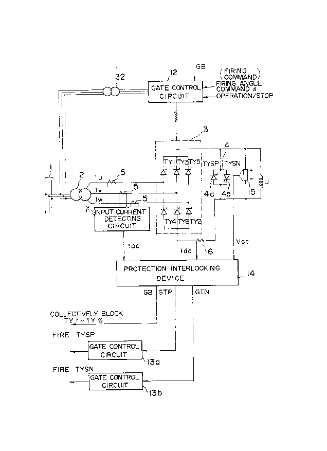
Fig. 1 shows the construction of the first embodiment of a semiconductor
power conversion system according to the present invention.
The system of the embodiment illustrated in the figure is so constructed
that electric power is fed from an AC system 1 to a three-phase bridge
circuit 3 through a power transformer 2, and that a protection interlocking
device 14 is built in.
The three-phase bridge circuit 3 is so arranged that thyristors
15 (hereinbelow, sometimes abbreviated to "TY ') TY1 - TY6 are used as circuit
constituents being semiconductor devices which have a controllable firing
function and a reverse blocking characteristic, and that they are connected in
the form of a bridge. A gate control circuit (firing command circuit) 12 which
pelLol",s the firing controls of the individual thyristors TY1- TY6, is
20 connected to the gates of these thyristors.
The gate control circuit 12 is supplied with AC signals which are applied
through a synchronous transformer 32. It is also supplied with firing angle
commands and operation/stop commands as control signals.
1 4
- 2051030
On the DC side of the three-phase bridge circuit 3, a short-
circuiting switch 4 is connected in parallel with this circuit. The
short-circuiting switch 4 is so arranged that two thyristors are used
as semiconductor devices which have a controllable firing function
5 and a reverse blocking characteristic, and that they are connected in
a reverse parallel relationship to each other as short-circuiting
switches (hereinbelow, sometimes abbreviated to "TYSP" and
"TYSN") 4a and 4b. Gate control circuits 13a and 13b are
respectively connected to the TYSP 4a and TYSN 4b so as to control
10 their on/off operation.
Each of the TYSP 4a and TYSN 4b used is such that its
impedance in its "on" state is lower than the combined impedance of
a path which is to be short-circuited in the bridge of the thyristors
TY1 - TY6.
Besides, in order to produce input signals to the protection
interlocking device 14, this embodiment comprises current
transformers 5 which detect three-phase AC input current values, a
DC current transformer 6 which detects the DC side output current
value Idc, an input current detecting circuit 7 which finds the
2 0 absolute values of the three-phase AC input current values and
delivers the maximum value Iac of them, and a DC voltage
transformer 15 which detects the DC side output voltage value Vdc.
The protection interlocking device 14 supplies the gate control
circuit 12 with a blocking command GB as a signal for controlling the
2 5 operation/stop of the thyristors TY1 - TY6. Likewise, it supplies the
short-circuiting command circuits 13a and 13b with short-circuiting
1 5 ~0~0~
commands GTP and GTN for the thyristor short-circuiting switches
TYSP 4a and TYSN 4b, respectively. That is, the protection
interlocking device 14 constructs protection control means for the
three-phase bridge circuit 3, along with the current transformers 5,
5 DC current transformer 6, input current detecting circuit 7 and DC
voltage transformer 15.
By way of example, a circuit arrangement shown in Fig. 11 can
be used as the input current detecting circuit 7. As illustrated in the
figure, the input current detecting circuit 7 is so arranged that the
10 current signals received from the current transformers 5 are
respectively rectified by rectifier circuits 7a into the absolute
values, which are all applied to a highest value selecting circuit 7b
configured of diodes DI and a variable resistor VR.
Photo-CTs, for example, can be employed as the current
15 transformers 5. They are favorable especially in a case where direct
currents sometimes flow in the three-phase currents Iu, Iv and Iw
transiently .
Next, an example of the protection interlocking device 14, which
is well suited to the present invention including this embodiment,
2 0 will be described with reference to Fig. 2.
Fig. 2 functionally shows the construction of the protection
interlocking device in this embodiment.
The protection interlocking device of this embodiment includes
a detecting function section 140 which detects an internal fault, etc.,
2 5 and a control signal output function section 150 which produces
control signals, such as a blocking command, by the use of the
16 20~i~o~a
detected results.
The detecting function section 140 includes a difference
detecting circuit 141 which detects the difference ~I between an AC
input current Iac and a direct current Idc, a comparator 142 with a
S sign, which produces an internal fault detection signal G86 when the
difference ~I is greater than a preset value K1, a comparator 143
with a sign, which is turned "on" when the difference ~I is smaller
than a minus preset value K2, an overcurrent detector 144 which
produces an overcurrent detection signal when the direct current
1 0 Idc is an overcurrent, an AND circuit 145 which takes the logical
product between the output of the comparator 143 and that of the
overcurrent detector 144, and a comparator 146 which is turned
"on" when the absolute value of a DC side voltage Vdc is equal to or
greater than a preset value V 1.
1 5 The AND circuit 145 produces a commutation failure detection
signal CFD when the comparator 143 is "on", and simultaneously, the
overcurrent of the direct current Idc has been detected by the
overcurrent detector 144.
The comparator 142 functions as an internal fault detector.
2 0 Collectively, the comparator 143, overcurrent detector 144 and AND
circuit 145 function as a commutation failure detector. Further, the
comparator 146 functions as a short-circuit release detector.
The preset value K1 of the comparator 142 is a value which is
set for preventing this comparator from malfunctioning due to a
2 5 measurement error or noise involved in the preceding stage.
Accordingly, an appropriate value is set dependant upon the
1 7 20ri~0~
apparatus to-be handled. Ideally, the value K 1 becomes a value near
to zero. In effect, therefore, the comparator 142 detects that Iac >
Idc holds.
Also, regarding the preset value K2 of the comparator 143, an
5 appropriate value is set for the same reason. In effect, accordingly,
the comparator 143 detects that Iac < Idc holds.
Incidentally, the preset value V 1 of the comparator 146 needs
to be greater than the forward voltage drop of the thyristor TYSP
constituting the short-circuiting switch 4 in Fig. 1.
1 0 The overcurrent detector 144 decides whether or not the direct
current Idc has a magnitude which, when this current flows into the
three-phase bridge circuit 3 in case of a commutation failure, might
damage any of the TY1 - TY6 included in the path of the bridge
circuit. The decision can be made by considering, for example, only
1 5 the value of the current Idc, or the time period of the inflow of the
current Idc into the three-phase bridge 3, along with the current
value.
The control signal output function section 150 includes a
holding circuit 151 which is connected to the output node of the
2 0 comparator 142 and which holds the internal fault detection signal
G86 delivered from the comparator 142 and produces it as a short-
circuiting command GTN, an off-delay timer 154 of preset value Ts
and an off-delay timer 155 of preset value Tp which are connected
to the output node of the AND circuit 145, an inverter 156 which
2 5 inverts the output of the off-delay timer 154, an AND circuit 157
which takes the logical product between the output of the inverter
2~G3~
18
156 and that of the comparator 146, a flip-flop circuit 158 which is
set by the output of the off-delay timer 154 and which is reset by
the output of the AND circuit 157, an OR circuit 152 which takes the
logical sum between the output of the flip-flop circuit 158 and that
S of the holding circuit 151 so as to produce a blocking command GB,
and an OR circuit 153 which takes the logical sum between the
output of the off-delay timer 155 and that of the holding circuit 151
and produces it as a short-circuiting command GTP.
The semiconductor power conversion system shown in Fig. 1,
10 employing the protection interlocking device 14 thus far described,
operates as stated below.
The three-phase bridge circuit 3 has the thyristors TY1 - TY6
fired successively under the control of the gate control circuit 12
and in the combinations of the arms as stated before. Thus, it
15 converts the AC currents Iu, Iv and Iw received through the
transformer 2, into direct currents and feeds a load U with DC
electric power.
At this time, the input currents Iu, Iv and Iw are respectively
detected by the AC current transformers 5, and the one of them
2 0 which has the maximum absolute value is detected and produced as
the AC input current Iac by the input current detecting circuit 7.
Besides, the direct current Idc on the output side of the three-
phase bridge circuit 3 is detected by the DC current transformer 6.
Further, the DC voltage Vdc on the output side of the three-phase
bridge circuit 3 is detected by the DC voltage transformer 15.
The AC input current Iac and the DC output current Idc are
1 9 ~51~3~
applied to the difference detecting circuit 141. The DC output
current Idc is also applied to the overcurrent detecting circuit 144.
Further, the DC voltage Vdc is applied to the comparator 146.
The difference detecting circuit 141 evaluates the difference ~I
5 between the AC input current Iac and the DC output current Idc, and
sends it to the comparators 142 and 143. In the comparator 142, the
difference ~I is compared with the preset value K1. Here, if ~I > K1
holds, the comparator 142 is turned "on" to produce the internal
fault detection signal G86. On the other hand, the comparator 143 is
10 turned "on" if ~I < K2 holds. The "on" output of the comparator 143
is delivered as the commutation failure detection signal CFD from
the AND circuit 145, under the condition that the output of the
overcurrent detector 144 is also "on".
The internal fault is decided upon under the condition of ~I >
15 K1, and this is based on the following reasoning: If the three-phase
bridge circuit 3 is normally operating, the values of the AC input
current Iac and DC output current Idc become equal even during the
commutation, and hence, ~I < K1 holds. However, Iac > Idc holds in a
case where a short-circuit fault ascribable to the semiconductor
2 0 device has occurred in the arms of the three-phase bridge circuit 3,
a case where another circuit has been developed within the three-
phase bridge circuit 3 by any cause, and so forth. Accordingly, when
the condition ~I > K1 is encountered in consideration of the
measurement error etc., which there is allowance for the internal
2 S fault of the three-phase bridge circuit 3 is decided.
Also, the commutation failure is decided upon under the
29~0~a
conditions of ~I < K2 and the detection of the overcurrent by the
overcurrent detector 144, based on the following reasoning: Even in
the absence of any internal fault, the phenomenon of the
commutation failure arises due to a voltage fall on the AC side or a
5 transient current on the DC side. In this case, the relation of Idc > Iac
holds. Besides, at the time of a commutation failure, the direct
current on the DC side flows as a short-circuit current into a short-
circuit having developed within the three-phase bridge circuit 3.
However, considering the facts that, when this current is small, it
10 does not cause the semiconductor devices to malfunction, and that,
when the external fluctuation has become small, the commutation
failure ascribable to the external factor can return into the normal
commutation, the operation of the bridge circuit 3 should preferably
be maintained as it is. Accordingly, in the aforementioned case
15 where ~I < K2 holds and where the current Idc has been detected as
the overcurrent, the commutation failure detection signal CFD is
produced .
When delivered from the comparator 142, the internal fault
detection signal G86 is held by the holding circuit 151.
2 0 Subsequently, this signal is output as the short-circuiting command
GTN directly from the holding circuit 151, as the short-circuiting
command GTP through the OR circuit 153, and as the blocking
command GB through the OR circuit 152.
When delivered from the AND circuit 145, the commutation
25 failure detection signal CFD is held for the preset time period Ts by
the off-delay timer 154, and it sets the flip-flop circuit 158. The
3 ~
21
output of this flip flop circuit 158 is forwarded as the blocking
command GB. The preset time period Ts is set to be, at least, longer
than the turn-off time of each of the thyristors TY1 - TY6, whereby
the commutation failure is terminated without fail.
Simultaneously, the commutation failure detection signal CFD is
held for the preset time period Tp by the off-delay timer 155, and it
is output as the short-circuiting command GTP for short-circuiting
the thyristor TYSP. The preset time period Tp is set to be longer
than the sum of the turn-on time of the short-circuiting switch TYSP
and the operation delay time of the gate control circuit 1 3a,
whereby the short-circuiting operation is initiated without fail.
The blocking command GB is sent to the gate control circuit 12
shown in Fig. 1, and it functions in this case to collectively block the
firing of the thyristors TY1 - TY6. When the blocking command GB is
released, the gate control circuit 1 2 begins to fire the individual
thyristors TY1 - TY6 again.
Regarding the short-circuiting commands GTP and GTN, only the
command GTP is given in the case of the detection of the
commutation failure, and both are given when the fault detection
signal G86 has been output. The reasons for this are as follows:
Regarding the commutation failure, since the short-circuit current
flows in the forward direction of the two arms of the thyristors TYl
- TY6 as shown in Fig. 16 referred to before, the short-circuiting
thyristor switch TYSP 4a arranged in the same direction needs to be
2 5 turned "on" in order to bypass this current, and when the thyristor
switch TYSN 4b in the reverse direction is turned "on", an
2 2 ~ 0 ~
unnecessary short-circuit is formed, and the re-firing of the three-
phase bridge 3 becomes dangerous. Besides, regarding the internal
fault, short-circuit currents can develop in both the directions in
some situations of this fault, so that both the short-circuiting
5 thyristor switches TYSP 4a and TYSN 4b need to be turned "on".
By the way, not only in this embodiment, but also in any other
embodiment, the impedance of each of the thyristors TYSP 4a and
TYSN 4b of the short-circuiting switch 4 is set to become lower than
the series impedance of those two of the thyristors TY1 - TY6 which
10 are parallel to the switching thyristor during the fault. Therefore,
when the short-circuiting switch 4 is turned "on", the short-circuit
current flows through the TYSP 4a or TYSN 4b without fail, and a
bypass circuit is reliably established. Accordingly, any worsening of
the three phase bridge circuit fault is hindered.
Next, the comparator 146 is turned "on" when the absolute
value of the DC side voltage signal Vdc is the preset value V1 or
above. The preset value V1 is set to be greater than the forward
voltage drop of the TYSP constituting the short-circuiting switch 4.
Therefore, when the absolute value of the DC side voltage signal Vdc
2 0 has exceeded the value V1 owing to the turn-off of the thyristor
TYSP 4a in response to the turn-off of the short-circuiting command
GTP, a short-circuit release detection signal as the output of the
comparator 146 is produced. The short-circuit release detection
signal is applied to the AND circuit 157, and it resets the flip-flop
2 5 circuit 158 in conjunction with the "off" state of the off-delay timer
154.
2 3 2 (~
Thus, the blocking command GB having been produced upon the
detection of the commutation failure is released. As regards the
commutation failure, accordingly, if it is temporary, normal
operation can be quickly resumed.
Now, the second embodiment of the semiconductor power
conversion system of the present invention will be described.
This embodiment is constructed as shown in Fig. 1 similarly to
the first embodiment, except that the construction of a protection
interlocking device 14 is different. Here, the point of difference will
1 0 be chiefly described with reference to Fig. 3.
Fig. 3 shows the construction of an example of the protection
interlocking device which is well suited to this embodiment.
The protection interlocking device of this embodiment differs
from the foregoing device shown in Fig. 2, in the constituents which
1 5 function as a commutation failure detector. Accordingly, emphasis
shall be put on this difference in the following explanation.
In this embodiment, the commutation failure detector is
constructed having a comparator 143 which is identical in
construction to the foregoing one shown in Fig. 2, an off-delay timer
2 0 161, a rise detecting circuit 162, a conditional counter 163, and a
comparator 164.
The counter 163 is subject to the condition that it is forcibly
reset to zero when the output signal ST2 of the off-delay timer 161
has become the level "O". This counter 163 counts the number of
2 5 occurances of the PL signal from the rise detecting circuit 162 for a
time period during which the output signal ST2 has the high level
~t5~ 033
24
"1". The resulting count value STX indicates the extent of that
temperature rise of any two of the thyristors of the three phase
bridge circuit 3 which is attributed to a short circuit current flowing
through these devices during the time period specified by the signal
5 ST2.
That is, the count value STX serves as the estimated value of the
device temperature of the two thyristors.
Next, the operation of this embodiment will be described with
reference also to Fig. 4. This figure is a waveform diagram showing
1 0 the operation of the commutation failure detector illustrated in Fig.
3.
When the difference ~I has become smaller than the preset
value K2, the comparator 143 brings its output signal STl to the
"high" level. This signal ST1 is applied to the off-delay timer 161
1 5 and the rise detecting circuit 162. The output signal PL from the rise
detecting circuit 162 and the signal ST2 from the timer 161 are
applied to the conditional counter 163. In this counter 163, the
number of occurances of the signal PL is counted while the output
signal ST2 remains at the "high" level. The counted result STX is
2 0 delivered to the comparator 164.
When the signal STX has reached a present value, which is set
in the comparator 164, this comparator 164 generates a
commutation failure detection signal CFD upon deciding that the
estimated value of the device temperature of the thyristors has
2 5 exceeded a preset limit.
As illustrated in Fig. 4, the counter output STX rises one by one
~0~ 3a
at times tl, t2 and t3. Since, however, the output ST1 of the
comparator 143 remains at the level "O" from time t4 on, the output
ST2 of the off delay timer 161 falls to the level "O" at a time t5 after
Td seconds (the preset value of this timer 161), so that at time t5
5 the counter 163 is reset to the same status as before time tl.
According to this embodiment, the commutation failure
detection can be done on the basis of the estimated value of the
device temperature of the thyristors.
Now, the third embodiment of the semiconductor power
10 conversion system of the present invention will be described.
Fig. 5 shows the construction of the third embodiment of the
semiconductor power conversion system according to the present
nventlon.
The system of the embodiment illustrated in the figure is so
15 constructed that electric power is fed from an AC system 1 to a
three-phase bridge circuit 3 through a power transformer 2, and
that a protection interlocking device 29 is built in.
Likewise to the foregoing one shown in Fig. 1, the three-phase
bridge circuit 3 is so arranged that thyristors TY1 - TY6 are used as
2 0 circuit constituents being semiconductor devices which have a
controllable firing function and a reverse blocking characteristic, and
are connected in the form of a bridge. A gate control circuit (firing
command circuit) 12 which performs the firing controls of the
individual thyristors TY1 - TY6, is connected to the gates of these
2 5 thyristors. Besides, on the DC side of the three-phase bridge circuit
3, the same short-circuiting switch 4 as in the first embodiment is
2 6
connected in parallel therewith.
This embodiment is constructed similarly to the first
embodiment, except that the constructions of the short-circuit
release detector and the protection interlocking device are different.
5 Here, the points of difference will be chiefly described.
In this embodiment, the DC voltage transformer 15 shown in
Fig. 1 is replaced with a DC current transformer 28, which detects
the current It of the short-circuiting switch 4 and applies it to the
protection interlocking device 29.
In the same manner as in the first embodiment, the protection
interlocking device 29 supplies the gate control circuit 12 with a
blocking command GB as a signal for controlling the operation/stop
of the thyristors TYl - TY6. Likewise, it supplies short circuiting
command circuits 1 3a and 1 3b with short-circuiting commands GTP
15 and GTN for the short-circuiting thyristor switches TYSP 4a and
TYSN 4b of the switch 4, respectively.
Fig. 6 shows the functional construction of the protection
interlocking device which is used in this embodiment.
Likewise to the foregoing one 14 shown in Fig. 2, the protection
2 0 interlocking device 29 of this embodiment includes a detecting
function section 140 which detects an internal fault, etc., and a
control signal output function section 150 which produces control
signals, such as the blocking command, depending on the detected
results. The protection interlocking device 29 of this embodiment
2 5 differs from the device 14 shown in Fig. 2, in that the detecting
function section 140 is furnished with a comparator 147 instead of
27 2~3~103
the comparator 146 depicted in Fig. 2.
When the absolute value of the current detection value It of the
short-circuiting switch 4 detected by the DC current transformer 28
is within a preset value Io, the comparator 147 is turned "on" to
5 detect the fact that the short-circuit current has decreased to the
extent that no short-circuiting is required, namely, that it has
become substantially null. The "on" operation of the comparator 147
results in the short circuiting command GTN being reset likewise to
that of the comparator 146. The preset value Io needs to be greater
10 than the detection error of the short-circuit current.
The semiconductor power conversion system of this
embodiment operates similarly to the embodiment shown in Fig. 1,
except that the method of detecting the short-circuit release is
different.
Now, the fourth embodiment of the semiconductor power
conversion system of the present invention will be described.
This embodiment is a system which can cope with a case where
an overvoltage has developed on the DC side of a three-phase bridge
circuit. It is constructed similarly to the first embodiment as shown
2 0 in Fig. 1, except that the construction of the protection interlocking
device 14 is different. Here, the point of difference will be chiefly
described with reference to Fig. 7.
Fig. 7 shows the construction of an example of the protection
interlocking device which is well suited to this embodiment.
2 5 In the protection interlocking device of this embodiment, an
overvoltage detector is provided instead of a commutation failure
28 20~L0~9
detector, but the construction of the remainder of the device is
substantially the same as in Fig. 2. Accordingly, emphasis shall be
put on this difference here.
The protection interlocking device of this embodiment is
S furnished with the overvoltage detector which is constructed having
comparators 148 and 149 and the AND circuit 145.
The comparator 149 functions as a null current detector which
is turned "on" when the absolute value of the DC output current Idc
detected by the DC current transformer 6 is within a preset value Io.
1 0 Besides, the comparator 148 is a comparator with a sign, which is
turned "on" when the DC output voltage Vdc is greater than a preset
value V2. A case where both the comparators 148 and 149 are
turned "on", signifies a situation where the DC voltage Vdc is great in
spite of the direct current Idc being null. Therefore, it is decided
1 5 that the overvoltage has developed due to an abnormality on the
side of the DC load U, and an overvoltage detection signal C59 is
produced from the AND circuit 145.
The control signal output function section 150 has the same
arrangement as in Fig. 2, except that the short circuiting command
2 0 GTN is delivered from the OR circuit 153, while the short-circuiting
command GTP is delivered from the OR circuit 151.
According to such a construction, the overvoltage detection
signal C59 is held for the preset time period Ts by the off-delay
timer 154 so as to afford the blocking command GB. The preset time
2 S period Ts is set to be, at least, longer than the turn-off time of each
of the thyristors TYl - TY6. On the other hand, regarding the short-
~5 i ~
29
circuiting signals, only the signal GTN for short-circuiting the TYSN
4b is output in such a way that the overvoltage detection signal C59
is held for the preset time period Tp by the off-delay timer 155.
The preset time period Tp is set to be longer than the sum of the
turn-on time of the short-circuiting switch TYSN and the operation
delay time of the gate control circuit 1 3b, whereby the short-
circuiting operation is initiated without fail.
The comparator 146 functioning as the short-circuit release
detector is turned "on" when the absolute value of the DC side
voltage signal Vdc is the preset value V 1 or above. The preset value
Vl needs to be greater than the forward voltage drop of the TYSP
constituting the short circuiting switch 4. The output signal of the
comparator 146 having detected the opening or turn-off of the
short-circuiting switch 4 is applied as the reset signal of the flip flop
circuit 158 so as to reset the blocking command GB.
Since this embodiment additionally has the direct current
detection as one of tile conditions of the overvoltage protection
operation, it has the effect of rendering the circuit less prone to
erroneous short-circuiting operations.
2 0 Now, the fifth embodiment of the semiconductor power
conversion system of the present invention will be described.
This embodiment is an example in which the present invention
is applied to a non-circulating current type cycloconverter. More
specifically, as shown in Fig. 8, this embodiment comprises three-
2 5 phase bridges 3a and 3b which are connected in a reverse parallel
relationship to each other. Likewise to the embodiment shown in Fig.
2 0 ~ a
1, it also has an input current detecting circuit 7 connected through
current transformers 5 on the primary side thereof and has a short-
circuiting switch 4, a DC current transformer 6 and a DC voltage
transformer 15 connected on the secondary side thereof.
The three-phase bridges 3a and 3b are connected to common
AC buses, and are respectively subjected to firing controls by gate
control circuits 1 2a and 1 2b in accordance with commands sent from
a control calculation unit not shown. Thus, the former bridge 3a
supplies the secondary side with currents in a positive direction, and
the latter bridge 3b with currents in a negative direction.
Although only the U-phase will be referred to here in this
embodiment, each of the other V- and W-phases is similarly dealt
with. That is, circuit arrangements as described in this embodiment
are juxtaposed for the three phases U, V and W, and the outputs of
the respective circuit arrangements are connected to the secondary
side of a load, for example, a variable-speed generator/motor.
The short-circuiting switch 4 is so arranged that two thyristors
TYSP 4a and TYSN 4b are connected in a reverse parallel
relationship to each other, as semiconductor devices which have a
2 0 controllable firing function and a reverse blocking characteristic.
Gate control circuits 1 3a and 1 3b are respectively connected to the
TYSP 4a and TYSN 4b so as to on/off control them.
In addition, a protection interlocking device 34 is connected to
the output sides of the input current detecting circuit 7, DC current
2 5 transformer 6 and DC voltage transformer 15, and it produces a
blocking command GB and short-circuiting commands GTP and GTN.
31 2a~0~&
The blocking command GB is sent to the gate control circuits 12a and
12b. The short-circuiting commands GTP and GTN are respectively
sent to the gate control circuits 13a and 13b.
An example of the protection interlocking device 34 well suited
5 to this embo~diment will be described with reference to Fig. 9.
Likewise to each of the other protection interlocking devices
described before, the protection interlocking device of this
embodiment is constructed having a detecting function section 140
and a control signal output function section 150.
1 0 The detecting function section 140 includes an absolute value
calculator 141 a which finds the absolute value of a secondary side
output current Idc, a difference detecting circuit 141 which finds the
difference ~ I between the above absolute value and the absolute
value Iac of an AC input current, a comparator 142 which functions
1 5 as an internal fault detector, comparators 143, 144a, 144b and AND
circuits 145a, 145b which function as commutation failure detectors,
comparators 149, 148a, 148b and AND circuits 145c, 145d which
function as overvoltage detectors, and a comparator 146 which
functions as a short-circuit release detector.
2 0 The control signal output function section 150 includes an OR
circuit 151 which holds the output of the comparator 142, an OR
circuit l59a which takes the logical sum of the outputs of the AND
circuits 145a and 145d, an OR circuit 159b which takes the logical
sum of the outputs of the AND circuits 145b and 145c, an OR circuit
2 5 l 59c which takes the logical sum of the outputs of the AND circuits
145a and 145b, and an OR circuit l59d which takes the logical sum
2~0~a
32
of the outputs of the AND circuits 145c and 145d. Besides, this
control signal output function section 150 includes an off-delay
timer 155a in which the output of the OR circuit 1 59a, namely, the
detection signal of a commutation failure or an overvoltage is held
5 for a preset time period Tp, an off-delay timer 1 55b in which the
output of the OR circuit 159b, namely, the detection signal of a
commutation failure or an overvoltage is held for the preset time
period Tp, an off-delay timer 154a in which the output of the OR
circuit 1 59c, namely, the detection signal of the commutation failure
1 0 is held for a preset time period Ts, an off delay timer 1 54b in which
the output of the OR circuit 1 59d, namely, the detection signal of
the overvoltage is held for the preset time period Ts, an OR circuit
159e which takes the logical sum of the outputs of the off-delay
timers 154a and 154b, an inverter 156 which inverts the output of
1 5 the OR circuit 1 59e, an AND circuit 157 which takes the logical
product of the outputs of the comparator 146 and the inverter 156,
a flip-flop circuit 158 which is set by the output of the OR circuit 1
59e, namely, the detection of the commutation failure or overvoltage
and which is reset by the output of the AND circuit 157, namely, the
20 detection of a short circuit release, an OR circuit 1 52 which takes
the logical sum of the output of the OR circuit 151 and that of the
flip-flop circuit 158 so as to produce the blocking command GB, an
OR circuit 153a which takes the logical sum of the output of the OR
circuit 151 and that of the off-delay timer l 55a so as to produce the
2 5 short-circuiting command GTP, and an OR circuit 153b which takes
the logical sum of the output of the OR circuit 151 and that of the
33 2~5 ~
off-delay timer 155b so as to produce the short-circuiting command
GTN.
Here, the comparator 144a as well as the AND circuit 145a and
the comparator 144b as well as the AND circuit 145b are used for
constructing the commutation failure detectors, while the
comparator 148a as well as the AND circuit 145c and the comparator
148b as well as the AND circuit 145d are used for constructing the
overvoltage detectors. The reason therefor is that, since the currents
in the positive direction and the negative direction flow on the
1 0 secondary side, the commutation failures and the overvoltages are
respectively detected with regard to both the currents. Accordingly,
each of the commutation failure detectors or the overvoltage
detectors functions as the commutation failure detector or the
overvoltage detector in any of the foregoing embodiments, except
1 5 for polarities.
Also, the other constituent elements are constructed similarly
and function similarly to the corresponding elements in any of the
foregoing embodiments. Therefore, they shall not be repeatedly
explained here.
2 0 In this embodiment, when the comparator 142 has detected the
internal fault in the way stated before, the internal fault detection
signal is held by the OR circuit 151. Further, the short-circuiting
command GTP is produced from the OR circuit 153a, the short-
circuiting command GTN from the OR circuit 153b, and the blocking
2 5 command GB from the OR circuit 152.
Besides, when the comparators 143 and 144a have detected the
0 3 ~
commutation failure attributable to the three-phase bridge circuit
3a or when the comparators 149 and 148b have detected the
overvoltage attributable to the three-phase bridge circuit 3b, the
off-delay timer 155a is started, and the output thereof is delivered
S as the short-circuiting command GTP from the OR circuit 153a. On
the other hand, when the comparators 143 and 144b have detected
the commutation failure attributable to the three-phase bridge
circuit 3b or when the comparators 149 and 148a have detected the
overvoltage attributable to the three-phase bridge circuit 3a, the
1 0 off-delay timer 155b is started, and the output thereof is delivered
as the short-circuiting command GTN from the OR circuit 153b.
Further, when the output of any of the AND circuits 145a
145d has become the high level, the off-delay timer 154a or 154b is
started, whereby the flip-flop circuit 158 is set, and the blocking
1 S command GB is delivered from the OR circuit 152. By the way, in
this case, when the short-circuit release has been detected by the
comparator 146 subject to the turn-off of the off-delay timer 154a
or 154b, the flip-flop circuit 158 is reset, and the delivery of the
blocking command GB is terminated. On this occasion, when the
2 0 preset time periods are held at Ts > Tp beforehand, the three-phase
bridge circuits 3a and 3b are restored into steady operation states
after the turn off of the short-circuiting switch 4.
In this manner, according to this embodiment, even in the case
where the currents in the positive direction and in the negative
2 5 direction flow on the secondary side, only the switch requiring
short-circuiting is short-circuited, and erroneous short-circuiting
3 5 2 0 ~
operations are avoided.
Moreover, in this embodiment, the internal fault detections,
commutation failure detections and overvoltage detections can be
performed for the two three-phase bridge circuits by employing the
S detectors used in the embodiment shown in Fig. 1, without any
special additional detector, and merely by altering the protection
interlocking device. Also, the operation of the cycloconverter can be
consequently optimalized.
Incidentally, although this embodiment has mentioned the
example wherein the two three-phase bridge circuits are connected
in the reverse parallel relationship, the present invention is not
restricted thereto. By way of example, the present invention is also
applicable to a non-circulating current type cycloconverter wherein
two sets, in each of which two three-phase bridge circuits are
connected in series, are connected in the reverse parallel
relationship to each other.
Although, in the above, the present invention has been
described using several embodiments, it is not restricted to these
embodiments.
2 0 For example, the input current detecting circuit 7 can be
arranged having a sample-and-hold portion in which the AC input
currents detected by the current transformers 5 are sampled at a
preset period, an A/D conversion portion which subjects the
sampled current values to analog-to-digital conversions, a highest
2 S value detecting portion which finds the absolute values of the
obtained digital current values in the respective phases and which
36 ~0~ ~ o-~a
detects the maximum value of them, a signal output portion which
delivers the obtained highest value to the circuit of the succeeding
stage, and a control portion which controls the aforementioned
portions. Besides, these portions can be implemented in the form of
5 an IC.
The various functions can be realized for the respective phases
independently of one another, but they can also be dealt with
through time-division processing by the use of common resources.
In addition, a microprocessor can be built into the control
10 portion or any other constituent, controllable by software, whereby
the protective device can be rendered versatile. By way of example,
the microprocessor can be configured of a CPU which executes
computations and controls, a program memory which stores
programs for controlling the operations of the CPU, a data memory
15 which latches data processed by the CPU, and an I/O interface which
processes signal inputs/outputs from and to the exterior of the
microprocessor.
Further, each of the other constituent elements, for example, the
protection interlocking device 14, gate control circuit 12 and short-
2 0 circuiting command circuit 13 can be constructed of a digital circuit,especially an IC of heightened performance. Besides, the constituent
element can be constructed of a data processor such as
microcomputer, similarly to the input current detecting circuit 7.
Still further, a plurality of circuit elements may well be dealt
2 5 with using a common data processor as resources. By way of
example, the application of a multiprocessor system is considered.
37 2~3~3~
Besides, the protection interlocking device can also be
configured of constituents different from those shown in any of the
foregoing embodiments as long as the same functions are fulfilled.
Also, it is needless to say that the protection interlocking device can
be formed by properly combining the functions of the foregoing
embodiments. By way of example, the commutation failure detector
and the overvoltage detector can be combined.
Although three-phase bridges have been referred to in the
embodiments, the present invention is not restricted to the three
phases. Besides, although the abnormality of the bridge circuit itself
has been exemplified as the internal fault of the bridge circuit, the
present invention is not restricted thereto, but it is also applicable to
a fault with the firing command loop including the gate control
circuits. In this case, means for detecting a pulse anomaly or the like
may well be provided.
The present invention can be extensively utilized for the
controls of an induction machine, a synchronous machine, etc., DC
power transmission, AC-to-DC conversion, DC-to-AC inversion, and so
forth .
2 0 As one application example, a variable-speed generator/motor
set can be mentioned. This equipment is constructed having a
generator/motor whose primary side is connected to an AC system,
and a power conversion system which is configured of power control
devices of reverse parallel connection receiving electric power from
2 5 the AC system and supplying secondary currents to the secondary
side of the generator/motor. By way of example, the equipment is
3 8 21~03&
well suited to a pumping-up power station in which, while running a
pumping water wheel or the like at a variable speed, it controls an
active power output and a reactive power output to stable outputs
even in case of an abrupt change on the AC system side.