Note: Descriptions are shown in the official language in which they were submitted.
20~1103
HIGH 8PR~D CO~PLE~RNTA~Y FIELD ~FF~CT
~RANs~oa LOGIC CIRCnIT~
Field Of The Invention
This invention relates to digital logic
clrcults of the klnd that may be employed in
integrated circuits, and more particularly to high
speed, high density, low power complementary field
effect transistor logic circuits.
Bac~ground Of The Invention
Complementary Field Effect Transistor
(FET) logic circuits, and in particular
Complementary Metal Oxide Semiconductor (CMOS) logic
circuits have become increasingly popular for high
density integrated circuit logic, among other
reasons ~ecause of their high density and low power
dissipation. A typical CMOS logic gate is
illustrated in Figure 1 of U.S. Patent No. ~,911,289
to Takemoto entitled MOS ~ype Semiconductor IC
Device. A CMOS logic gate typically includes a
driving stage having a plurality of FETs of a first
conductivity type connected in parallel and a load
stage comprising a like plura~ity of serially
connected FETs of opposite conductivity type. Each
logic signal input is applied ~imultaneou~ly tô a
pair of transistors, one driver and one load.
Unfortunately, the serial connection of
.25 the load transistors in con~entional CMOS logic
gates reduces the toggle rate or switching speed of
the gate and also reduces the number of inputs which
2051103
--2--
may be applied to the gate (referred to as "fan-
in"). To overcome these problems, an "all parallel"
CMOS logic gate design has heretofore been proposed.
For example, Figure 3A of the aforementioned U.S.
Patent No. 3,911,289 discloses an all parallel logic
gate in which the serial load transistors are
replaced by a first load which may be a MOS
transistor or a resistor and a second load
comprising a MOS transistor having opposite
conductivity type from the driver stage transistors.
The first and second loads are connected in
parallel. A complementary MOS inverter is also
provided between the output of the driving stage and
a voltage source. A similar structure is disclosed
in Japanese Patent 60-236,322 to Yoshida entitled
MOS Transistor Circuit.
While prior art "all parallel" FET
transistor logic circuits may provide some
improvement to the basic CMOS logic gate, the
performance improvement is only about a factor of
two. Moreover, a separate "pull-up" circuit is
needed to raise the output voltage of the gate in
response to an input signal. These pull-up circuits
in the form of resistors or additional transistors
add to the circuit complexity of the logic gate and
also increase the power dissipation thereof.
Attempts have been made to improve the
response of all parallel FET logic without requiring
excessive pull-up power. See for example U.S.
Patent No. 4,649,296 to Shoji entitled Synthetic
CMOS Static Logic Gates. However, as illustrated in
the Shoji patent, highly complex circuits employing
many devices per gate are required, thereby negating
the high density advantage of CMOS logic. Other
attempts have been made to provide improved pull-up
circuits. See for example U.S. Patent 4,053,792 to
Cannistra et al. entitled Low Power Complementary
2051103
--3--
Field Effect Transistor (CFET) Logic Circuit in
which an active pull-up device replaces a passive
resistor. However, this device includes serial load
transistors which negate the advantages of an "all
parallel logic" approach.
U.S. Patent No. 4,390,988 discloses a
multiplexor having a plurality of driving stage FETs
25, 27, and 29 connected between a common output ~7
and a plurality of logic signal inputs Xl, X2 and
XM. IBM Technical Disclosure Bulletin, Vol. 28, No.
6, November 1985, pp. 2576 to 2577 descri~es a
complementary inverter at T3 and T4 for use in a
single ended cascode voltage switch (cvs).
Summary of the ~nvention
It is therefore an object of the present
invention to provide a high speed, high density, low
power dissipation complementary FET logic circuit.
It is another object of the invention to
provide an all parallel FET logic circuit.
It is still another ~bject of the
invention to provide an FET logic circuit which
eliminates the need for power consuming pull-up
circuits.
These and other objects are provided
according to the invention by an FET logic circuit
which comprises a driving stage including at least
one FET of a first conductivity type having at least
one control electrode for receiving logic input
signals. The driving stage F~Ts are connected
between a common output and a first potential level.
A load FET of second conductivity type is provided
and connected between a second potential and the
co,mmon output in an "inverted drain follower"
configuration. A complementary FET inverter is also
provided which comprises an F~T of the first
conductivity type and an FET of the second
conductivity type serially connected between the
20511Q3
-3/1-
first and second potential levels, with the output
of the complementary inverter being connected to the
control electrode of the load FET.
According to the invention, the voltage
s transfer function of the complementary FET inverter
is deliberately skewed, in contrast with a
conventional symmetrical complementary inverter
design. More particularly, the product of the
carrier mobility and the ratio of channel width to
lo length of the inverter FET of said first
conductivity type is so much greater than the
product of the carrier mobility and the ratio of
channel width to length of the inverter FET of said
second conductivity type, so as to achieve a voltage
lS transfer function for said complemêntary FET
inverter which is skewed from a symmetrical transfer
function relative to said first and second potential
levels. In a preferred embodiment this difference is
a factor of four.
FT
- 20slln3
--4--
By skewing the voltage transfer function
of the complementary inverter of the present
invention the voltage lift-off interval for the
logic gate is dramatically decreased thereby
improving the speed of the gate. Moreo~er, if the
inverted drain follower is a depletion mode FET,
additional pull-up transistors or resistors are not
needed. ~he depletion mode FET provides the total
lift-off function by providing a sustaining current
to control snap-off. Power dissipation is thereby
reduced while providing high speed and low device
count. OR and AND circuits-may be provided.
According to another embodiment of the
invention, a second load FET of the second
conductivity type may be provided which is connected
between the second potential level and the common
output, with the control electrode of the second
load being connected to any one of the control
electrodes of the driving stage FETs. The second
load FET provides lift-off current only when the
appropriate control electrode is activated, which
minimizes idle power dissipation while increasing
switching speed. An enhancement mode transistor is
preferably employed.
According to yet another embodiment of the
present invention a second complementary F~T
inverter may be provided in which the voltage
transfer function is maintained symmetrical i.e, it
is not skewed. This second inverter is connected in
parallel with the first inverter, with the output of
2051103
--5--
the second inverter being connected to the control
electrode of the second load FET and its input
connected to the control electrode of the first load
FET. The use of a second inverter also provides a
complement output (i.e. NAND and NOR) for the logic
gate.
The second load FET may comprise a
multigate FET with a respective one of the gate
electrodes being connected to a respective one of
the control electrodes of the driving stage F~Ts.
Although this embodiment provides slightly slower
switching speed because of the serial multigate load
FET, essentially zero power consumption may be
provided. A multigate FET and/or a series-parallel
arrangement of FETs may also be substituted for at
least one of the driving stage transistors to
provide "matrix logic" circuits which implement
complex logic functions.
Brief Description Of The Drawings
Figure 1 is a circuit schematic diagram of
an F~T logic OR circuit according to the present
invention.
Figure 2 is a circuit schematic diagram of
an FET logic AND circuit according to the present
invention.
Figure 3 is a circuit schematic diagram of
an alternate embodiment of an FET logic OR circuit
according to the present invention.
Figure 4 is a circuit schematic diagram of
another alternate embodlment of an FE~ logic OR
circuit according to the present invention.
Figure 5 i5 a circuit ~chematic diagram ~f
yet another alternate embodiment of an FET logic OR
gate of the present invention.
Figure 6 is a circuit schematic diagram of
an FET matrix logic c1rcult accord1ng to the present
invention.
20~1103
--6--
Figure 7 is a circuit schematic diagram of
an alternate embodiment of an FET matrix logic
circuit according to the present invention.
Figures 8A-8B illustrate transfer
functions of complementary FET inverters according
to the present invention.
Figure 9 illustrates the current voltage
transfer function of an inverted drain follower load
transistor according to the present invention.
lo Figure lo illustrates switching diagrams
for FET logic circuits of the present invention.
Figure 11 illustrates the superposition of
sustaining current and inverted drain follower load
transistor current characteristics of the FET logic
circuits of the present invention.
Detailed Description Of The Pre~nt Invention
The present invention now will be
described more fully hereinafter with reference to
the accompanying drawings, in which a preferred
embodiment of the invention is shown. This
invention may, howe~er, be embodied in many
different forms and should not be construed as
limited to the embodiment set forth herein; rather,
this embodiment is provided so that this disclosure
will be thorough and complete, and will fully convey
the scope of the invention to those skilled in the
art. Like numbers refer to like elements
throughout.
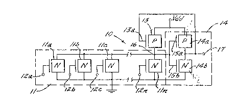
Referring now to Figure 1 an FET logic OR
~0 circuit 10 according to the invention will now be
described. The circuit of Figure 1 includes a
driving stage 11 Which comprises a plurality of N-
type F~Ts lla-lln. ~ach of the driving stage F~Ts
11 includes a control electrode 12a-12n for
receiving logic input signals. The driving stage
FETs 11 are connected in parallel between ground
potential and a common output 16. The driving stage
_7_ 20511Q3
FETs are preferably enhancement type FETs having an
induced channel when the potential at control
electrodes 12a-12n is near ground potential. A P-
type load F~T 13 is connected between the power
supply potential Vtt and the common output 16, in an
inverted drain follower configuration. Logic gate
10 also includes a complementary FE~ inverter 14
including P-type transistor 14a and N-type
transistor 14b. According to the invention, the
o design parameters of translstors l~a and 14b are
skewed so that a skewed complementary inverter
voltage transfer function i5 produced. This skewed
voltage transformer function dramatically reduces
the lift-off interval and eliminates the need for a
separate pull-up transistor as will be described in
detail below. Complementary FET inverter 14 may
also be referred to as a "coupling inverter".
Still referring to Figure 1 the
complementary FET inverter 14 is serially connected
between Vdd and ground, with the output 17 of the
complementary inverter 14 being the output of the
logic gate lo. The output 17 is also connected to
the gate l~a of inverted drain follower load
transistor 13. The gates 15a and 15b of the
complementary inverter are also connected to the
common output 16.
According to the invention, the product of
the carrier mobility and the ratio of channel width
to length of FET 14b is made substantially greater
~0 than the product of the carrier mobility and the
ratio of width to length of the type FET 14a. In
other words, ~l~bZl~b/Ll~b ~ ~lL~ZlLJLl4~ ~ where ~ is the
carrier mobility, z is the channel width and L is
the channel length of respectlve transistors 14a and
~5 14b. By deliberately skewing the voltage transfer
functi~n ~f the c~upling inverter 14, a switching
speed of 500 MHz or greater may be obtained, which
20~1103
--8--
is a factor of five or more than prior art all
parallel logic designs, for example the design
disclosed in the aforementioned U.s. Patent
3,911,289. The skewed complementary inverter design
also dramatically minimizes the need for lift-off
current which increases the power dissipation and
reduces the switching speed of F~T logic circuits.
Referring now to Figure 2 an FET logic AND
circuit according to the present invention is shown.
It will be seen that the circuit of Figure 2 is
identical with the circuit of Figure l except that
the N- and P- devices have been interchanged, and
the ground becomes Vdd and vice versa. As is well
known to those having s~ill in the art, an N-channel
tran~istor is turned on with an up logic level and
off with a down logic level, while a P-channel
transistor is turned off with an up logic level and
on with a down logic level. Accordingly, the
circuit of Figure 2 provides an AND logic function.
The skewed inverter design of transistors 14a and
14b, described in connection with Figure 1, is also
provided in the AND circuit of Figure 2.
Referring now to Figure 3, an alternate
embodiment of an OR logic circuit according to the
present invention is shown. It will be recognized
by those having skill in the art that each of the
circuits of Figures ~-7 may be provided in an AND
configuration by interchanging the N- and P- devices
and voltage terminals. The circuit of Figure 3 is
3 0 identical with the circuit of Figure l except that
an additional lift-off transistor 18 is provided,
the gate 18a of which is connected to one of the
gates 12 of the driving stage FE~s. In Flgure ~
gate 18a is shown conne~ted to gate 12b. According
to the invention, lift-off transistor 18 is
activated when and only when the connected logic
gate 12b is up for an AND gate and ~own ~or an OR
2051103
gate thereby minimi~in~ idle power dissipation while increasing the switching
speed of the logic circuit.
Referring now to Figure 4 another alternate embodiment of an OR
circuit is provided. This circuit is identical to the circuit of Figure 1 except5 lhat a-second coupling inverter 19 and a second load transistor 21 are
provided. Coupling inverter 19 comprises P- transistor 19a and N- transistor
19b, the gates 20a and 20b of which are coupled to gate 13a of inverted drain
follower 13. The output 22 of the second coupling inverter 19 is connected to
a second inverted drain follower 21 which itself is connected between power
10 supply voltage Vdd and common output 16. Accordingly, a compliment
output 22 for the logic gate 10 is provided. According to the invention, the
voltage transfer function of inverter 19 is not skewed; i.e. the transistor
design parameters are subst~nti~lly similar, in contrast wi~ coupling inverter
14 for which the voltage transfer function is deliberately skewed.
Referring now to Figure 5, a hybrid logic circuit is illustrated which is
identical to Figure 3 except that a multigate lift-off transistor 23 is provided.
In a ~refelled embodiment multigate lift-off transistor 23 is a Fermi-FET, as
disclosed in United States Patents 4,984,043, published (issued) 8 January
1991 and 4,990,974, published (issued) 5 February, 1991, both entitled Fermi
20 Threshold Field E~ect Transistor. As illustrated in the aforementioned U.S.
patent 4,990,974, a m~ te Fermi-FET may be provided with diffusion
rails without the need for contact metal, to provide a high speed, high density
device. The gates 23a-23n of multigate Fermi-FET transistor 23 are
, . . .
20S~ 103
connected to a respective gate 12a-12n of the
driving stage transistors lla-lln. The source and
2051103
drain of multigate Fermi-FET 23 are connected
between power supply Vdd and common output 16. The
serial Fermi-FET slightly decreases the switching
speed of the device because the serial gate
structure lowers the llft-off current. However,
because the lift-off current in the serial Fermi-FET
2~ only flows when all of the gates 23a-z3n are
down, all idle power dissipation is eliminated.
Accordingly, total power dissipation is greatly
reduced at a slight speed penalty. The "hybrid"
parallel logic of Figure 5 thereby eliminates all
idle DC power while maintaining high switching rates
at a modest increase in component cost.
Referring now to Figure 6 a matrix logic
implementation is shown. Figure 6 is identical to
the structure of Figure 1 except that the single
gate transistors of driving stage 11 are replaced by
multigate transistors ~la-31n of driving stage 31.
~ransistors 31a-31n are preferably Fermi-F~T
transistors. Transistors 31a-31n each include a
plurality of gates 32~-32z. Accordingly, at a
slight decrease in speed, complex logic functions
may be achieved with great economy of hardware. The
logic gate of Figure 6 implements a sum of products
configuration, i.e. (32a 32b 32c) + (32d-32e-32f) +
. . . (32x 32y 32z).
Referring now to Figure 7, a second matrix
logic implementation is shown. Figure 7 is
identical to the structure of Figure l eXcept that
3~ the ~ingle gate tran~istor of driving stage 11 is
replaced by a multigate transistor 42 and a
SerieS/parallel combination o~ t~ansistors 4~-45 of
driving stage ~1. FFTs 43 and 44 are connected in
parallel with one another and in series with FET 45
between common output 16 and ground. It will be
understood by those having Skill in the art that
other ~ombinations of FETs, in single gate,
-11- 20511Q3
multigate, parallel, series and series/parallel
configurations, may be provided to implement any
desired complex logic function. For example, the
loglc gate of Figure 7 implements the logic function
42a-42b-42c+(43a-45a+44a-45a)+(43a 44a 45a).
Referring now to Figure 8A three
superimposed coupling inverter transfer functions
are illustrated. The central ~urve corresponds to a
balanced coupling inverter design where ~nZ~ =
~pZp/~ where Z and L are channel width and length of
an N-type F~T and P-type F~T and ~ is the
appropriate carrier mobility. It is apparent from
Figure 8A that the coupling inverter output voltage
switches abruptly between voltage l imits at a
specific value of gate inpUt voltage. The maximum
rate of change in output voltage occurs when the
coupling inverter output reaches half of its maximum
value. The input voltage where this rapid voltage
transition occurs is controlled by the physical
dimensions of the P- and N- transistors which
comprise the coupling inverter.
Still referring to Figure 8A, the left
hand voltage transfer function occurs at a
significantly lower value of input voltage than a
2s symmetric inverter design. In this case, saturation
current of the N- channel transistor dominates
saturation current capabilities of the P- channel
device. Specifically, the design criteria at the
left hand curve of Figure 8A is ~nZ~ = 4~n2p/~-
The opposite situation occurs when the P- channel
transistor design dominates saturation current of
the N- channel device The right hand curve of
Figure 8A reflects this design criteria, i. e. ~nZn~
= 0.25~pZp/~-
According to the invention, these skewed
responses are the required design crlteria f~r
complementary lnverter 14 of Figures 1-7. The left
-12- 20~1103
hand voltage transfer curve criteria is a design
criteria for all OR gates, for example as
illustrated in Figures 1, 3, 4, 5, 6 and 7. The
right hand criteria is a design criteria for AND
gates a~ illustrated in Figure 2. If these critical
design criteria are not utilized in the design of
the coupling inverter, switching speed is reduced
and idle power is high negating most of the ~enefits
of all parallel logic. The skewed complementary
inverter design minimizes the "lift-off" time
described below in connection with the "snap-o~f"
property of the present invention. The fast
switching of the skewed inverter design is utilized
to provide all logic circuit~ of the present
invention with maximum switching power and minimum
or zer~ idling power.
Referring now to Figure 8B the current
flowing in the transistors 14a and 14b comprising
the skewed complementary inverter 14 of the present
invention will now be illustrated. This current is
plotted as a function of gate voltage and inverter
design and is normalized to a saturation current of
the N- channel transistor. This transistor current
is not available to charge or discharge circuit
capacity; excess current serves that purpose. The
input voltage to the inverter 14 is the common
output 16. Accordingly, referring to Figure 3,
assuming that common output 16 is at power supply
voltage Vdd, then the inverted drain follower
transistor 13 is on by virtue of the down level of
the inverter output voltage 17 which is coupled to
the gate l~a ~f tranci~tor 1~. Transistor 21 of
~igure 4 would therefore ~e off. When any one of
the driving stage FETs lla-lln are pro~ided with a
~5 p~sitive up level voltage at gate 12a-12n, current
flows throuqh transistor ~3 and the selected driver
transistor 1 ~his current causes the common
2051103
-13-
output 16 to drop. When the common output 16 drops
below a critical value the output 17 of inverter 14
abruptly increases to plus Vtd, shutting off
transistor 13. At the same time, transistor 21 is
switched on.
Referring now to Figure 9, the unique
drain current property of inverted drain follower 13
is illustrated as a function of drain voltage, where
channel length is l~m and channel width is 5~m and
the substrate is doped with 2el6 exceptor ions per
cm3. As shown in Figure 9 the unique characteristic
of inverter drain follower 13 is that zero drain
current occurs at both extremes of drain voltage.
Between these end point voltages a substantial drain
current flows that functions to charge or discharge
circuit capacitances. The area under the curves
shown in Figure 9 is the capacitive charging power.
The amount of available power is controlled by the
physical dimensions of transistor 13.
The zero end point current character of
the inverted drain follower insure~ that no drain
current f lows at either output level of the logic.
No idle power is dissipated by an enhancement
inverted drain follower 13. A depletion mode
inverter drain follower may also be provided in
order to provide the total lift-off function by
providing a sustaining current that controls the
"snap-off" property of the logic circuits of the
present invention. There are two plots illustrated
in Figure 9. For curve A, it is assumed that the
coupling inverter transfer function is linear.
Curve B reflects the actual Fermi-Dirac type of
transfer function typical of a CMOS type inverter.
Referring now to Figure 10 the ~witching
action of logic circuits 10 according to the present
invention is graphically illustrated. Figure 10
shows the combined plots of drain current flowing in
-14- 20511Q3
a l~m N- channel inverted drain follower device 13
driven with different designs of coupling inverter
14, and the drain current flowing in a l~m P-
channel and logic gate input transistor. In both
transistor designs oxide thickness is 120A. As gate
to source voltage ~f the P- channel logic transistor
increases drain current increases and a ~'snap-on"
drain current value is achieved that lnitiates an
irreversible switching action. Snap-on does not
occur for any value of gate voltage below the value
needed to produce snap-on drain current. This
switching property provides the logic circuits of
the present invention with high tolerance to noise
signals.
For switching to occur, the gate voltage
of any selected dri~ing transistor ll mUst be above
the snap-on ~alue. Snap-on voltage is above the
threshold voltage of the driving transistor 11. The
value of the snap-on gate voltage is controlled by
the relative dimensions of the inverter drain
follower 13 compared to any one of the driving
transistors 11. In particular, the product of the
carrier mobility, and the ratio of channel width to
length of the driving transistor 11 is made greater
than the product of carrier mobility and the ratio
of channel width to length of the load FET 13.
Given the drain supply voltage of 5V, snap-on
voltage will be 2.5V if the drain satUration current
of a driving transistor ll is exactly twice that of
~0 the inverted drain follower transi~tor 13.
To turn the logic gate off, when second
load transistor 18 of Figure 3 is switched on by the
action o~ gate 12b ret~rning to the d~wn level, it
provides a sustaining current for logic gate
conduction ~urrent that controls the snap-off
property of the logic gate of the present invention.
W~en on, transistor ~8 proYides idle ~pull-up)
20~1103
-15-
current when the OR gate is on and its output is at
the down level. A similar situation occurs when the
output of an AND gate is at the up level. A typical
sustaining current flowing in transistor 18 is lo ~A
and accounts for power dissipation typically of
about 50 ~watt per logic function. The multigate
configuration of Figure 5 operates as described
above, except no idle power is dissipated at either
logic state up or down.
According to the invention, the need for a
separate lift-off transistor 18 is eliminated by
making the inverted drain follower transistor 13 a
depletion mode device, as shown in Figures l and 2.
When inverted drain follower transistor 13 is a
depletion mode device a prescribed amount of
sustaining current is caused to flow when the gate
voltage of transistor 13 equals its source volta~e.
Figures lOA~ lOB and 11 illustrate the effects of
adding idle current to the inverted drain follower
current voltage profile. A non-zero current is
shown to flow in the circuit when the output
terminal voltage reaches a maximum of vtt. This
current is called the sustaining current and defines
the snap-off current threshold. As gate voltage of
the P- channel logi~ gate, for example, is
decreased, drain current drops. When this current
drops below the sustaining current at the quiescent
ON intercept, the logic output voltage drops along
the contour called the lift-off interval as shown in
Figures lOB and 11. At the end of the lift-off
interval c~rrent flowing in the inverted drain
follower 1 commence~ t~ rapidly switch the logic
circuit to the off state and all current ~low
ceases. In effect, the lift-off interval adds delay
time to overall switching performance and may ~e
used for that p~rpose ln some logic situations.
However~ this delay time must be held to a minimum
-16- 2n5l1 ~3
value by using the skewed inverter design of the
present invention to achieve the maximum switching
rate. The magnitude of the sustaining current is
controlled entirely by the width to length ratio of
the enhancement transistors 18 or 13, when used or
the depletion mode design of transistor 13. Any
value of sustaining current may be selected by the
design of transistor 18 however sustaining current
should be lower than value chosen for the snap-on
current descrioed above in order to preserve the
hysteresis effect.
The snap-off current is usually a fraction
of the snap-on current and accounts for the
hysteresis property of the logic gates of the
present invention. The time the entire circuit
remains in the lift-off interval, TLO~ depends on
capacitive loading C, sustaining current Is and lift-
off voltage interval VLO as follows: TLO = CVLO/IS ~ A
typical logic function lift-off time is 0.5 x lo-9
seconds. Lift-off time depends inversely on the
sustaining current and directly upon the lift-off
voltage interval and therefore can be selected
primarily by the degrees of inverter skew and the
v-alue of sustaining current. once out of the lift-
off interval, the capacitive charging power of theinverted drain follower 13 dominates and overall
very fast switching times result. It is critical
that the lift-off interval be made small by skewing
the voltage transfer function of the complementary
inverter 1~ as has been described above. Otherwise
the virtues of using the inverted drain follower 13
are greatly diminished.
In the drawings and specification, there
have been disclosed typical preferred embodiments of
the invention and, although specific terms are
employed, they are used in a generic and descriptive
sense only and not for purposes of limitation, the
20~1103
-17-
scope of the invention being set forth in the
following claims.