Note: Descriptions are shown in the official language in which they were submitted.
18311
METHOD Of PRODLJCTNG ELECTRONIC, ELECTROOPTICAL
AND OPTICAL COMPONENTS
SPECIFICATION
Field of the Invention
The present invention relates to a method of
producing an article which can be used in the production of
electronic, electrooptical or optical components and,
especially, a crystalline structure or a structure provided
with a crystalline film which can be used for electronic,
electrooptical or optical circuit elements. Specifically
the invention relates to a method of producing a structure
having a crystalline substrate and a crystalline film
deposited on this substrate.
~a~karound of the Invention
The production of articles consisting of a
crystalline substrate and a crystalline film on such
substrate are known to be useful for the production of
electronic, electrooptical and optical components by
semiconductor techniques such as ion implantation and the
deposition of semiconductor elements or the like on such
- 1 -
18311
articles. By and large the quality of the film which may
be the active component of the article is affected by the
characteristics of the substrate. For example, lattice
defects and other lattice parameters of the substrate may
detrimentally affect the crystalline film which is
deposited. A case in point is the fact that epitaxial
deposits on silicon wafers of crystalline films can only be
carried out under special conditions because undesirable
properties or lattice parameters of the wafer can affect
the film or the formation thereof.
For example, if the lattice parameters of the
applied layer are not matched to those of the substrate,
lattice defects can develop at the interface in the newly
formed layer and as this layer grows, these defects will be
propagated and can be dei:rimental to the electrical and
especially the optical characteristics of the layer., Other
approaches such as deposition upon porous silicon have not
been successful in overcoming these problems.
Obj.e~~ of the Inventian
It is, therefore, the principal object of the
present invention to provide an improved method of forming
a monocrystalline film of desired properties on a
crystalline substrate whereby the transmission of lattice
characteristics and especially lattice defects of the
substrate to the newly grown film can be avoided.
- 2 -
~a~~. ~ o~~~
issii
Another object of the invention is to provide a
method which obviates the drawbacks described above.
Summary of the Invention
These objects are attained, in accordance with the
invention by providing a buried amorphous layer on a
crystalline substrate and upon this buried layer a
monocrystalline layer. According to the invention the
monocrystalline layer is transformed into a mixed-crystal
structure or a chemical compound which either corresponds
to the desired crystalline film or, in its lattice
structure, comes closer to the desired crystalline film
than the original mono~rysicalline film. More particularly,
the method of making a crystalline element for an
electronic, electrooptical or optical component comprises:
(a) providing a crystalline substrate having a
buried amorphous layer formed therein and a monocrystalline
layer on the amorphous layer and separated from the
substrate by the amorphous layer: and
(b) transforming the monocrystalline layer into a
mixed-crystal structure or a crystalline chemical compound.
- 3 -
r, , ,
18311
Tn the transformation according to the invention of
the monocrystalline surface layer into an alloy crystal
(mixed crystal) or a crystalline chemical compound, the
nonmatched crystal lattice of the surface layer is
separated by 'the amorphous layer from the substrate and the
transmission of a defect network from the substrate is
,precluded as is the development of a defect network at the
interface with the amorphous layer since there are no
coherent stresses at the crystalline/amorphous interface
which can be transmitted to the newly grown crystal
structure to provide a defect network therein.
The newly formed layer can itself be the desired
product,,i.e. the desired film for electrical, electronic,
electrooptical or optical purposes, or can form a new base
(buffer layer) for the growth of a further layer forming
the desired film. In that case it constitutes a seed layer
for the further monocrystalline growth of the desired film.
The transformation of the monocrystalline layer can
be effected in various ways. It is, for example, possible
to deposit the substances or components of the ,
mixed-crystal or chemical compound upon the monocrystalline
layer and simultaneously or subsequently to heat the layer
to effect thermal diffusion and/or chemical reaction and
homogenization of the crystal layer or the formation of the
mixed-crystal or the chemical compound. I
i
l
18 311 "~, ~ ~ '~
Alternatively, the compounds for the formation of
the mixed-crystal or chemical compound can be applied by
ion implantation in the monocrystalline layer, the ion
implantation being followed by an annealing treatment. In
the formation of the mixed-crystal (alloyed crystal) the
concentrations of the components can be varied in the
direction of growth whereby in a nonideal lattice matched
system in the transformed layer, a gradient of the lattice
parameters in the grown direction can result.
In a further alternative approach to transformation
of the monocrystalline layer, the components required for
formation of the mixed-crystal or the chemical compound can
be deposited by epitaxy and, during or following the
epitaxial deposition, an annealing treatment can be carried
out.
It has been found that, with the present invention,
the lattice parameters of the transformed layer can differ
very significantly from those of the substrate material so
that a substantially higher crystal quality of the
transformed crystal layer can be obtained than with earlier
systems. This layer can have higher temperature resistance
for example.
Through the use of a substrate with an electrically
insulating buried amorphous layer, for example with SIMOX
wafers the new film is dielectrically isolated from the
substrate, the articles made in accordance with the
invention an have all of the inherent advantages of the
SIMOX structure (isolation electronics) for microelectronic
applications, for example high frequency properties.
- 5 -
r
c. '~ ~~ y
~~~~ ? a!:a~
1&311
Brief Description of the Drawinct
The above and other objects, features and advantages
of our invention will become more readily apparent from the
following description, reference being made to the
accompanying highly diagrammatic drawing in which:
FIG. 1 is a diagram illustrating the prior art
approach in which a monocrystalline layer is applied ry
heteroepitaxy to a substrate which has not been lattice
matched therewith; and
FIG. 2 is a diagram showing the approach taken by
the invention.
Specific Description
As can be seew from F~tG. 1, it is not possible to
apply a monocrystalline surface layer of unmatched lattice
parameters to the crystalline structure without the
development of a defect network at the interface 10 or
boundary between the substrate 11 and the monocrystalline
layer 12. In the diagrams of FIGS. 1 and 2 the difference
in lattice structures and parameters is represented by
boxes of different sizes representing, for example, the
crystalline cells.
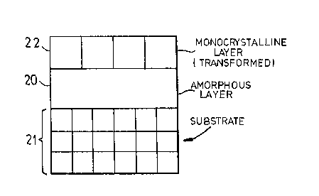
1By comparison, where an amorphous layer 20 is
provided with the substrate 21 and the monocrystalline
layer 22, there is no transmission of defect structures.
- 6 -
18311
The monocrystalline layer or film 22 can thus be
modified as described to form the mixed-crystal or compound
~xamgle ~
Monocrystalline Si-Ge mixed-crystal on Si02
insulating layer.
The substrate is a SIMOX-wafer (SIMOX = separation
by implantation of oxygen). This commercially available
substrate consists of a silicon wafer having a buried
amorphous silicon dioxide layer and a monocrystalline
silicon surface layer.
The monocrystalline silicon surface layer is
initially thinned to a thickness of 20 nm by plasma
etching. The substrate thus prepared is then cleaned in an
epitaxy apparatus by means of molecular beam epitaxy (MBE)
as is common in Si epitaxy to provide a perfect and clean
surface at 450'C, Si and Ge are deposited in a ratio of
80:20. With subsequent tempering at 1100'C for 30 seconds
there is a complete homogenization of the Si seed layer and
the applied Si-Ge film. The resulting Si-Ge layer can be
used directly for Si-Ge electrooptical devices or can serve
as an intermediate layer for further epitaxial growth of
heterostructures and other crystalline structures.
18311
. '~.J
Example 2
Monocrystalline cobalt silicide on silicon dioxide.
The starting material is again a silicon substrate
with buried Sio2 layer, namely, a SIMOX wafer.
The monocrystalline Si surface layer is first
chemically cleaned and then reduced to the desired
thickness by plasma etching. In a vapor deposition
apparatus under ultra high vacuum conditions, Co is
deposited by vapor deposition. Silicide formation is
effected by thermal treatment in the apparatus. The layer
thicknesses depend upon the systems used. CoSi2 resulted
when a 100 nm Si starting layer was coated with 28 nm of a
Co film and after solid body epitaxy had a silicide layer
i.Iuickness of about: 100 nm. For complete reaction of the
CoSi2 layer a temperature of 600°C and 30 minutes was
used. The resulting component had a monocrystalline
silicide layer of especially high electrical and
crystalline quality and an electrically insulating Si02
layer.
_ g _