Note: Descriptions are shown in the official language in which they were submitted.
2~5~
-- 1 --
Optlcal Communication System
Background of the Inventlon
1. Field of the Invention
The present lnvention relates to an optical
communication system based on optical modulation using a
microwave frequency-divislon multiplexed signal and, more
particularly, to an SCM (subcarrier multiplexed) optical
communication system.
The SCM optical communication system has an
excellent feature in that all kinds of signals in either
analog or digital form can be transmitted at the same time and
in large quantities using only a single optlcal carrler. The
present invention employs FM modulation based on direct
modulation by a semiconductor laser, etc., as the optical
modulation ln the SCM optlcal communlcation system. The
present inventlon can be applied to all types of information
communication networks including a conventional optical
communication network, an optical CATV network, a broadband
distribution network mainly handling image information, and
future ISDN (integrated services digital network).
2. Description of the Related Art
Heretofore, wavelength-division multiplexed
transmission has been used mainly for multiplexing
transmltting signals in optlcal communicatlon (such as large-
capacity signal multiplexed transmisslon, in partlcular).
This ls intended for multi-channel transmission wlth optlcal
waves of dlfferent wavelengths (or frequencles) used as
28151-50
2~ ~13 2 5 -
- 2 -
carriers. In the case of an lntensity modulation and direct
detectlon (IM/DM) system, the wavelength-dlvlslon multlplexlng
transmission requires a channel spacing of the order of
several nanometers in wavelength so that channels can be
distinguished from each other by optical filters. In the case
of a coherent optical communicatlon system, a channel spaclng
is presently required which ls of the order of ten and several
times the blt rate because the ability to control crosstalk
between ad~acent channels is limited. In the case of, for
example, high-speed multlplexed transmlssion at a bit rate ln
the order of glgablts, the channel spaclng ls about 20 GHz. A
recelver whlch can detect all of the channels slmultaneously
cannot be realized. However, the number of channels to be
multiplexed may be lncreased at the sendlng end. Therefore,
only one channel can be recelved at a tlme.
On the other hand, the conventlonal SCM optlcal
communlcatlon system, uses malnly an intenslty modulatlon
system, based on the dlrect modulatlon of a semlconductor
laser as lts optlcal modulatlon system and a dlrect detection
system using a PIN photodlode or APD as its recelvlng system.
By way of example, a conventlonal FDM (frequency-
divislon multlplexed) optlcal transmisslon system and a
conventlonal TDM (tlme-dlvislon multlplexed) optlcal
transmlsslon system are lllustrated in Figure 1 and Flgure 2,
respectively. In both systems, coherent transmlsslon of four-
channel, 622 Mb/s signals is made, and the optical
transmission capaclty ls 2.5 Gb/s.
28151-50
3 ~ ~
-- 3
In the optical FDM system, as can be seen from
Flgure 1, optlcal modulators 1-1 to 1-4, whlch correspond ln
number (four in thls example) to channels and have optlcal
carrlers of dlfferent frequencles Fsl to Fs4, each produce a
modulated optlcal slgnal. These modulated slgnals from the
optlcal modulators are mixed ln an optlcal coupler 2 to
produce a frequency-dlvision multiplexed optical signal whlch,
ln turn, ls transmitted through an optical flber 3. At the
receivlng end, the optlcal signal transmitted through the
optlcal flber ls mlxed with a local llght source
(semlconductor laser) and
28151-50
- 4 - ~ 3 ~ ~
heterodyne detected by means of 4, an optical
receiver 5 and an amplifier 6, whereby it is converted
to an electric intermediate frequency signal. The
resulting electric signal is then filtered by a
bandpass filter 7 to allow only the signal on a
desired channel to pass. The signal is then
demodulated by a demodulator 8.
In the TDM optical transmission system, as can be
seen from Figure 2, signals transmitted on channels
are time-division multiplexed by a multiplexer (MUX )
11 to produce a time-division multiplexed signal
which, in turn, modulates an optical modulator 12.
The modulated signal is transmitted through an optical
transmission fiber 13. At the receiving end, the
optical signal transmitted from the transmitting end
is optical-heterodyne detected by the use of a local
light source (semiconductor laser) 14, an optical
receiver 15 and an amplifier 16 for conversion to an
electric signal. The resulting electric signal is
filtered by a bandpass filter 17 to pass intermediate
frequency signals of all the channels (bandwidth is
about 25GHz x 2). These signals are demodulated by a
demodulator 18 and then separated by a demultiplexer
( DEMUX ) 1 9 into the signals for the respective
channels
~ ~ 5 'll 3 ~ 5
-- 5
A problem wlth such a conventional optical
frequency-division multiplex transmisslon system as shown in
Figure 1 is that, since the channel spacing at the time of
signal multiplexing must be large, of the order of ten and
several times the blt rate, multiplexed signals cannot be
detected simultaneously at the recelvlng end. However, the
number of channels to be multlplexed may be increased at the
transmitting end, but a limited number of channels that can be
detected actually. In the case of hlgh-speed transmission of
digital data (gigabit transmisslon) in partlcular, be only one
channel that can be detected at a time by a recelver. Also,
the number of channels whlch can be multlplexed ls llmited by
the band of frequencies over whlch a semiconductor laser
serving as a local llght source ls tunable.
An optical time-divlslon multlplex transmlssion
system such as that shown ln Figure 2 requlres a multlplexer
for time-divislon multiplexlng and a demultiplexer for
separatlng the components in a time-division multiplexed
signal transmitted over an optical transmission line. These
circuits are very expensive. The use of these clrcults will
lead to an increase of cost of the whole system. Moreover,
the heterodyne detector requires a demodulatlon bandwldth
whlch is wlde enough to cover all the channels that are
multiplexed.
The conventlonal SCM optlcal communlcatlon system
described above requlres that the llght output be llnear wlth
the lntensity modulatlon of the semiconductor laser. Thls
28151-50
- 6
sets a limit to the bandwidth for modulation. Under the
present clrcumstances, the bandwldth ls ln the order of 1 to 2
GHz at best. Thus, the wldeband transmlsslon is apt to be
influenced by signal distortion, thus limltlng the capaclty of
transmlsslon informatlon. This makes lt dlfficult to meet the
requlrements of future large capaclty communlcatlons.
Moreover, slnce the dlrect detection system alone can be used
as the detection system, lt ls dlfflcult to achleve a
sufflcient receiver sensitlvlty. Therefore there are llmlts
to transmlssion dlstance and the number of signals to be
distributed.
If, therefore, optical angular modulation could be
used as the optical modulation ln the SCM optlcal
communlcatlon system, such technlcal problems would be solved.
In this case, however, to achleve a hlgh recelver sensltlvlty,
the coherent optlcal transmlssion system must be used, whlch
requlres an
28151-50
~ ~ _ 7 _ ~ 2 ~
optical heterodyne receiver or an optical homodyne
receiver, which have complex structures. It also
requires countermeasures against degradation of the
receiver sensitivity due to fluctuations in the state
of polarization of signal light and local light.
This will make the receiver very expensive. It is
difficult to u~e SUCll an expensive receiver in
subscriber systems.
Summary of the Present Inventlon
It is an object of the present invention to
provide an optical comlllunication system which permits
large-capacity frequency-division multiplexed optical
transmission to be implemented easily and at a low
cost and a number of channels to be received
simultaneously by a single receiver.
It is another object of the present invention to
provide an optical communication system which permits
SCM optical communication by coherent optical
transmission to be implemented at a low cost.
A feature of the present invention resides in
an optical communication system characterized by
allocation of transmission signals to more than one
channel at different microwave frequencies, providing
modulators for modulating carriers of the microwave
frequencies with tlle translllissic,n signals and band-
3 ~ ~
-- 8
llmlting filters placed in the preceding stages or succeeding
stages of sald modulators, combinlng band-limited and
modulated transmlsslon signals to produce a microwave
frequency-dlvlslon multlplexed slgnal, frequency modulating an
optlcal frequency modulator with the multiplexed signal to
produce an optical frequency modulated signal, optically
transmlttlng the optical frequency modulated slgnal, detectlng
the optically transmltted optlcal signal to thereby convert it
to an electrlc slgnal, separatlng the electrlcal slgnal into
channels by bandpass fllters and demodulating each of the
signals separated into channels.
In accordance with the present lnventlon, there is
provided an optlcal communicatlon system for transmltting a
slgnal llght carrylng a plurallty of data signals from sending
equlpment to receivlng equipment, said sending equipment
comprising:
a plurality of optical frequency modulated signal
generating units, each comprising:
a plurality of modulators modulatlng carrlers having
different microwave frequencies with a plurality of
transmlsslon slgnals and outputting first transmission
signals;
a plurality of band limiting fllters band limitlng one of
the data slgnals and the flrst transmlsslon signals, and
outputting second transmission signals;
adding means for generatlng a microwave frequency
multlplexed slgnal by addlng the second transmission slgnals;
D 28151-50
- 8a
and
an optical frequency modulator generating an optlcal
frequency modulated slgnal by frequency modulation with said
mlcrowave frequency multlplexed slgnal; and
optical mlxlng means for mlxlng each optlcal frequency
modulated slgnal generated by the optlcal frequency modulator
ln sald plurality of optlcal frequency modulated signal
generating units and for generatlng an optical frequency
multiplexed signal to be transmitted to the receiving
equipment.
In accordance with another aspect of the invention,
there is provlded an optical communicatlon method for
transmitting signal light having a first polarization state
includlng the steps of:
a) mlxlng the slgnal llght and local light havlng a
second polarlzatlon state, after the flrst and second
polarlzatlon states have been made colncldent wlth each other,
and produclng mlxed llght;
b) optlcally transmlttlng the mixed light as
~0 transmitted optical light; and
c) detectlng an intermedlate frequency element produced
by a dlfference between a frequency of the slgnal light and a
frequency of the local light.
In accordance wlth another aspect of the invention,
there is provlded an optlcal communlcation method for
transmitting more than one optical signal having optlcal
carrlers of dlfferent frequencles lncludlng the steps of:
28151-50
- 8b -
a) mixlng each of the more than one optlcal slgnal and
a correspondlng one of local llght slgnals after polarlzatlon
states of one of correspondlng more than one optlcal slgnal
have been made colncldent wlth each other, and produclng a
multlplexed optlcal slgnal;
b~ optlcally transmlttlng the multlplexed optlcal
slgnal; and
c) detectlng an lntermedlate frequency element produced
by a dlfference between a frequency of each of the more than
one optlcal slgnal and a frequency of the correspondlng one of
the local llght slgnals.
In accordance wlth another aspect of the lnventlon,
there ls provlded an optlcal communlcatlon method lncludlng
the steps of:
a) allocatlng transmlsslon slgnals on more than one
channel havlng different mlcrowave frequencles;
b) modulatlng carrlers of the microwave frequencles
with the transmlssion slgnals for produclng modulated slgnals;
c) combining the modulated transmlsslon slgnals for
~0 produclng a multlplexed slgnal;
d) modulatlng an optlcal frequency modulator wlth the
multlplexed slgnal for producing a modulated optical slgnal;
e) mlxlng the modulated optlcal slgnal wlth local llght
wlth thelr polarlzatlon state made colncldent wlth each other
and optlcally transmittlng the mlxed llght;
f) detectlng an lntermedlate frequency element produced
by a dlfference between a frequency of the modulated optlcal
28151-50
2 ~
- 8c -
signal and a frequency of the local llght to thereby convert
the modulated optlcal slgnal to an electrlcal slgnal;
g) extracting correspondlng channel signals from the
electrlcal signal by electric fllters; and
h) demodulating each of the correspondlng channel
signals.
In accordance wlth another aspect of the invention,
there ls provlded an optlcal communication system for
transmltting a signal light having a plurality of data signals
from sending equipment to receiving equipment, the sending
equipment comprising:
a plurality of optical modulated signal generating units,
each comprising
a plurality of modulators modulating carriers having
different microwave frequencles with transmlsslon signals and
outputtlng frequency modulated signals;
addlng means for generatlng a mlcrowave frequency
multiplexed signal by adding the frequency modulated signals;
and
an optical frequency modulator generating an optical
frequency modulated signal by frequency modulation with said
microwave frequency modulated signals;
optical mixing means for mlxlng each said optical
frequency modulated signal generated by said optical frequency
modulator in said plurality of optical frequency modulated
signal generating units and generating an optical frequency
multlplexed signal; and
28151-50
' $
- 8d -
an optical frequency discrlminator, connected to said
optlcal mixing means, receiving and divlding the optical
frequency multiplexed signal into two signals, a first one of
the two signals having a time delay wlth respect to a second
one of said two signals, and mixing the two signals to
generate an optical frequency multiplexed slgnal to be
transmltted to the receivlng equlpment.
In accordance wlth another aspect of the lnventlon,
there is provlded an optical communicatlon system for
transmlttlng to recelvlng equlpment a slgnal llght optlcally
modulated by a mlcrowave frequency multlplexed slgnal, and
optical communication system comprislng:
sendlng equipment optlcally modulating the signal light,
sald sending equipment comprlslng:
a plurality of optlcal frequency modulated signal
generatlng unlts, each optlcal frequency modulated signal
generating unlt comprislng:
a plurallty of modulators modulatlng carrlers of
different mlcrowave frequencles wlth each of transmlsslon
slgnals correspondlng to the carrlers;
addlng means for generatlng a mlcrowave frequency
multlplexed slgnal by addlng modulatlon slgnals output by sald
plurallty of modulators; and
an optlcal frequency modulator generatlng an optlcal
frequency modulated signal by frequency modulation with sald
frequency multlplexed slgnal;
optlcal mlxlng means for mlxlng each optlcal frequency
28151-50
~ 5 ~ ~ 2 ~
- 8e -
modulated slgnal generated by sald plurallty of optlcal
fre~uency modulated slgnal generatlng unlts and for generatlng
an optical frequency multlplexed slgnal; and
an optlcal frequency dlscrlmlnator dlvldlng the optlcal
multiplexed slgnal lnto a flrst slgnal and a second slgnal,
the flrst slgnal being delayed by a delay tlme wlth respect to
the second slgnal, and for generatlng the optical frequency
multiplexed signal to be transmitted to said recelving
equipment by mlxlng the first slgnal and the second slgnal.
In accordance wlth another aspect of the present
invention, there ls provlded an optlcal communlcatlon system
for transmitting a signal light carrying a plurality of data
signals from a single transmltter to receiving equipment, said
transmitter comprlslng:
a plurallty of optical frequency modulated signal
generatlng unlts, each comprising:
a plurality of modulators modulatlng carrlers havlng
dlfferent mlcrowave frequencies wlth a plurallty of
transmlsslon slgnals and outputtlng flrst transmlsslon
slgnals;
a plurality of band limiting filters band limiting one of
the data slgnals and the flrst transmlsslon signals, and
outputting second transmlssion slgnals;
addlng means for generatlng a mlcrowave frequency
multlplexed slgnal by addlng the second transmlsslon slgnals;
and
an optlcal frequency modulator generating an optlcal
28151-50
- 8f -
frequency modulated signal by frequency modulatlon wlth sald
microwave frequency multlplexed slgnal; and
optical mlxing means for mlxlng each optlcal frequency
modulated signal generated by said optlcal frequency modulator
ln said plurality of optlcal frequency modulated slgnal
generatlng unlts and generatlng an optlcal frequency
multlplexed slgnal to be transmltted to the recelvlng
equlpment.
In accordance wlth another aspect of the lnventlon,
there ls provlded a sending device for transmlttlng a signal
llght carrying a plurality of data signals to a receiving
devlce ln an optlcal communlcatlon system, comprlslng:
a plurallty of optlcal frequency modulated slgnal
generatlng unlts each comprislng:
a plurallty of modulators modulatlng carriers having
different mlcrowave frequencles wlth a plurality of
transmlsslon signals and outputting first transmission
slgnals;
a plurallty of band llmltlng fllters band llmltlng one of
the data slgnals and the flrst transmlsslon slgnals, and
outputtlng second transmlsslon slgnals;
addlng means for generating a microwave frequency
multlplexed slgnal by addlng the second transmission signals;
and an optlcal frequency modulator generatlng an optlcal
frequency modulated slgnal by frequency modulation with said
microwave frequency multlplexed slgnal; and
optlcal mlxlng means for mlxlng each optlcal frequency
28151-50
- 8g -
modulated slgnal generated by sald optlcal frequency modulator
ln sald plurallty of optlcal frequency modulated slgnal
generatlng unlts and generatlng an optlcal frequency
multlplexed slgnal to be transmltted to the recelvlng devlce.
Brlef Descrlptlon of the Drawlngs
Flgure 1 ls a block dlagram of a conventlonal
optlcal FDM system for transmlsslon of four-channel 622-Mb/s
slgnals;
Flgure 2 ls a block diagram of a conventlonal
optical TDM system for transmlsslon of four-channel 622-Mb/s
signals;
Figures 3 to 6 lllustrate the fundamentals of
optical communicatlon systems of the present inventlon;
Figures 7A to 7C lllustrate the channel allocation
ln the optical communlcatlon systems of the
28151-50
- 9 ~
present invention;
Figure 8 illustrates a general spectrum of a
modulated signal;
Figure 9 illustrates frequency allocation at the
5 IF stage of an SCM optical heterodyne detection system
of the present invention;
Figure 10 is a block diagram of an optical
communication system according to a first embodiment
of the present invention;
Figure 11 illustrates a specific arrangement for
four-channel 622-Mb/s signal transmission according to
the first embodiment;
Figure 12 illustrates an arrangement of the
receiver in a second embodiment of the optical
15 communication system of the present invention;
Figure 13 illustrates an arrangement of the
receiver according to a third embodiment of the
optical communication system of the present invention;
Figure 14 is a diagram for use in explanation of
20 the principle of the frequency discrimination in the
third embodiment;
Figure 15 is a block diagram of a first
embodiment of an optical exchange system of the
present invention;
Figure 16 is a block diagram of a second
- 10 ~ 2 ~
embodiment of the optical exchange system of the
present invention;
Figure 17 is a block diagram of a fourth
embodiment of the optical communication system of the
5 present invention;
Figure 18 is a block diagram of a fifth
embodiment of the optical communication system of the
present invention;
Figure 19 is a block diagram of a sixth
10 embodiment of the optical communication system of the
present invention;
Figure 20 is a block diagram of a seventh
embodiment of the optical communication system of the
present invention;
Figure 21 is a block diagram of an eighth
embodiment of the optical communication system of the
present invention;
Figure 22 is a block diagram of a ninth
embodiment of the optical communication system of the
present invention;
Figure 23 is a block diagram of a tenth
embodiment of the optical communication system of the
present invention; and
Figure 24 is a block diagram of an eleventh
embodiment of the optical communication system of the
3 ~ ~
present invention.
Detailed Description of the Preferred Embodiments
The present invention is an improvement on the
conventional SCM optical communication system and its
basic configurations are illustrated in Figures 3 to
6.
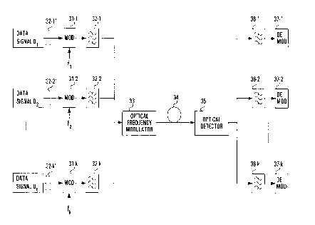
Referring first to Figure 3, at the transmitting
end, microwave carrier frequencies f1 to fk are
10 allocated to channels (the number of channels is
supposed here to be k), respectively. In modulators
(MOD) 31-1 to 31-k, the carriers of f1 to fk are
modulated with data signals D1 to Dk on the channels.
The modulated carriers output from the modulators 31-1
15 to 31-k are filtered by bandpass filters 32-1 to 32-k,
respectively. The output signals of the filters are
added together to produce a microwave frequency-
division multiplexed signal, which, in turn, frequency
rnodulates an optical frequency modulator 22. The
20 frequency modulated signal output from the optical
frequency modulator is translnitted over an optical
transmission fiber 34.
At the receiving end, the optical signal
transmitted over the optical fiber is detected by an
25 optical detector 35, whereby it is converted to an
B
3 2 ~
- 12 -
electric signal. The resulting electric signal is
applied to bandpass filters 36-1 to 36-k for
separation into channels. The output signals of the
bandpass filters 36-1 to 36-k are demodulated by
5 demodulators (DEMOD) 37-1 to 37-k, respectively.
In the other system of Figure 4, at the
transmitting end, there are provided n optical
frequency-modulated signal generating sections A1 to
An each of which is the same in arrangement as the
transmitter of Figure 3 constructed from the
modulators 31-1 to 31-k, the bandpass filters 32-1 to
32-k and the optical frequency modulator 33. However,
the optical frequency modulators 33 in the optical
frequency-modulated signal generating sections A1 to
15 An have their respective optical carriers of different
frequencies fs1 to fsn The optical frequency-
modulated signal generating sections A1 to An produce
their respective optical frequency-modulated signals
in the same manner as in Figure 3. The optical
frequency-modulated signals are mixed in the optical
combiner or coupler 38 to produce an optical
frequency-division multiplexed signal which, in turn,
is transmitted over the optical transmission fiber 34.
At the receiving end, the optical frequency-
25 division multiplexed signal is detected by the optical
- 13 -
detector 35, whereby it is converted to an electric
signal. The resulting electric signal is applied to m
bandpass filters 36-1 to 36-m, which correspond in
number to all the channels or part of the channels,
5 for separation into channel components. The channel
components are demodulated by demodulators 37-1 to 37-
m.
In the arranyements of Figures 3 and 4, the
modulators 31-1 to 31-k may employ any of analog and
10 digital modulation systems which include amplitude
modulation (AM), frequency modulation (~M), phase
modulation (PM), intensity modulation, amplitude-shift
keying (ASK), frequency-shift keying (FSK), phase-
shift keying (PSK), etc. All the modulators 31-1 to
15 31-n are not required to employ the same modulation
system, but more than one modulation system may be
employed in combina~ion.
As the optical frequency modulator 33, use may be
made of a semiconductor laser (a broadband DFB type
20 semiconductor laser, in particular). In this case,
the direct modulation of its bias current permits the
optical frequency modulation.
As the detection system in the optical detector
35, use may be made of an optical heterodyne or
25 homodyne detection system using local light, a direct
7 ~ ~ ~
detection system using optical filters, a detection
system using an optical freyuency discriminator, etc.
In the case of the direct detection system using
optical filters, the electrical bandpass filters 36-1
to 36-k become unnecessary, but as many optical
filters as there are channels and demodulators
succeeding the respective optical filters are needed
instead. In the case of the optical heterodyne
detection system, by adjusting the oscillation
10 frequency of its local light source, it becomes
possible to select a channel among channels. In this
case, only one set of a bandpass filter and a
demodUlator has to be provlde~ to follow the
optical detector 35, irrespective of the number of
channels.
The optical communication system shown in Figure
3 or Figure 4 may be employed to implement an optical
exchange system or an optical switching system. That
is, the optical exchange system is implemented by
20 inputting the demodulated signals in the optical
communication system to an electronic exchange system
having as many input/output ports as there are
channels and performing arbitrary exchanges of
channels. In addition, the optical exchange system
25 will also be implemented by dividing the optical
- 15 ~
signal transmitted in the above-described optical
communication system into as many optical signals as
there are transmission channels using branch lines,
optical-heterodyne detecting the separate optical
5 signals using separate local light emitters and
selecting an arbitrary optical signal from the optical
signals.
Next, Figure 5 illustrates an application of the
SCM optical communication system of the present
10 invention to an optical distribution network. As
shown in the figure, in a transmitting station A,
which may be a central office or a head end, different
microwave carrier frequencies f1 to fk are allocated
to channels (here their number is k) carrying data
15 signals D1 to Dk and the carriers of frequencies f1 to
fk are modulated by the data signals D1 to Dk,
respectively, in modulators 41-1 to 41-k. The
modulation system in this case may be any of ASK, FSK,
PSK, AM, FM, PM, etc. Subsequently, the resulting
20 modulated signals are added together in a combiner 42,
such as a multiplexer, thereby producing a microwave
frequency-division multiplexed signal. The
multiplexed signal modulates (AM, FM, PM, etc.) an
optical modulator 43. The resulting modulated optical
25 signal (SCM optical signal) is transmitted over an
- 16 ~
optical transmission fiber 44.
The optical signal output from the transmitting
station A is transmitted to each subscriber C via a
repeater station B which is generally a local office,
a hub, a remote terminal, etc. In the present
invention, in the repeater station B, the optical
signal transmitted from the transmitting station A and
local light output from a local light source 45 which
is common to all the subscribers C are mixed in an
optical mixer 46 and the mixed signal branches off
from an optical branch unit 47 to the subscriber
stations C.
In each subscriber station C, the optical signal
transmitted from the repeater station B is detected by
an optical detector 48, whereby it is converted to an
electric signal. The electric intermediate frequency
signal is applied to electric bandpass filters 50-1 to
50-k via an amplifier 49, thereby separating the
channel components in the optical signal. The channel
components are demodulated by demodulators 51-1 to 51-
k.
In the above arrangement, by transmitting a light
signal obtained by coupling light sighals modulated
with SCM signals in the optical modulators having
different carrier frequencies, wavelength (frequency
- 17 ~ 3 ~ ~
of light)-division multiplex transmission of coherent
SCM optical signals is made possible.
To implement a bi-directional optical
transmission system, the arrangement of Figure 5 may
be modified such that a different microwave carrier
frequency is allocated to each of subscribers, each
carrier is modulated with a signal from a
corresponding respective subscriber to produce a
10 modulated signal, an optical modulator is modulated
with the modulated signal to produce an optical
modulated signal, and the optical modulated signal is,
in turn, transmitted as an up signal.
Next, Figure 6 illustrates a coherent optical
15 transmission system of the present invention which
incorporates countermeasures against polarization
fluctuation.
As shown ln Flg. 6, ln a transmltter T, a
modulated optical signal obtained by modulating a
20 transmission liyht source 61 with a data signal D and
a local optical signal output from a local light
source 62 are mixed in an optical mixer 64 after their
polarization states have been made to coincide with
each other by a ~olariza~.ion controller 63. The
25 resultant mixed li~htwave trarIslllitted over an optical
fiber 65.
t.i~
- 18 -
In a receiver R, the optical signal transmitted
over the optical fiber is optical-heterodyne detected
by an optical receiver 66 for conversion to an
electrlc signal. The resultant IF signal ls sent
5 via an amplifier 67, an electric filter 68, etc., to a
demodulator 69.
This arrangement, which uses an optical
heterodyne detection system, may also be modified to
use an optical homodyne detection system by making a
transmission optical signal and a local optical signal
coincident with each other in their frequency and
phase.
The arrangement of Figure 6 may be modified to
permit coherent wavelength (frequency of light) -
division multiplexed transmission by transmitting
light subjected to wavelength synthesis after
polarization synthesis to a plurality of transmission
light sources having different oscillation
wavelengths.
The arrangement of Fiyure 6 may be applied to
such an SCM optical communication system as shown in
Fiqure 5. Moreover, it may be applied to a
wavelength-division multiplex transmission system for
coherent SCM optical signals.
In the arran~emerlts of Figures 5 and 6, as the
modulation system use may be made any of analog and
digital modulation systems which include amplitude
modulation (AM), frequency modulation (FM), phase
modulation (PM), intensity modulation, amplitude-shift
keying (ASK), frequency-shift keying (FSK), phase-
shift keying (PSK), etc. All the modulators need not
employ the same modulation system, but more than one
modulation system may be employed in combination.
As the optical modulator, use may be made of a
semiconductor laser (a broadband DFB type
semiconductor laser, in particular), an LiNbO3 optical
modulator, etc. In the case of the coherent optical
system in particular, as the modulation system, use
may be made of any of coherent modulation systems such
as amplitude modulation (AM), frequency modulation
(FM), phase modulation (PM), etc.
In addition, as the optical receiver, use may be
made of an optical heterodyne or homodyne receiver or
a receiver using optical filters.
In the arrangements of Figure 3 and 4, carriers
of different frequencies f1 to fk allocated to the
respective channels are modulated with data signals D1
to Dk, respectively, and the resultant modulated
signals are made to pass through bandpass filters 32-1
to 32-k and then combined (frequency-division
- 20 -
multiplexed). The spectrum of the data signal and the
frequency allocation to channels in the present case
are illustrated in Figures 7A to 7C. Here, the
channel spacing and the bandwidth of each of the
bandpass filters are selected to avoid crosstalk
between adjacent channels.
In general, the spectrum of a modulated signal
has a shape such as that shown in Figure 8 which has
high-order Bessel function components centered at
multiples of the frequency of a data signal around the
carrier frequency. The spectrum of Figure 8
corresponds to the case where a carrier having a
frequency of fc is modulated with a frequency B.
Thus, the bandwidth of each bandpass filter is
selected to reject components which overlap the
bandwidth of an adjacent channel. In practice, in
order to increase the number of channels, it is
desired that bandpass filters each having as narrow a
bandwidth as possible be used. For example, in the
case of Figure 8, it is common to pass a component
ranging from fc-B to fc+B, the so-called main lobe
component. Therefore, the frequency range from fc-B
to fc+B may be selected as the bandwidth of the
bandpass filter. The channel spacing in the
25 frequency-division multiplexed signal obtained by
2 1 ~ ~m~
synthesizing signals which passed through the bandpass
filters 32-1 to 32-k can be put close up to twice the
bit rate in the case of a digital signal. Therefore,
it becomes possible to easily produce a high-density
frequency-division multiplexed signal.
In the above, a description was made of the
method by which a modulated signal on each channel was
subjected to bandpass filtering. Instead, use may
also be made of a method by which an original data
signal is subjected to lowpass filtering before
modulation.
That is, a data signal (a baseband signal), if it
is a digital signal at a bit rate B, has such a
Bessel-function-like spectrum as shown in Figure 7A.
Thus, by extracting only the main lobe component (0 <
f < B) by the use of a lowpass filter and then
modulating a carrier with the main lobe component, a
modulated signal which is the same as that when
bandpass filtering is used will be obtained as shown
20 in Figure 7b-
If such modulated signals are added together,
then such a SCM signal as shown in Figure 7c will be
obtained.
According to the present invention, as described
25 above, a frequency-division multiplexed signal is
-
- 22 -
produced by electric stages and then an optical
carrier signal is frequency modulated with the
frequency-division multiplexed signal in the optical
frequency modulator 33, whereby an optical -modulated
signal is produced. Hence, only one optical modulator
suffices.
Since, as described above, the channel spacing
can be set narrow, about twice the bit rate at the
transmitting end, a wideband receiver can be used at
the receiving end for receiving all the channels or
more than one channel at a time, permitting a
considerable increase in the number of channels that
can be received.
Moreover, according to the present invention, the
15 frequency-division multiplexing can be implemented by
the use of an inexpensive multiplexer such as a
microwave combiner or coupler. That is, there is no
need for an expensive multiplexer required of time-
division multiplexing. This enables optical
20 communication systems to be constructed at a very low
cost.
Next, in the arrangement of Figure 5, carriers of
frequencies f1 to fk allocated to channels are
modulated with data signals D1 to Dk, respectively,
25 and then synthesized (frequency-division multiplexed).
- 23 ~
The frequency allocation to channels in the frequency-
division multiplexed signal in this case will also be
shown as in Figures 7A to 7C. The channel spacing
needs to be selected to avoid crosstalk between
adjacent channels. However, by lowpass filtering only
the main lobe component of a data signal (baseband
signal) or by bandpass filtering only the main lobe
component after modulation, it becomes possible to put
the channel spacing close to about twice the data rate
in the case where digital signals are handled.
1 0
Next, the optical modulator 43 is subjected to
modulation with the multiplexed signal and then an
optical modulated signal is transmitted optically.
The modulated light is mixed with local light common
to subscribers in the repeater station B and then
branches to each subscriber. Subsequently, the
modulated light is heterodyne detected by the optical
receiver 48 in each subscriber's station. The
resultant IF signals are separated for each of
channels and then demodulated. For information, in
Figure 9 there is shown an example of frequency
allocation at IF stage in the case where frequency
modulation (FM) is produced in the optical modulator
43.
In the case of usual optical heterodyne
- 24 - ~ 2 ~ ~
detection, in order to make the power input to an
optical receiver as large as possible, the local light
source is generally placed in the neighborhood of the
optical receiver. In an optical subscriber system,
5 however, the distance between a repeater station B and
a subscriber C is no more than several kilometers
A loss caused by optical transmission over the
distance is in the order of 1 dB tin the case where a
single mode fiber is used). Thus, as in the present
10 invention, the local light source 45 can be placed in
the repeater station B to permit parallel transmission
to subscribers C by the use of direct fiber branching.
In order to suppress the deterioration of receiver
sensitivity to the utmost, it is only required that
15 the branching loss be compensated for by an optical
amplifier.
According to the present invention, as described
above, a single local light source 45 placed in the
repeater station B permits simultaneous optical
20 heterodyne reception by more than one subscriber C.
Therefore, cost per subscriber is reduced considerably
and a low-cost coherent optical SCM network is
implemented.
Moreover, since, as described above, the ch~nnel
25 spacing can be narrowed up to about twice the data
2 5 ~ ~a
signal rate at the transmitting end, the receiving end
is allowed to use a wideband receiver for simultaneous
reception of all the channels or more than one
channel. This permits a marked increase in the number
5 of channels which can be received. This possess a
great advantage over the wavelength-division multiplex
transmission in the conventional coherent optical
communication system in which there is a limit to the
number of channels that can be received at one time.
Next, in the arrangement of Figure 6, the local
light source 62 is placed in the transmitting station
T, transmission light and local light are mixed after
their polarization states have been made coincident
with each other and the resultant IF signal is
15 transmitted optically. Thus, the countermeasures
against polarization fluctuation can be taken without
imposing a burden of cost on the receiver R. In other
words, stable reception is allowed without depending
on the polarization state of transmission light.
In the case of usual optical heterodyne
detection, in order to make the power input to an
optical receiver as large as possible, the local light
source is generally placed in the neighborhood of the
optical receiver as described above. In an op~ical
25 subscriber system, however, the distance between a
- 26 _ ~ 7 ~
transmitting station and a subscriber is relatively
short and the loss of the local light is not large.
Thus, the arrangement of Figure 6 is possible.
Where the present invention is applied to an
5 optical distribution system, the arrangement of Figure
5 is suitable when the transmitting station is
relatively distant from subscribers because it is
desired that the local light source and the optical
receiver be placed as close to each other as possible
10 in terms of optical loss as described above. On the
other hand, where subscribers are relatively close to
the transmlttlng statlon, the use of the arrangement
of Flgure 6 ls sultable.
~lereinafter, preferred embodilllents of the present
invention will be described with reference to the
drawings .
Figure 10 is a block diagram of a first
embodiment of an optical communication system
according to the pre~n~ inven~ion. This embodiment
uses an optical heterodyne detection system as the
detection system at the receiving end.
At the transmittinc~ end, carriers of frequencies
f1 to fk allocated to chdnnels are modulated with data
signals D1 to Dk in modulators 31-1 to 31-k,
respectively. The resultant modulated signals are
filtered by bandpass filters 32-1 to 32-k. Here, as
the modulation system used in the modulators, use may
be made of any of frequency modulation (FM), amplitude
modulation (AM), phase modulation (PM), intensity
5 modulation, amplitude-shift keying (ASK), frequency-
shift keying (FSK), phase-shift keying (PSK), etc.
Depending on transmission signals, the modulation
system may vary between channels. The channel spacing
and the bandwidth of each of the bandpass filters are
10 selected to avoid crosstalk between adjacent channels
in the multiplexed signal as shown in Figures 7C and
8. In particular, each of the bandpass filters is
designed to have a narrow bandwidth of fc ~ B to fc +
B.
Instead of using the bandpass filters, lowpass
filters may be used to filter original data signals
prior to modulation.
Subsequently, the signals allowed to pass through
the bandpass filters are synthesized in a multiplexer
20 71 to produce a frequency-division multiplexed signal.
The multiplexer has only to have a function of merely
adding electrical signals together. For example, use
may be made of a simple and inexpensive device such as
a microwave coupler. The resultant multiplexed signal
25 is used to frequency-modulate an optical frequency
- 2~
modulator 33, thereby producing modulated light. The
modulated light is transmitted over an optical
transmission fiber 34. A semiconductor laser is used
as the optical frequency modulator 33. The direct
5 modulation of a bias current of the laser will produce
frequency modulation.
Next, at the receiving end, an optical heterodyne
detector 35 comprises a local light source
(semiconductor laser) 72, an optical receiver 73 and
10 an amplifier 74, whereby the light signal transmitted
from the transmitting end is optically heterodyned.
The frequency allocation at the IF stage after the
optical heterodyne detection is the same as in Figure
9. An electrical signal resulting from the heterodyne
15 detection branches to channels and is then filtered by
bandpass filters 36-1 to 36-k, thereby deriving
corresponding respective channel signals. The channel
signals are demodulated by demodulators 37-1 to 37-k.
The present invention is compatible with coherent
20 detection, such as optical heterodyne detection, as
compared with the conventional SCM-AM (IM) modulation
system, and the optical heterodyne detection is
permitted as in the present embodiment. Thus, not
only can a high receiver sensitivity be achieved
easlly, but all of the channels falllng wlthln the
- 29 -
bandwidth of the optical receiver 73 can be received
simultaneously. This possesses a great advantage over
the optical frequency-division multiplex transmission
in the conventional coherent optical communication
5 system in which the number of channels that can be
received at a time is limited to one. Therefore, not
only can the transmission distance be increased, but
also the number of channels that can be received can
be increased considerably.
Here, to make the function and effect of the
present embodiment definite, a comparison will be made
between four-channel 622-Mb/s signal transmission
shown in Figure 11 and the conventional coherent
transmission shown in Figures 1 and 2. In both cases,
15 each of the number of channels, the bit rate and the
optical transmission capacity (2.5 Gb/S) is the same.
In the first place, comparing the present
embodiment with the optical FDM system of Figure 1, in
order to transmit 2.5-Gb/s information, the present
20 embodiment needs only one optical modulator, while the
optical FDM system needs as many optical modulators as
there are channels. However, the present embodiment
needs an optical modulator with a wider frequency
response characteristic. That is in the order of 6-8
25 GHz, which may be achieved for example by a
- 30 -
multielectrode DFB type semiconductor laser.
Therefore, the present embodiment has a great
advantage that transmission can be made by using one
optical modulator.
In addition, in the present embodiment, the
channel spacing at the transmitting end can be as
small as approximately twice the bit rate, as
described above. Therefore, the use of a wideband
(approximately 10 GHz) receiver permits simultaneous
10 reception of all of channels or more than one channel.
Of course, as in the optical FDM system, the selective
reception of only one channel is also possible.
Next, making a comparison between the present
embodiment and the TDM optical transmission system,
15 the present embodiment can implement frequency-
division multiplexing with a multiplexer such as a
microwave coupler, while the TDM optical transmission
system needs an expensive multiplexer for time-
division multiplexing. Moreover, as the demodulation
20 bandwidth of the optical heterodyne detector, the
present embodiment needs only the bandwidth required
of each channel, while the TDM optical transmission
system needs a bandwidth which is wider than that
required of each channel by a factor of the number of
25 channels. In addition, an expensive demultiplexer is
- 31 -
required to separate the channels.
As can be seen from the foregoing, compared with
the conventional multiplexing optical transmission
system, the present embodiment permits a very simple,
5 inexpensive, large-capacity optical transmission
system .
Figure 12 is a block diagrarn of the receiving end
according to a second embodiment of the optical
communication system of the present invention.
As shown ln Flgure 12, in thls embodlment, the
light signal transmitted from the transmitting end
shown in Figure 10 over the optical transmission fiber
34 is applied to an optical branch unit 81, so that it
divides into a plurali ty of channels . O~tical filters
1 5 82-1 to 82-]c separate the optical channel components,
which are, in turn, sub jected to direct detection in
optical receivers 83-l to ~33-k, whereby they are
converted to electric signals.
The present embodill)ent also permits an optical
20 transmission system to be implemented, which is very
simple in structure, low in cost and large in capacity
as compared with the conventional multiplexed optical
transmission system.
Figure 13 is a bl ock diagram of the receiving end
25 according to a third ernbodiment of the optical
~ i
- 32
communication system of the present invention.
In this embodiment, the light signal transmitted
from the transmitting end shown in Figure 10 over the
optical transmission fiber 34 branches into channels
5 through an optical branch unit 81. The optical signal
components of channels are separated and direct-
detected by optical frequency discriminators 91-1 to
91-k. The arrangement of the optical frequency
discriminators is well known. As an example, a
10 discriminator using an optical delay circuit is
described herein. That is, the input optical signal
(coherent light) is divided into two channels, thereby
causing two optical signals I1 and I2 to pass through
optical paths 101 and 102, respectively, so as to
15 delay the optical signal I2 by a time &S with respect
to the optical signal I1. Subsequently, the two
optical signals I1 and I2 are mixed again in an
optical mixer 103 and the mixture is converted to an
electric signal by an optical receiver 104. The
20 principle of the frequency discrimination in this case
will be described below with reference to Figure 14.
Let the frequency of the input optical signal I
be fs~ Then
I = cos (2~ ~ s l ~ s (l)) ~(l)
25 where ~s(t) stands for the phase.
~n
~ 33 ~
Supposing the dividing ratio to be A : B, I1 and
I2 are glven by
I, .--J~ cos (2 1~ r s L ~ s ( l ) ) ~ ~ ('~),
1 2 '= r3 cos (2 1t r s (l - r) ~ s (l- r)) (3)
Thus, photocurrent J output from the optical
receiver 104 will be given by
J -- C -1- 2 ~ ~ co~ 7C r s r -1- ~ 5 (l) - ~ S (L - T )) ~ ' (4)
In this equation, constant and higher frequency
components are neglected.
From equation (4), J varies with fs with a period
of 1/ ~-' as shown in Figure 14. As can be seen from
this relationship ~etween J and fs~ frequencies in the
range from Y point to Z point can be discriminated
with a point X (corresponding to frequency fso) set as
5 a reference pOil1t. By setting the reference point of
each of the optical frequency discriminators 61-1 to
61-k to a different frequency, the frequency
discrimination can be performed for each of the
channels.
Figure 15 is a block diagram of a first
embodiment of an optical exchange system of the
present invention.
In this embodiment, an electronic exchange unit
111, which has as many input/output ports (k x k) as
there are transmission channels (K), is disposed to
7 ~ J
- 34 -
succeed the demodulators 37-1 to 37-k at the receiving
end in the optical communication system shown in
Figure 10, thereby making exchanges of channels. That
is, signals recovered by the demodulators can be
5 exchanged by the electronic exchange unit 111.
The mere placement of an electronic exchange unit
to succeed the demodulators in the optical
communication system of the present invention permits
an optical exchange system to be implemented easily.
1 0 If, in the arrangement of Figure 15, an electronic
switch is disposed in place of the electronic exchange
unit 1 1 1, an optical switching system can be
implemented which permits switching between channels.
Figure 16 illustrates a second embodiment of the
15 optical exchange system of the present invention.
In thi s embodiment, as many optical heterodyne
detectors each having a separate local light source as
there are channels are provided at the receiving end
to thereby implement a k x k coherent optical exchange
20 system. That is, the optical signal transmitted from
the transmitting end shown in Figure 10 is divided
into as many optical signals as there are transmission
channels ( k in number ) . The divided optical signals
are heterodyne-detected by their respective optical
25 heterodyne detectors 122-1 to 1 22-k having their
respective local light sources producing different
frequencies fL1 to fLk and an arbitrary channel is
selected to thereby make an exchange of channels.
In the arrangement of Figure 15, channel exchange
5 is implemented by using the electronic exchange unit
111. In the present embodiment, on the other hand,
the channel exchange is implemented by tuning the
oscillation wavelength of the local light source of
each of the optical heterodyne detectors 122-1 to 122-
10 k and selecting a desired channel. In the presentembodiment as well, an optical switching system can be
lmplemented by switchlng between channels.
The transmitter in each of the above embodiments
uses the principle of the transmitter shown in Figure
15 3. If the principle of the transmitter shown in
Figure 4 is used instead, the transmission of more
channels will be implemented.
Figure 17 illustrates a fourth embodiment of the
optical communication system of the present invention.
20 In this embodiment, an optical amplifier 130 for
compensating for brarlching loss is disposed between
the optical mixer 46 and the optical branch unit 47 in
the repeater station B in the arrange~ent shown in
Figure 5.
In Figure 17, in the transmitter A, carriers of
B
- 36 - J ~
different frequencies f1 to fk allocated to channels
are modulated with data signals D1 to Dk in the
modulators 1-1 to 1-k. Here, the modulation system
used in the modulators 41-1 to 41-k may be any of
5 amplitude modulation (AM), frequency modulation (FM),
phase modulation (PM), intensity modulation,
amplitude-shift keying (ASK), frequency-shift keying
(FSK), phase-shift keying (PSK), etc.
_ Modulated signals obtained from the modulators
10 are combined by a combiner, such as a microwave
coupler, to produce a frequency-division multiplexed
signal. The channel spacing of the multiplexed signal
is selected to avoid crosstalk between adjacent
channels. As me~ans therefor, a lowpass filter may be
15 used to allow only the main lobe component of each
data signal to pass or a bandpass filter may be used
to allow only the main lobe component of each data
signal to pass after modulation. Subsequently, the
multiplexed signal thus obtained is used to modulate
an optical modulator 43 and the resultant modulated
light is transmitted over an optical fiber 44. As the
optical modulator 43, use may be made of a
semiconductor laser or a LiNO3 modulator. As the
modulation system used in the optical modulator 43,
use may be made of any of coherent modulation systems
- 37 ~
including amplitude modulation, frequency modulation,
phase modulation, etc.
The optical signal transmitted from the
transmitting station A in that way is transmitted to
5 the repeater station B through the optical fiber 44.
In the repeater station B, the incoming signal light
is mixed in the optical mixer 46 with local light
emitted from a local light source (for example, a
semiconductor laser) 45 which is common to
10 subscriber's stations and then the resultant light is
amplified by the optical amplifier 130 consisting of a
fiber type light amplifier or a semiconductor light
amplifier. Subsequently, in the optical branch unit
47 the amplified light branches into subscriber's
15 stations C through optical fibers.
In each subscriber's station C, the optical
signal transmitted from the repeater station B is
converted to an electric signal, whereby it is
heterodyne detected. Subsequently, the resultant IF
signal is amplified by the amplifier 49 and then
divides into channels. The bandpass filters 50-1 to
50-k separate channel signal components in the IF
signal and then the channel signal components are
demodulated by the demodulators 51-1 to 51-k.
According to the present embodiment, only one
- 38 -
local light source 45 provided in the repeater station
B permits simultaneous optical heterodyne reception
for more than one subscriber. Therefore, each
subscriber's station needs no local light source and
5 hence the cost per subscriber can be reduced to a
large extent.
Moreover, the loss due to optical branching can
easily be compensated for because the mixed light is
amplified by the light amplifier 130 provided in the
10 repeater station B before optical branching.
Of course, it is also possible to compensate for
branching loss by a light amplifier provided for each
of transmission lines after optical branching by the
optical branch unit 47 instead of providing the common
5 light amplifier 130 followed by Lhe optical branching
unit. Further, the light amplification may be
provided before and after branching.
Next, countermeasures ayainst polarization
fluctuation for carrying out the present invention
20 will be considered. In order to carry out the optical
heterodyne receptlon, the slgnal llght and the
local llght must be colncldent wlth each
other in the state of ~olarization. If they are not
coincident with each other, for example, in an extreme
25 case, in the case of linear polarization in which they
~: i
- 39 -
are perpendicular to each other in polarization, the
receptlon ls lmposslble. As countermeasures
against such problems, there will be methods of using
(1) a polarization preserving fiber, (2) a
5 polarization diversity reception system, (3) a
polarization active control reception system, (4) a
polarization scrambling system, etc. In (1), the
polarization preserving fiber is not suitable because
it is expensive and fibers which have already been
installed become unavailable. In (2), the
polarization diversity reception is promising for
usual coherent optical transmission systems, but a
subscriber's receiver needs a dual configuration,
increasing its cost. In the present invention, a
local light source and a receiver are away from each
other and thus it is difficult to feed an IF signal
back to the local light source. Thus, (3) and (4)
will be considered hereinafter.
Figure 1~ is a block diagrarn of the repeater
station B according to a ~ifth embodiment of the
optical communicatioll sysl~ of the present :invention.
This embodiment us~s tl-lt: me~hod (3), i.e., the
polarization active controL receptlon system as the
countermeasures against polarization.
As shown in the figure, in the repeater station
7 -
- 40 -
B, the signal light transmitted from the transmitting
station A shown in Figure 17 and local light obtained
from the local light source 45 via a polarization
controller 131 are mixed in a 2 x 2 optical coupler
132 and then divided into two branches. A signal on
one of the branches is transmitted to subscriber's
stations and the other is used as a monitor signal for
polarization control.
For polarization control, the other signal from
10 the optical coupler 132 is subjected to heterodyne
detection in an optical rece~iver 133. At this point,
as a detected slgnal, a 0 th-order beat slgnal (maln-
carrier component) or one-channel component in the SCM
signal is derived througl1 a bandpass filter 134. The
15 power of the IF signal t}lUS obtained is measured by a
power meter 135 and tl-e measured value is then
compared with a reference value by a comparator 136.
Based on the difference between the measured value and
the reference value, the polarization controller 131
20 is controlled by a polarization control circuit 137 to
match the polarization state of the local light to
that of the signal light, and the oscillation
frequency of the local light source 45 is controlled
by an AFC circuit 138, thereby maximizing the power of
the IF signal. Such feedback to the polarization
.
~ j .
- 41 -
state of the local light and the oscillation frequency permits
very good receiver sensltlvlty.
As the sequence of feedback control ln thls case,
using a slgnal swltchlng unlt, the dlfference slgnal f-rom the
comparator 136 ls flrst applled to the polarization control
clrcuit 137 to thereby perform the polarlzation control by the
polarlzation controller 131, and then the difference signal is
applied to the AFC circuit 138 to thereby control the
oscillation frequency of the local light source 45.
As the polarization controller 131, for example, A
/4 (quarter-wavelength) plate and A / 2 (half-wavelength)
plate may be used in combination.
Figure lg is a block dlagram of a sixth embodlment
of the optlcal communlcation system of the present invention.
Thls embodiment uses the above method (4), i.e., the
polarlzation scrambling system as countermeasures against
polarization.
As shown in the flgure, a polarlzation scrambler 139
is dlsposed to follow the optlcal modulator 43 ln the
transmlttlng statlon A shown in Figure 17, thereby scrambling
the polarization in the modulated optical slgnal obtained from
the optical modulator prior to optlcal transmission thereof.
Although there ls some reduction in recelver sensltlvlty, such
scrambling of
28151-50
- 42 -
polarization permits polarization-insensitive optical
heterodyne reception.
Figure 20 illustrates a seventh embodiment of the
optical transmission system of the present invention.
5 This embodiment is directed to a bi-directional
optical communication network using the optical
communication system shown in Figure 17.
In this embodiment, subscriber stations C1,
C2,...., Cn are allocated different carrier
10 frequencies fs1, fs2,...., fsn. The carrier is
modulated with a subscriber's data signal in a
modulator 141, and the resultant modulated signal is
used to modulate an optical modulator 142 for data
transmission. The modulated optical signal from the
optical modulator 142 is transmitted, as an up signal,
from an optical coupler 143 to the repeater station B
over the same route as the down line. In this case,
as the optical modulator 142, use may be made of an
inexpensive semiconductor laser for low-speed optical
modulation because the transmission distance is short,
and the data signal from each subscriber is usually
not of large capacity. As the modulation system,
amplitude modulation will be used.
The optical signal from each subscriber station
is converted to an electrical signal by an optical
receiver 144 in the repeater station B. A signal of
frequencies allocated to each subscriber C is detected
by a bandpass filter 145. The resultant RF-signal
combined signal (SCM signal) modulates an optical
5 modulator 146 for up signals. The modulated optical
signal is coupled with the optical fiber 44 by an
optical coupler 147 for transmission to the
transmitting station A over the optical fiber.
In the transmitting station A, the transmitted
10 optical signal branches in an optical branch unit 148
and then detected by an optical receiver 149. As the
optical modulation and detection system in this case,
use may be made of the coherent modulation and
demodulation system as in the case of the down signal
15 or the amplitude modulation - direct detection system
if the speed of the up signal is low in comparison
with the down signal.
According to the present embodiment, a bi-
directional optical communication network can be
implemented at a very low cost because the arrangement
in which a single local light source 45 common to all
the subscriber stations is installed in the repeater
station permits bi-directional optical ~ommunication.
Of course, an up signal from each subscriber can
25 also be used as a request signal to the repeater
44
statlon B or the transmltting station A. With the above
arrangement, all of the channels can be received by each
subscrlber station. Where there are too many channels or each
subscriber's receiver has an lnsufflclent bandwidth to cover
all the channels, the request signal can be used to tune the
osclllatlon frequency of the local llght source 45 to select a
desired channel. In this case, however, more than one local
llght source would be required in the repeater station B.
In the above fourth to seventh embodiments, a slngle
transmisslon llght source (optical modulator 43) is used. The
use of two or more transmisslon llght sources with different
oscillation frequencles to transmit llght composed of optlcal
slgnals each modulated with an SCM signal as in the above
embodiments permlts wavelength-dlvlslon multlplex transmission
of coherent SCM optical signals. Optical communication of
still larger capacity is made posslble.
Next, a descrlption will be made of embodlments
lncorporatlng countermeasures agalnst polarlzation which
permit a more inexpensive coherent SCM optical transmission
system.
Figure 21 illustrates an eighth embodiment of the
~'
28151-50
- 45 -
optical communication system of the present invention.
The present embodiment is an application of the
arrangement shown in Figure 6 to the SCM optical
transmission system.
As shown in Figure 21, in the transmitting
station A, a modulated optical signal (SCM optical
signal) output from the optical modulator 43 is mixed
with the local light output from the local light
source 62 in the outical n~i~er 64. Before mixing, the
local light is made coincident with the modulated
signal in polarization in tlle polarization controller
63. The mixed light is transmitted over the optical
fiber 44.
The optical signal thus transmitted optically
branches in the optical branch unit 47 in the repeater
station B placed in the neighborhood of subscribers
for fiber transmission to eacl1 subscriber.
In each subscriber station C, as in the above
elnbodimel1ts, the o~ticdl sigl1al transmitted frorn the
repeater station B is cor-verted to an electric signal
by the optical receiver ~8, whereby it is l~eterodyne
detected. The resultant Il~ signal is separated into
Cllarlllel COIIII~On~lltS by LJdll~lL~SS filters, and then the
channel components are delllodulated by their respective
delnodulators-
t~ i
- 46 ~
There is no need for an optical branch if transmission
is made between one transmitter and one receiver.
According to the present embodiment, since the
local light source 62 is installed in the transmitting
5 station A, the transmission light and the local light
are mixed after they have been made coincident with
each other in polarization, and the resultant mixed
optical signal is transmitted. The countermeasures
against polarization in the coherent SCM optical
10 transmission system can be implemented without
irnposing a burden of cost on each subscriber C.
To counter polarization, use may be made of a
polarization active control receiving system such as
that shown in Figure 18 or a polarization scrambling
system such as that sl-lown in Figure 19. With the
former system, although it has high receiver
sensitivity, there is some increase in cost because it
is technically difficult to implement the polarization
controller 131 which traces random variations in
polarization. With the latter, it is somewhat
difficult to implement the polarization scrambler 139
which can take sufficient measures against high-speed
transmission. ~owever, the systerll used in the present
embodiment has no such problems and can implement a
polarization-independent coherent SCM optical
~ ' i
.....
- 47 -
transmission system at a low cost corresponding to a
network.
Figure 22 illustrates a ninth embodiment of the
optical communication system of the present invention.
5In this embodiment, a light amplifier 150 is
installed as a post amplifier in the transmitting
station A.
According to this arrangement, the power of a
signal from the transmitting station A is amplified,
10 thus increasing the system margin, the transmission
distance and the number of branches.
Figure 23 illustrates a tenth embodiment of the
optical communication system of the present invention.
In this embodiment, a light amplifier 151 is
15 installed in the preceding stage of the optical branch
unit 47 in the repeater station B in the arrangement
of Figure 21.
According to this arrangement, branch loss caused
by the optical branch unit 47 can be compensated for
20 by the light amplifier 151, thus permitting an
increase in the number of branches.
Following the branching process by the optical
branch unit 47, a light amplifier may be used for each
line. In this case, though an improvement is made in
25 receiver sensitivity, as many light amplifiers as
- 48 - ~ ~ 5 ~
there are subscribers will be needed. In addition,
light amplifiers may be provided in the preceding and
succeeding stages of the optical branch unit.
Furthermore, these arrangements and the arrangement of
5 Figure 22 may be used in combination.
Figure 24 illustrates an eleventh embodiment of
the optical communication system of the present
invention. This embodiment is arranged such that an
angle modulated optical signal is converted to an
10 intensity modulated optical signal which is
subsequently transmitted.
As shown in the figure, in the transmitting
station T, an SCM optical signal resulting from
production of optical angle modulation (FM, PM) in the
15 optical modulator 43 is transmitted over the optical
fiber after being converted to an amplitude modulated
optical signal by an optical frequency discriminator
152.
In the receiver R, the optical signal transmitted
20 from the transmitting station is converted to an
electrical signal by the optical receiver 66, and the
resultant RF signal is applied via the amplifier 67 to
an RF demodulator 153 where it is demodu~ated.
As described so far, the present invention is
25 permltted to use any of AM, FM and PM as lts
- 49 ~
optical modulation system. As described in the
Related Art, the amplltude modulatlon, when it ls
produced by intensity modulation of a semiconductor
laser, requires a linear relationship between
5 intensity modulation and optical output. Thus, there
is a limit to the modulation bandwidth. Under the
present conditions, the bandwidth lies in the range of
1 to 2 GHz at best. Therefore, wideband information
transmission is liable to be affected by signal
10 distortion, thus limiting the capacity of information
to be transmitted. Ilowever, the amplitude modulation
offers an advantage in that receivers can be made
simple in structure because direct detection as well
as coherent detection can be employed.
The arrangement of Figure 24, which is obtained
on the basis of such viewpolnts, transmits amplitude
modulated light, so that receivers can be made simple
in structure, and signal transmission is not affected
by fluctuations in tlle ~tdte of polari~ation within
the optical fiber q4.
The characteristics of the optical frequency
discriminator 152 serving dS rneans of converting
optical angle modulation to optical amplitude
mo~ulation is tlle same dS tl-lat shown in Figure 14.
~or optical frequency discrimination, a method of
- 50 -
using a Michelson interferometer would be considered.
To convert optical angle modulatlon to optical
amplltude modulatlon, ~ot only an optlcal frequency
dlscrlmlnator whlch ls used hereln may be used.
In the above eig~lth to eleventh embodiments, a
single transmission light source (optical modulator
43) is used. The transmission to two or more
_ transmission light sources with different oscillation
10 frequencies light which has been synthesized after
polarization synt~lesis (or angle modulation to
intensity modulation conversion) as in the above
embodiments permits wavelength-division multiplexed
transmission of coherent SCM optical signals with no
15 polarization dependence. Optical communication with
still larger capacity is made possible.
According to the present invention shown in
Figures 3 and 4, frequency-division multiplexing can
be implemented easily ~y the use of a microwave
coupler and a multiplexed signal can be modulated
optically by the use of a single optical modulator.
Thus, large-capacity frequency-division multiplexed
optical transmission can be implemented easily and at
a low cost. Moreover, since each channel signal can
be filtered by an electric (~andpass) filter in
- 51 -
frequency-division multiplexing of channel signals,
the channel spacing can be set narrow as compared with
the conventional optical frequency-division
multiplexing system. As a result, a single receiver
5 permits simultaneous reception of a large number of
channels. Furthermore, a high-sensitivity reception
system such as an optical heterodyne system can be
used, permitting long-distance transmission with high
receiver sensitivity or a distribution network to be
10 implemented easily.
With the invention in which incoming signal light
and local light are mixed before branching as shown in
Figure 5, the use of a single optical carrier permits
high-density frequency-division multiplexed
15 transmission. Thus, a high-sensitivity coherent high-
speed transmission network capable of long-distance,
multidistribution transmission can be implemented
easily and at low cost. Moreover, the use of the
present invention permits the implementation of an
20 optical communication system having a wide range of
applicability such as a bi-directional optical
transmission network.
In addition, as described in Figure 6, the
invention in which signal light and local light are
25 mixed after their polarization states have been made
'l -
- 52 -
coincident with each other and then transmitted, or
the invention in which an angle modulatéd optical
signal is conver~ed to an intensity modulated optical
signal for transmission permits, multi-distribution
5 transmission. Moreover, a polarization-insensitive
high-sensitivity coherent optical transmission network
can be implemented easily and at low cost. An optical
communication network having a wide range of
applicability can be bullt.
1 0