Note: Descriptions are shown in the official language in which they were submitted.
205 1 583
-- 1 --
INTERPOLATOR INCREASING THE OIJTPUT WORIl RATE
DF A DrGITAL SIGNAL
The prcsent invention rel~tes to ~n interPolatur f~or
incre~sing the output word rate of ~ digit~l 5ignal bY
5 interleaving words between successive input words . . ., Si
Si~l, ..., the values of the interleaved output words
dePending on the difference between successive inPut words.
An interpol~tor of this type, which m~y be used in
telephone line circuits, is included for inst~nce 95 one of
10 those p~rt of the converter circuit disclosed in the
Europe~n Patent application published undar No OZ34666 (P.
Reusens et ~1 1-1), i.e. that immediatelY Preceding a
digital sigma-delta modulator. BasicallYt this Particular
interpolator receives 17-bit words ~t 32 kHz, these being
15 rounded to 16-bit ~t the input of the interpolator which
outputs words at 8x32=256 kHz by rePe~tedlY storing the
difference between two succcssive inPUt words Si ~nd Si+i
in a hold register for ~ sampling period of lU00~32 - 31.25
microsecond and outputting linearlY incremented words
2û Si~(Si~l-Si)~8, Si~2(Si+l-Si)'8, .. , Si + 8(Si~1-Si)~8 =
Sitl whereafter the difference Si+l-Si is rePlaced bY that
between the next Pair~ i.e. Si+2-Si+l. In principle, this
linear interpolation involves ~ digit~l integr~tor with ~n
input adder fed bY (Si+l-Si)~8 3t its first inPUt and by
25 the interpolator output Si, Si+(Si+1-Si)~8, ... at its
second input . The first input receives (Si+l-Si )~8 from
Si+l-Si stored in the hold register due to the bits being ~L
~J , ~',,
72430-159
_ _ .. _ .. ... _ _ _ _ .
.~ 20~1583
-- 2 --
shifted by 3 stages in a shift register, this division bY 8
also converting the 16-bit into 19-bit words by the
addition of 000 as Most Significant Bits of the words. The
second input receives the successive interpolator outPUt
5 words Si, Si+(Si+l-Si)~8, ... through a delaY circuit of
1000~32x8~ = 3.90625 microsecond corresPonding to the 256
kHz output rate, i.e. one eighth of the samPling Period.
Every 31.25 microsecond, a sauPling gate connects the
output to an adder Preceding the hold register and
10 receiving the inPut words at its other inPut 50 that
Si+2-Si+l can replace Si+l-Si in the register. Operations
are algebraic since Si+l-Si as well as Si, Si+l can be
positive or negative binary numbers.
Such a straight line interPolator where the
i5 increment is also obtained by division, using delay and
- recirculation circuits, was already disclosed in US patent
No 4109110 (M. Gingell 123. As opposed to inserting N-l
words equal to the PrevioUs inPUt word between the latter
and the next, thi~s was noted to double the attenuation
20 (with Peaks at the samPling frequencY and all its
harmonics), i.e. an equivalent sPectrum filtering of ~*~2
where ** indicates that the Preceding value is to be raised
to the succeding exponent and where
G = (l-z**(-N))(l-z**(-l~**(-l)
25 This G value for the insertion of N-~ equal samples was
indicated to correspond to the insertion of N-l zero value
samPles followed bY digital filtering at N times the
sampling frequency
In Practice, the incrementation imPlYing divisions
30 of multibit numbers, means must be found to carrY this out
in an efficient manner and in that Particular interPolator
disclosed in the US Patent No 4270026 (K. Shenoi et al
3-3~ which uses a low Pass digital recursive filter with
integral powers of 2 for its coefficients one can Perform
35 divisions by integral Powers of 2 without resorting to
~ . 205~83
-- 3 --
multibit multipliers. That interPolator operates at a much
higher relative sPeed since the words received at 32 kHz
are first loaded in Parallel into an accumulator from which
they are extracted bY strobe Pulses at 32x32=lû24 kHz but
with the 32 outPut words during each Period of 31.25
microsecond including 3 zero words interleaved after each
of the 8 words corresponding to the stored inPut word. The
recursive filter fed with such outPUt words includes
dividers bY 16 and 32 as part of the circuits needed to
Provide ~ suitable filter outPut at 32x8=256 kHz. Both
dividers, that by 32 immediatelY preceding the filter
output, are Part of the recursive filter designed to
ProVide at its outPut a suitablY filtered signal at an
increased word rate with those interleaved zero words
between the l~st version of a rePeated input samPle and the
first version of the next repeated inPut sample now being
suitable interPolated values. The divisions by 16 and 32
may occur by shifting the binary words in the shift
registers bY 4 al~d 5 stages respectivelY and in order to
20 avoid the complexities of divislons producing quotients
with fractional Parts, the recursive filter uses dividers
storing the 4 and 5 Least Significant Bits remainders which
are subsequently added to the next word to be divided.
IndeedJ this approximation technique w~s shown to give
25 sufficiently accurate results, i.e. noise sPectrum
reshaping. Such dividers thus imPlY that the 16-bit inPUt
words become resPectively 12 and ll-bit words ~t the outPut
of the respective divider, due to the 4 and 5 LSB oeing
saved for the next division, and with a recursive filters
30 these 12 and 11 MSB are both fed b~ck to the input of the
filter for subtraction from the 16-bit inPut words.
The above binarY division technique need not be
restricted to interpolators involving recursive filter
~with feedback) since instead of such Infinite ImPulse
35 Response filters, Finite ImPulse Response or transversal
~ 2asl~s3
-- 4 --
filters avoided in the above US patent can also be used as
disclosed in the IEEE Journal of Solid-State Circuits, Vol.
SC-20, No 3, June 1985, P. 679 to 687. Therein, starting
from Pulse Code Modulation words received at 8 kHz. first
5 one interpolates to 32 kHz by duplicating each inPut word
and each time interleaving a zero word between two
successive input words, low Pass filter sections following
this to feed further cascaded interpolators to reach a 256
Khz ~nd finallY a 1024 kHz rate. While this last is
10 obtained by a 4-taP rectangular window realized bY
oversampling, the intermediate interPolation from 32 to 256
Khz again involves divisions bY integral powers of 2. This
is achieved bY a triangular window FIR filter built around
a 16-bit accumulator clocked at 1 MHz (1024 kHz) and, as in
15 the above EuroPean aPPlication, the difference between the
input and outPut words is latched into a hold register.
The 16-bit word stored during 31.25 microsecond is divided
by 64 and then integrated at Z56 kHz. As in the above US
patent, the 6 LSB constituting the remainder of the
20 division by 64 are saved for the next division of the
stored 16-bit word while the 10 MSB are integrated at 256
Khz to produce 13-bit words due to the difference in input
and output rates. In addition to the 13-bit words being
repeated 4 times bY the 4-point rectangular window FIR
25 filter constituting the third cascaded interPol~tor, in the
second, every 8 outPut samples these 13-bit words are fed
back to the input, this ~t the 256/8=3Z kHz rate to be
subtracted from the inPut word so that a new increment c~n
be stored in the hold register. The feedback circuit
30 includes a shift register wherebY these 13-bit words c~n be
shifted by 3 stages to produce 16-bit words ~fter ~
multiplic~tion by 8. This oper~tion is Performed in a
cycle distinct from that used to add the 6 LSB rem~inder
(fractional~ Part to the next 16-bit word to be divided bY
35 64 since the accumulator is onlY 16 bit wide
, ... . . ~
20~ 1 5~3
5 --
Thus, the interpolator defined at the beginning of
this descriptian can be built ln a varietY of waYs relying
on binary divisions but while the complexity of these can
be advantageously reduced, as disclosed in the above US
Patent 4Z70026, nevertheless the circUitrY is still
relatively complex, e g the IIR filter of this US patent
The gener~l ob~ect of the invention is to simPlifY
the structure of such an interPol-tor bY avoiding anY
divisions, even those binary divisions circumventing
fractional parts ~s in the above US patent
In accordance with a first feature of the invention.
the successive inPut words , Si, Si~l, feed a memorY
to store two consecutively ~pplied input words Si and Si+l
as well as multiPlier means Producing successivelY the
wo~ds , nSi. nSi+l, where n is the multiPlication
factor, and the interpolator further includes ~n
adder~subtractor rePeatedly operated N times during the
period oF time each pair of words Si and Si+l i5 stored to
feed the output words into an accumulator initiallY storing
nSi provided bY the multiPlier me~ns, the ~dder~subtractor
inputs being fed by the output word in the accumulator and
by words which are such Predetermined functions of Si ~nd
Si+l in the memory that after the N rePe~ted oper~tions
nSi+l is fed into the ~ccumulator bY the adder~sUbtractor
In this waY, bY changing the sc~le ~t whlch the
output words are oeneratedi there is no longer a need for a
division, e ~ in order to obtain the incremental v~lues
used to Produce the words interPol~ted between Si and Si+l
which are now directly obtained, at an enl~rged scale
With the avoidance of corrected truncated diYisions
as in the above US Patent 4Z70026 ~nd which cre~te noise.
shaPing the l~tter is no longer necess~rY and the FrequencY
resPonse simPly corresponds to that of a rect~ngul~r window
of period T, i e sin 1rfT~ rrfT which function ~5
35 for f = l~T, e g 32 kHz, and ~11 integral multiples of
C~ 'i
I ;
72430-159
` ~ 2051583
-- 6 --
l~T Assumin~ by w~Y qf example thQ c~so of ~ simple
line~r interPolation ~s well as of n-l interPolated words
S~=l Z. , n-l) so that N=n, these are defined by the
iterative formul~ nS~=nSJ-l-Si+Si~l with S~-l=Si for ~=1 !
5 and S~=Si~l for i=n Thus. st-rting from nSi, the repeated
subtractian of Si and addition of Si+l will successively
produce the interPol~ted words Cn-l) Si+Si+l,
(n-2)Si+2Si~1, from the previous on~s un~il the n th
iteration stores nSi+~ into the accumulator
lD Another ob~ect of the invention is to reduce the
amount of circuitry needed to ~chleve the above
interpolator functions when a pluralltY of indePendent
successions of input words ~re to be Processed to produce a
like plur~lity of corresPondin9 independent outpu~ words
In accordance with a second feature of the
invention, a Plurality p of interpol~tors ~5 characterized
above are associated in time division multiplex f~shion in
such ~ way that e~ch Period during which the
adder~subtractor is operated N times ~s dlvided into p
20 consRcutive tlme interv~ls each of ~i~ i~ used to feed
the correspondino P memorie5 and the p multiPller means,
and that e~ch such Period is slso divided into N
consecutive time int~rv~ls ~nd e~ch of these bein~
further divided into p consecutive time interv-ls t~ch of
25 the PN time intervals beinli us~d to oper~te the
~dder~subtr~ctor ~ter it~ initi~liz~tion to Producrl the
corresponding one of the N outPut words for the
corresponding one of the p interPolator5.
Such ~ multiplex technique for indePendent data
30 sources combined with the interpol~tor ~s previouslY
characterized is P~rticul~rly efficient, not onlY ir
limiting the circuits since it leads the w-Y ~or instar}ce to a
P-r-llel ~dder~subtr~ctor us~d in multiPlex with its st~ges
split in ~ bit slice structure, but in restrictins the
35 highest clock frequencY ~:o ~ minimum v~lue as ~he input
' .
_ _ _ _,
205 1 583
-- 7 --
words from the p lnterpolators can be contlnuously lntroduced
serlally on an lnterleaved basls whlle the computatlons at
higher speed are also lnterleaved for the p words. For p-4,
n=N=8 and lnput words at 32 kHz f . i., leadlng to the multlplex
lnterpolator outputtlng at 256 kEIz, the hlghest clock
frequency to perform all computatlons can be restrlcted to
40g6 kHz or only 4 tlmes the product of the number ~p) of
1ncler~nt1~nt data input sources by the output frequency for the
corresponding lnterpolated words. In the corresponding clock
perlod of 1000/4.096Y244 nanoseconds only two non-overlapplng
strobe pulses wlth a 50% duty cycle to produce a 2-phase clock
system are necessary. Thls hlghest clock ~requency of 4 MHz
for the 4 multiplexed lnterpolators 18 also only 4 tlmes the
lnput word frequency of the slngle lnterpolator of the above
US Patent 4270026, a clock frequency of 1 MHz ~elng also used
for the slngle lnterpolator of the above article. It ~8 to be
noted that thls US patent lncludes a varlant to lmplement the
recurslve fllter by a multlplexed arlthmetlc loglc c:Lrcult but
not only 18 the alternatlve embodiment stlll restrlcted to a
slngle lnterpolator but the sample lnterval of 1 mlcrosecond
has to be dlvlded lnto at least 6 tlme slots wlth 2-phase
strobe plllses.
The above mentloned and other ob~ects and ~eatures
of the lnventlon wlll become more apparent and the lnventlon
ltself wlll be best understood by referrlng to the follow~ng
descrlpt lon of an ~ 1, taken ln coniunct lon wlth the
iqcc~ nylng drawlngs whlch represent -
.~
72430-159
2051 583
- 7a -
Flg . 1, a block dlagram of a mult lplexer
lnterpolator ln accordance wlth the lnventlon;
Flg 2, waveforms of pulses used to control the
lnterpolator of Flg. l; and
Flg. 3, a table lndlcatlng the tlmlng of operatlon
of varlous gates used ln Flg. 1 by the pulses of Flg. 2.
It 18 to be noted that ln the precedlng and
followlng
.~
72430-159
- 8 - 205 1 583
description i, i+l, ... and ;, j+l, ... are subscriPts.
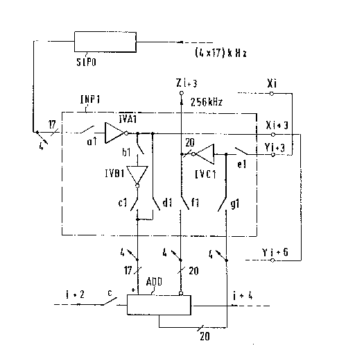
Fig. 1 shows the essenti~l elements oF the new
multiPlex interpolator which c~n be used in a Digital
Signal Processor of the gener~l tyPe dlsclosed in the above
5 article concerning a digital codec ~nd more particularlY in
the receive path of such a PCM telePhone line circuit. As
noted above, in this earlier realisatlon using a 3 ~icron
CMOS technology, after a first interPolation from 8 to 3Z
kHz that from 3Z to Z56 kHz was based on the use of binarY
10 dividers now avoided bY the new design usable in a l.Z
micron technology and in multiplex manner for 4 speech
channels instead of for a single subscriber line circuit as
in the above article. In ffie new design the digit~l hy~rid
linklng the receive to the transmit Path and designed to
15 cancel under software control the excess echo return signal
that Passes through the analoD hybrid, was fed by the 3Z
kHz signals and with the 4 ch~nnels now being multiPlexed,
the 3Z to 256 kHz interpolation in the receive Path again
takes Place after the digital hYbrid derivation. The
Z0 interpol~tion from 8 to 32 kHz c~n, as in the above
European patent aPPlication, transform the i3-bit into
17-bit words and ~pPly them to the DC blocking circuit
disclosed by th~t application and which is designed to
output the words still in the 17-bit format and ~t 32 kHz
25 but without a DC error comPonent due to noise. As
disclosed in that ~pplic~tion this Processing relies on the
use of ~ rounding bit ~s the 17th LSB fr~ction~l P~rt which
is ~dded to the integral P~rt of the word constituted by 15
bits, I.e. all the remaininD ones eXcePt the MSB
30 constituting the sign bit. It maY thus be ~ssumed th~t
17-bit words are to be interPolated from 32 to 256 kHz ~s
before but this time in multiPlex f~shion for 4 independent
ch~nnels.
Fig. 1 represent5 ~n inPUt seri~l to parallel
35 converter SIP0 with its inPut fed bY ~ serial stre~m of
' 1.
. 1'
72430-159 I Y
,~ 2~51583
. .
-- 9 --
bits at 4x3Zx32 kHz the indication of of 4x17 on Fig. 1
reflecting thc fact that onlY 17 out of 32x32 bits are
useful ones. This Serial In Parallel Out converter
Produces Parallel outputs on 17 conductors, as indicated by
5 the slash reference on the single conductor shown, with the
serial stream on each of the 17 conductors now being at
4x32=128 kHz The 17 bits of each word are thus processed in
Parallel using a bit slice structure with the LSB entering
the SIP0 first and with such a technologY as 1.2 micron
10 CMOS imPlYing sufficiently fast CarrY proPagation between
'~ adder stages. For each of the 17 bit "planes", Fig. 1
shows that each of the 17 conductors feeds 4 identical
circuits in Parallel, as indicated by the multiPling arrow,
with only the first (INPI~ shown in detail and comPrising
15 various gates such as al, represented by open contacts, and
logic inverters, used for bit storage on their inPut
capacitance, such as IVAl. The four circuits such as INP1
are intercoupled with a Parallel ~dder~subtractor ADD with
one stage thereo ~ associated with a corresponding bit Plane
20 out of the 17 so that inPut/outPut CarrY connections extend
between these planes starting from the LSB. Subtraction is
carried out on a two's complement obasis.
With the circuits of Fig. 1 having to process 4
independent words at 32 kHz in multiPlex fashion the -
25 various gates such as al in INPl are oPerated duringpredetermined time slots which are rePeated in cYcles of
128 consecutive time slots within a Period of 1000~32=31.25
microseconds so that 4 words can be simultaneouslY and
indePendently processed at the interPolator inPUt rate of
30 32 kHz while delivering 4 indePendent output words at
8x32=256 kHz.
Fig. 2 shows pulse waveforms defining these 128 time
slots in a period of 31.25 microsecond and which are
Provided bY a 7-stage binarY counter (not shown) driven by
35 clock pulses at 128x32=4096 kHz, and which maY be reset
2~ g3
-- 10 --
Periodic~lly t~ avoid loss of synchronism with other
circuits ~not shown ), so that the first stage of the
counter produces the shown complementarY square waveforms A
and A having a Period equal to twice that (244 nanosecond~
5 of the driving clock Pulses. In turn, the second stage
outputs the B and B square waveforms at 4 times the input
Period and so on until ttle 7th stage ProduCing the G and G
square wavefor~s at a Period of 31.25 microsecond. These 7
Pairs of comPlementary binarY pulse waveforms thus define
n lZ8 time slots of 244 nanosecond such as O during which A,
B, C, D, E, F, G are simultaneouslY ON and lZ7 when this is
true for A, B, C, D, E, F, G.
These various pulses are used to control the gates
of Fig. I with the help of a Z-Phase clock sYstem at the
15 4U96 kHz rate so that such u and v non-overlaPPing strobe
Pulses tnot shpwn) reaPPear everY 244 nanosecond, with u
preceding v.
Fig. 3 shows a table linking the various control
pulses to the Yarious gates. The Pulses are associated to
20 the binarY counter waveforms used to define the time slots
and to u or v followed by a number from O to 127
corresponding to the time slots of Fig. 2. The gates
reference letters are associated to their resPective
interpolator circuit INPl, 2, 3 or 4 of which only the
2S first is shown in detail in Fig. 1. Thus, the table has 4
rows corresponding to these 4 interPolator circuits and 6
columns onlY for the gates a, b~e, c, d, f, g since b ~nd e
are oPerated in sYnchronism.
Jointly referring to Figs. 1 to 3, it is now seen
30 that the a and b gates, e.g. al and bl in INPl, are only
conductive ~closed contact3 ~t the beginning of each
distinct quarter Period of 3Z time slots in order that the
a gates should latch the new incoming words Sitl into IAV
(input shunt capacitance) while the Si words PreviouslY
35 stored therein are shifted into IVB through the b gates,
_ _ , , _ , _ _ _ _ _ _ _ _ _
- ~ 20~ ~ 583
this implying that the u strobe pulses are used for the
latter step, i e before the v strobe pulse~ gate in Si+l
Thus, Figs 2 ~nd 3 indic~te that al, Z, 3, 4 are ON during
the occurence of VOt 32~ 64, 96 and bl, Z, 3, 4 during uO,
5 32. 64, 96 respectively! After a full period of 128 time
slots ~nd equ~l to 31 25 micro~econd the next word will be
~vail~ble from SIPO
Simult~neously With the shift of Si into IVB through
b, it will ~lso be shifted through e into IVC u~ed ~
10 ~ccumul~tor for ADD, the l~tter ~cting in multiPlex for
INPl 2~ 3 4 ~5 lndic~ted by the 4 multiPllng ~rrow Thus,
~5 confirmed bY Fig 3, b ~nd e are oPer~ted in
5Ynchronism~ Indeed, ~s shown bY Fig 1, the lo~ding of Si
from IYA into IVC occurs with ~ shift of 3 bits in such ~
15 way that actuallY 8 Si is stored in'co IVC, ouput terminal
Xi+3 of IVA for the shown bit plane i+3 being connected to
input terminal Yi+6 of IYB for bit pl~ne i~6 while Al in
bit Pl~ne i is connected to ~i+3
The 4 series of input words , Si, Si+l,
20 having thus been shown to be fed from SIP~ into IYAl, 2, 3.
4 in st~ggered fashion on a continuous basis. the function
of the rem~inin9 9~tes c, d, f ~nd o will now be expl~ined
in connection with the Processing of Si+l l~tched into IVA,
Si into IVB and 8Si lnto IY~ in order to successivelY
25 output in multiplex the 4 series rf interPol-ted words 7Si
Si+l, 6Si ~ 2 Si+l, . , Si+7Si~l. 85i+1 All these 4
rem~inino tyPe~ of ~te~ ~r~ ~g~in ~ch u~ino mutu-llY
exclusive time slots out of the 128 depending in which of
INPl, 2, 3 or 4 such g~tes as c, d. f ~nd 9 rlt loc~ted
30 But where~s the st~rt of successive qu~rter Periods of 32
time slots is used in connection with g~te~ ~, b ~nd e.
groups of 4 consecutive time slots ~re successivelY
~ssigned to g~tes c, d, f and 9 in INPl, 2. 3 ~nd 4, this
being continuously rePe~ted so th~t such g~tes c~n be
35 oPerative 8 times during ~ Period of 128 slo~s in order to
~ .
~J ~
:
20~ 3
-- 12 --
output 8 interpolated words at Z56 kHz. Thus 128~8=16
consecutive time slots would in princiPle be available for
each of the 4 words interPolated in multiPlex, i.e. 16/4=4
for each outPut word.
The gates f and g link the accumul~tor IVC to the
adder~subtractor ADD, the l~tter used in multiPlex. f from
the output of IVC to the inverted inPut of ADD and g from
the sum outPut of ADD to ~VC.
As shown by Fig. 2 and 3, fl is ON during the
10 occurrence of u2, 3, 18, 19, .. , 98, 99, 114, 115 since
IVCl must first be unloaded before a new word is latched
therein from ADD, although both qates are successivelY
operated bY the non-overlaPPing u and v strobe Pulses
during the same indicated 16 time slots 2, 3, 18, 19, ....
98, 99, 114, 115. The table of Fig. 3 indicates the 3
other series of 16 time slots involved for INP2, 3 and 4,
i.e. for gates f/g2, 3 and 4
The gates c and d link the positive inPut of ADD to
either the outPu~ of IVB or IVA resPectivelY, i.e. to admit
20 either the PreYious -Si or the new Si+l inPut word.
The sign of the latter is reversed with respect to
Si, as required for the incrementation bY the difference
between the two, in view of a double logic inversion when
passing 2's complement format (MSB used as sign bit, i.e. 0
25 for Positive ~nd 1 for negative, and 1 's complement, i.e.
inversion, becoming 2's complement bY a +l LSB carrY input~
words through IVA and IVB in cascade as opPosed to one
inversion through IVA only. C~rrYing out the subtraction
of Si+l before the ~ddition of Si means that no overflow
30 circuitry is needed.
As shown by Figs. 2 and 3, cl is ON during the
occurence of u2, 18, 34, 50, 66, 82, 98, 114 and dl durins
u3, 19, 35, 51, 67, 83, 99, 115 and again, the use of such
8 successive pairs of consecutive time slots, e.g. 2 ~nd 3,
35 is also the case for the 3 other series of u pulses
_ _
2~
. . _
-- 13 --
associated with c/d2, 3, 4 in INP 2, 3, 4 resPectivelY and
identified in the table of Fig. 3.
Together with the binarY pulse waveforms of Fig. 2,
the table shows that 16 consecutive time slots can cYcle
5 the C and D stages of the binary counter ~not shown~,
defining the time slots, exactlY through their 4 Possible
conditions with each of the 4 associ~ted with one out of
INPl, 2, 3 or 4, e.g. DD for INPl. But the 16 time slots,
or 4 Per word, are not all avail~ble for the operations
10 needed to produce the 4 new interpolated outPut words since
the ~dder/subtractor ADD being used in muitiPlex for the 4
words it is necessary to initialize ADD Prior to its use in
connection with data for a different INP and this is
achieved by using onlY half these available time slots,
15 i.e. those associated with B.
On the other hand, those associ~ted with B can
conveniently be used for insertion of the new words through
- the a, b and e gates without anY interference with the
oPerations invol--ing ADD since Fig . 3 shows that these gates
2D are all controlled during B and not B time slots.
Thus, considering INPl, during time slot 2, u strobe
pulses render gates cl and fl conductive so that ADD will
compute the difference between 85i ~nd Si to produce ~Si.
This takes Pl~ce in all bit Planes so that the
2~ adder~subtractor stage ADD shown in Fig. 1 for bit i+3 is
also fed with the binary carrY from the Previous i+2 stage
and this through gate c whiGh is conductive simultaneouslY
with cl, 2, 3 and 4, i.e. during time slots 2, 6, 10, 14,
18, 22, 26, 30,
.... , 114, 118, 122, 126 by controlling c onlY with AB and
not bY the C and D conditions. Such carries will aIso
include an LSB carrY inPut in order to obtain from the l's
comPlement, i.e. inversion, the 2's complement needed for
subtraction. In addition to each ADD stage delivering its
35 binary sum output through g, e.g. 91, enabled by a
_
2o5 1 ~83
-- 14 --
subsequent v strobe pulse also during time slot Z, lts
c~rry output is made available to the next i+4 st~ge To
be noted that words of Z~ bits ~re in fact suPPliQd from
and to the accumulator IVC to ~nd from ADD in view of 8Si
being stored by a shlft of 3 bits
Fig 3 indicates, ~s PreviouslY mentioned, that
gates e ~nd 9 commoned at the input of IYC cannot lead to
undesired interferences since they ~re made conductive
durlng mutuallY excluding time slots B and B and that
lD similarly this is true for gates c snd d commoned at the
input of ADD, this time due to the mutuallY excluding time
slots A and A
Hencc, considerino INPl, durlng time slot 3, the u
strobe Pulse renders gates dl and fl simultaneouslY
conductive so that ADD will now add Si~l to 7Si to comPlete
the iteration steP, a v strobe pulse during this time slot
again delivering the sum outPut from ADD through gl
After time slot 3, condition CD changes to C~ so
that INP2 can now become active in using ADD twice in the
above described manner, a complete cYcle of 128 consecutive
time slots enabling to output 4x8 interPolated words each
computed during 2 out of 4 consecutive time slots The
newly interPolated output word durlns~ time slots 2 and 3
will be ef~ect~vely ~v~ilable ~t such terminals as Zi+3 of
IVCI onlY from time slot 6 because during the intervening
time slots 4 and 5 B is 1aw The word will remain
available until the occurence of time slot 16 and likewise
for all words 50 that there c~n be no interference with a
new inPut word being fed into IVCl during time slot 0
This means that the 20-bit output words ~re
avail~ble for further processing during ID successive time
slots out of a theoretic31 maximum of 16 During such time
intervals, these demultiplexed 256 kHz outPut words c-n be
transmitted to corresponding digital sigma-delta modulators
such as disclosed ln the ~bove EuroPe~n patent aPPlic-tion
!
72430-15g
2051~83
. .
-- 15 --
Therein, the digital words can be further interPolated to
l-bit words at lQ24 kHz.
While the PrinciPles of the invention have been
described above in connection with speciflc aPParatus~ it
5 is to be clearlY understood that this description is made
only by waY of examPle and not as a limitation on the scoPe
o~ the inv~ntion.