Language selection

Search

Patent 2052031 Summary

Third-party information liability

Some of the information on this Web page has been provided by external sources. The Government of Canada is not responsible for the accuracy, reliability or currency of the information supplied by external sources. Users wishing to rely upon this information should consult directly with the source of the information. Content provided by external sources is not subject to official languages, privacy and accessibility requirements.

Claims and Abstract availability

Any discrepancies in the text and image of the Claims and Abstract are due to differing posting times. Text of the Claims and Abstract are posted:

  • At the time the application is open to public inspection;
  • At the time of issue of the patent (grant).
(12) Patent: (11) CA 2052031
(54) English Title: CHARGING CIRCUIT FOR RADAR TRANSMITTER
(54) French Title: CIRCUIT DE CHARGE POUR EMETTEUR RADAR
Status: Expired and beyond the Period of Reversal
Bibliographic Data
(51) International Patent Classification (IPC):
  • H03K 03/53 (2006.01)
  • H02M 03/158 (2006.01)
(72) Inventors :
  • STEGEMAN, ALBERT PIETER
(73) Owners :
  • HOLLANDSE SIGNAALAPPARATEN B.V.
(71) Applicants :
  • HOLLANDSE SIGNAALAPPARATEN B.V.
(74) Agent: SMART & BIGGAR LP
(74) Associate agent:
(45) Issued: 1999-03-16
(22) Filed Date: 1991-09-23
(41) Open to Public Inspection: 1992-04-05
Examination requested: 1996-07-09
Availability of licence: N/A
Dedicated to the Public: N/A
(25) Language of filing: English

Patent Cooperation Treaty (PCT): No

(30) Application Priority Data:
Application No. Country/Territory Date
9002153 (Netherlands (Kingdom of the)) 1990-10-04

Abstracts

English Abstract


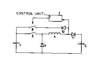
An improved resonant charging circuit is disclosed for the charging
of a pulse-forming network (5) from a voltage source (1), provided
with:
i) a first serial circuit provided with a switch (3), an
inductor (4), and a diode (11);
ii) a second serial circuit provided with a diode (6), the
inductor (4), a diode (10), and a switch (8);
iii) a control unit (2) for opening and closing the switches (3, 8).


French Abstract

Circuit de charge résonant amélioré permettant la charge d'une ligne à retard (5) depuis une source de tension (1), comprenant les éléments suivants : i) un premier circuit en série muni d'un commutateur (3), d'une bobine d'inductance (4) et d'une diode (11); ii) un deuxième circuit en série comprenant une diode (6), une bobine d'inductance (4), une diode (10) et un commutateur (8); iii) une unité de commande (2) pour ouvrir et fermer les commutateurs (3, 8).

Claims

Note: Claims are shown in the official language in which they were submitted.


THE EMBODIMENTS OF THE INVENTION IN WHICH AN EXCLUSIVE
PROPERTY OR PRIVILEGE IS CLAIMED ARE DEFINED AS FOLLOWS:
1. A changing circuit for charging, from a voltage
source, a pulse-forming network to a predetermined voltage,
comprising:
a first serial circuit provided with a first
switching element, an inductor, a first diode and the
pulse-forming network;
a second serial circuit provided with a second
diode, the inductor, a third diode and a second switching
element; and
a control unit for opening and closing the first and
second switching elements, whereby the control unit closes the
first switching element at the start of a charging cycle, for
causing the energy from the voltage source to be supplied to
the pulse-forming network via the first serial circuit and
whereby the control unit opens the first switching element
when the predetermined voltage has been reached and
substantially simultaneously closes the second switching
element for causing the energy contained in the inductor to
flow back to the voltage source.
2. The circuit as claimed in claim 1, wherein the first
and second switch are provided with Insulated Gate Bipolar
Transistors.
-6-

Description

Note: Descriptions are shown in the official language in which they were submitted.


3 ~ -'
Charqlnq clrcult for radar transmltter
The invention relates to a charging circuit for charging, from a
voltage source, a pulse-forming network to a predetermined voltage.
Such a circuit can be applied in a radar transmitter for the
generation of radar transmit pulses. The radar transmitter will in
that case be provided with a high-power radar transmitter tube, such
as a crossfield amplifier, a travelling wave tube or a klystron,
whose cathode must be brought to a pulsed high voltage. The
high-voltage pulses are generated by a high-voltage transformer, the
primary winding of which is connected to a low-voltage pulse
generator, consisting of at least a pulse-forming network and a
switching element.
As regards applications where a radar system's only task is to
detect moving objects, heavy demands are made on the reproducibility
of the high-voltage pulses, applied to the radar transmitter tube.
As a consequence of minor variations in the high-voltage pulses,
stationary objects also seem to move, which may easily cause an
overload on the equipment, processing the target echoes, received
by the radar system.
The reproducibility of the high-voltage pulses is to a considerable
extent determined by the reproducibility of the charging voltage of
the pulse-forming network. The charge is usually provided by a
buffer capacitor, which is powered from the mains via a rectifier
circuit.
The charging voltage of the buffer capacitor is not constant, it
varies with the mains voltage and is often afflicted with a ripple
voltage, originating from the rectifier circuit.
24005-180

~ ~ ~ 2 ~
A method well-known ln the art for charglng a pulse-
forming network is the resonant charging through an inductor.
If the pulse-forming network has reached the required voltage,
the charging current is lnterrupted and the residual energy
stored in the inductor is fed back via a clrcult whlch ls
connected to the inductor by way of secondary winding. At
that moment the lnductor ls ln fact a transformer.
The drawback of thls method ls that the resldual
energy ln one wlndlng of a transformer can never be completely
dralned vla the other wlndlng of that transformer, because of
the leakage self-lnductance of the transformer. As a
consequence, the pulse-formlng network wlll recelve some
addltional charge from the prlmary wlndlng of the transformer
after the lnterruptlon of the actual charglng current.
Moreover, the amount of addltional charge is a function of the
lnstantaneous charging voltage of the buffer capacltor, which
means that the reproducibility of the charging voltage of the
pulse-forming network is adversely affected.
The lnvention elimlnates thls drawback and is to
this effect provided with: a first serial circuit provlded
wlth a flrst swltchlng element, an inductor, a first diode and
the pulse-formlng network; a second serlal circuit provided
wlth a second diode, the inductor, a third diode and a second
switching element; and a control unit for opening and closing
the first and second switching elements, whereby the control
unit closes the first switching element at the start of a
charging cycle, for causing the energy from the voltage source
to be supplied to the pulse-forming network via the flrst
24005-180

serlal clrcult and whereby the control unlt opens the flrst
swltchlng element when the predetermlned voltage has been
reached and substantlally slmultaneously closes the second
switchlng element for causing the energy contained ln the
inductor to flow back to the voltage source.
- 2a -
24005-180

20~2~31.
The invention will now be described in more detail with reference to
the following figures, of which:
Fig. 1 illustrates a simple resonant charging circuit;
Fig. 2 illustrates a state-of-the-art charging circuit; and
Fig. 3 illustrates a charging circuit according to the invention.
A simple circuit of the resonant type is schematically represented
in Fig. 1. A buffer capacitor 1 is charged from the mains voltage.
Under the control of a control unit 2, switching element 3 closes,
as a result of which current can flow via an inductor 4 to a
pulse-forming network 5, in this case represented by a capacitor.
In reality, pulse-forming network 5 is also provided with inductors,
but these hardly play any role during charging. The voltage on the
pulse-forming network 5 is applied to control unit 2 and when this
voltage has reached a predetermined value V, switching element 3 is
opened under the control of control unit 2. At this moment there
will still be a current I flowing through inductor 4. Via a diode 6
this current can continue to flow after the opening of switching
element 3. Eventually the current will cease to flow, but the
voltage on the pulse-forming network has meanwhile increased
according to the formula:
~ C(V')2 = ~C v2 + ~L I2
where C is the capacitance of the pulse-forming network 5, L is the
self-inductance of inductor 4, V is the voltage on the pulse-forming
network during the opening of switching element 3, I is the current
through the inductor 4 during the opening of switching element 3 and
V' is the ultimate voltage on the pulse-forming network; this on the
assumption that the capacitance of buffer capacitor 1 is very much
larger than the capacitance of pulse-forming network 5.
The ultimate voltage V' depends on I and consequently on the
instantaneous voltage on buffer capacitor 1. This voltage in
particular strongly fluctuates, as a consequence of mains
fluctuations and a continuously present ripple voltage, caused by
the rectification of the mains voltage.

~052Q3~.
A state-of-the-art charging circuit of the resonant type is
represented in Fig. 2. Here again, switching element 3 closes under
the control of the control unit 2, as a result of which a current
can flow to pulse-forming network 5 via a primary winding 7A of a
transformer 7. A switching element 8 is in open condition, so that
no current can flow in a secondary winding 7B of transformer 7. In
this condition the primary winding of transformer 7 actually forms
an inductor, so that the behaviour of the circuit is identical to
that of the circuit which is schematically represented in Fig. 1.
When the voltage on pulse-forming network 5 has reached a
predetermined value V, switching element 3 is opened under the
control of control unit 2. At the same time, however, switching
element 8 is closed, as a result of which energy, stored in the
magnetic field of transformer 7, is fed back to buffer capacitor 1
via a current through the secondary winding, a diode 9 and switching
element 8. If the magnetic coupling between the primary winding 7A
and the secondary winding 7B of transformer 7 is perfect, the
condition can be attained that no more energy is supplied to
pulse-forming network 5 after the opening of switching element 3. In~0 the event of a less perfect coupling the following applies again:
~C(V')2 = ~C v2 + ~L I2
L now representing however the leakage self-inductance of
transformer 7. As compared with the simple charging circuit, as
schematically represented in Fig. 1, there is an improvement of
orders of magnitude in the reproducibility of the charging voltage
of the pulse-forming network.
A charging circuit according to the invention is schematically
represented in Fig. 3. Switching element 3 closes again under the
control of control unit 2, as a result of which current can flow to
pulse-forming network 5. Switching element 8 is in open condition.
When the voltage on pulse-forming network 5 has reached a
predetermined value V, switching element 3 is opened under the
control of control unit 2. At the same time switching element 8 is

~ ~ $ ~
closed however. ~he current I, whlch at that moment stlll
flows through lnductor 4, wlll be fed back to the buffer
capacltor 1 vla dlode 6 and dlode 10.
A precondltlon ls that, at the openlng of swltchlng
element 3, the voltage on pulse-forming network 5 exceeds the
voltage on buffer capacltor 1. Slnce the capacltance of
buffer capacltor 1 ls much larger than the capacltance of
pulse-forming network 5, the voltage on pulse-formlng network
5 wlll, when switching element 3 does not open, eventually be
virtually twice the voltage on buffer capacitor 1 as a result
of the resonant charging, so that the above precondition can
always be met.
In implementing the charging circuit as
schematlcally represented in Flg. 3, Insulated Gate Blpolar
Transistors may be used to advantage as switching elements,
which transistors, even with the large currents in the
charging circult they have to cope wlth, stlll achleve a short
swltchlng tlme.
24005-180

Representative Drawing
A single figure which represents the drawing illustrating the invention.
Administrative Status

2024-08-01:As part of the Next Generation Patents (NGP) transition, the Canadian Patents Database (CPD) now contains a more detailed Event History, which replicates the Event Log of our new back-office solution.

Please note that "Inactive:" events refers to events no longer in use in our new back-office solution.

For a clearer understanding of the status of the application/patent presented on this page, the site Disclaimer , as well as the definitions for Patent , Event History , Maintenance Fee  and Payment History  should be consulted.

Event History

Description Date
Inactive: IPC from MCD 2006-03-11
Time Limit for Reversal Expired 2001-09-24
Letter Sent 2000-09-25
Grant by Issuance 1999-03-16
Inactive: Final fee received 1998-11-25
Pre-grant 1998-11-25
Notice of Allowance is Issued 1998-10-15
Letter Sent 1998-10-15
Inactive: Application prosecuted on TS as of Log entry date 1998-10-09
Inactive: Status info is complete as of Log entry date 1998-10-09
Inactive: First IPC assigned 1998-09-10
Inactive: IPC removed 1998-09-10
Inactive: IPC assigned 1998-09-10
Inactive: Approved for allowance (AFA) 1998-09-09
Request for Examination Requirements Determined Compliant 1996-07-09
All Requirements for Examination Determined Compliant 1996-07-09
Application Published (Open to Public Inspection) 1992-04-05

Abandonment History

There is no abandonment history.

Maintenance Fee

The last payment was received on 1998-06-16

Note : If the full payment has not been received on or before the date indicated, a further fee may be required which may be one of the following

  • the reinstatement fee;
  • the late payment fee; or
  • additional fee to reverse deemed expiry.

Patent fees are adjusted on the 1st of January every year. The amounts above are the current amounts if received by December 31 of the current year.
Please refer to the CIPO Patent Fees web page to see all current fee amounts.

Fee History

Fee Type Anniversary Year Due Date Paid Date
MF (application, 6th anniv.) - standard 06 1997-09-23 1997-06-26
MF (application, 7th anniv.) - standard 07 1998-09-23 1998-06-16
Final fee - standard 1998-11-25
MF (patent, 8th anniv.) - standard 1999-09-23 1999-06-22
Owners on Record

Note: Records showing the ownership history in alphabetical order.

Current Owners on Record
HOLLANDSE SIGNAALAPPARATEN B.V.
Past Owners on Record
ALBERT PIETER STEGEMAN
Past Owners that do not appear in the "Owners on Record" listing will appear in other documentation within the application.
Documents

To view selected files, please enter reCAPTCHA code :


To view images, click a link in the Document Description column. To download the documents, select one or more checkboxes in the first column and then click the "Download Selected in PDF format (Zip Archive)" or the "Download Selected as Single PDF" button.

List of published and non-published patent-specific documents on the CPD .

If you have any difficulty accessing content, you can call the Client Service Centre at 1-866-997-1936 or send them an e-mail at CIPO Client Service Centre.


Document
Description 
Date
(yyyy-mm-dd) 
Number of pages   Size of Image (KB) 
Abstract 1994-04-15 1 9
Drawings 1994-04-15 1 16
Description 1994-04-15 5 164
Claims 1994-04-15 1 26
Description 1998-08-11 6 204
Claims 1998-08-11 1 34
Drawings 1998-08-11 1 15
Representative drawing 1999-03-09 1 3
Commissioner's Notice - Application Found Allowable 1998-10-14 1 164
Maintenance Fee Notice 2000-10-22 1 178
Correspondence 1998-11-24 1 37
Fees 1996-06-11 1 47
Fees 1995-06-21 1 45
Fees 1994-06-16 1 41
Fees 1993-06-20 1 29
Prosecution correspondence 1996-07-08 1 43
Courtesy - Office Letter 1996-07-08 1 42
Examiner Requisition 1997-02-13 1 49
Prosecution correspondence 1997-05-07 3 62