Note: Descriptions are shown in the official language in which they were submitted.
The present invention relates to a connector device
for connecting, for example, printed circuit boards to
each other.
This invention can be more fully understood from the
following detailed description when taken in conjunction
with the accompanying drawings, in which:
Fig. l is a perspective view showing a conventional
connector device;
Fig. 2 is a cross-sectional view showing the
connector device shown in Fig. 1;
Fig. 3 is a partly-explodedl perspective view showing
latching metal members and housing of a connector device
according to one embodiment o~ the present invention;
Fig. 4 is a perspective view showing part of the
connector device with the latching metal members arranged
in the housing in the embodiment shown in Fig. 3;
Fig. 5 is a perspective view showing the latching
metal member shown in Fig. 3; and
Fig. 6 is a cross-sectional view showing the latch
member and the latch member holding section shown in Fig.
4.
A connector device 50 as shown, for example, in Fig.
1 is known as a connector device for making an electrical
;~ 25 connection between, for example, printed circuit boards.
The connector device 50 is used to electrically connect a
first circuit board 53 to a second circuit board 63 and
~`:
- 2 -- 3 '`' ' 2 ~ ~ ~
has a housing 51 made of plastics. The firsk circuit
board 53 is diagonally inserted into a groove 52 of the
housing 51 and swung, in a direction as indicated by an
arrow 54, to an upright position as shown in Fig. 2. The
upright circuit board 53 makes electrical contact with
connection terminals 55 by being sandwiched by spring
force of the connection terminals 55 held in a groove. A
pair of latching sections 56, 57 are provided on both the
end portions of the housing 51 to securely hold the
circuit board in the upright position. During the
swinging of the circuit board 53, the latching sections 56
and 57 are pushed, while being elastically flexed
outwardly of the housing, away from each oth~r by the
circuit board 53 and, upon the reaching the upright
position, returned back to an original position, thus
holding end surfaces 58 and 59 of the circuit board 53
therebetween. A the same time, those mutually facing
faces 60 and 61 of projections o~ the latching sections 56
and S7 ~upport a surface 62 oE the circuit board, holding
the circuit board 53 to the upright position. Upon the
detachment of the circuit board 53 from the connector
device 50, the latching sections 56 and 57 are pushed and
outwardly ~lexed, away from each other, removing the
circuit board 53 from the connector device. The latching
sections 56 and 57 are made of plastics and formed
integral with th housing 51.
:
~: ~
:
~ 3
However, the plastics latching sections 56 and 57
used in the conventional connector device are liable to
crack, break, etc., failing to impart any adequate
withstand property to the connector device. Further, upon
the repeated attachment and detachment of the circuit
board to and from the connector device, the latching
sections are not returned back to the original position
and the board holding force o the latching sections is
decreased, enabling no adequate electrical connection to
be made between the circuit board ~nd the connection
terminals. The latching sections are also liable to be
damaged or worn out due to a frictional force involved
upon the attachment and detachment of the circuit board to
and from the connector device. It is difficult to
manufacture the latching sections of complex shape such
that they are formed integral with the housing with the
; use of plastics. High accuracy is required upon the
manufacture of such complex latching sections. Due to the
limited flexibility of the plastics, a considerable force
is also required when the latching sections are pushed
away from each other upon the attachment and detachment of
the ixcuit board.
It is accordingly the object of the present invention
to provide a connector device having a readily
; manufactureable latching means of longer durability.
~ According to the present invention, there is provided
t~
~ 4
a connector device comprising: a housing made of an
insulating material, which has a groove including
connection terminals for coming into electrical contact
with a row array of connection terminals of a first
circuit board and inserted therein and with second circuit
board, the first circuit board begin partially housed in
the groove; latching means having a pair of metal strips
mutually oppositely provided one at each end of the
housing at an interval corresponding to a length of the
first circuit board in a direction in which the connection
termina:Ls are arranged as the row array, the pair of me-tal
strips elas~ically holding the partially inserted first
circuit board therebetween under an elastic force acting
in a direction perpendicular to that in which the
connection terminals of the first circuit board are
arranged as the row array; holding means for holding the
latching means relative to the housing; and fixing means
for positionally fixing the first circuit board, which is
held by the latching meansl relative to the housing in a
direction of the thickness of the first circuit board.
The connector device of the present invention
utilizes metal strips, as a latching means, in place of
: conventionally employed latching sections made of
plastics. The use of such metal strips ensures remarkably
durable latching sections and can maintain their stable
and strong holding power even in the event of the repeated
.
,
~ . .
I~J ''`. ~ C~
-- 5
attachment and detachment of the metal strips to and from
the connector device. In the connector device of ~he
present invention, it is possible to ready replace damaged
metal strips with new ones. Further, since the metal
strips are provided separate from the housing and
replaceable as separate members, the accuracy with which
the housing is formed is alleviated, ensuring ready
manufacture of the housing~
A connector device according to one embodiment of the
present invention will be explained below with reference
to the accompanying drawings.
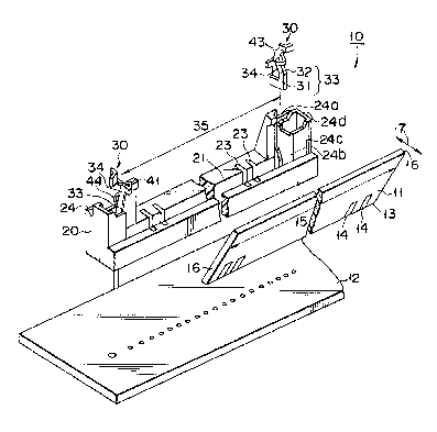
Fig. 3 is a perspective, exploded view showing a
connector device lO according to the embodiment of the
present invention. The first circuit board 11 is inserted
in, and mounted on, the connector device lO to
electrically connect itself to the second circuit board by
the connector device.
The connector device 10 includes a housing 20 made of
an insulating material, such as plastics. The housing 20
has a longitudinally extending groove 21 where a plurality
of connection terminals 23 are provided at given intervals
along the length of the groove such that they are arranged
as a row arrayO A plurality of connection terminals 14
2S are arranged, as a row array~ along a side edge portion 13
of the ~irst circuit board 11, come into elastic contact
with and electrically connected to the corresponding
connection terminals 23
J ~
at the groove 21 of the housing. It is possible to
use, as connection terminals 23, any proper elastic
connection terminals for the connection of a printed
circuit board or a circuit board such as a single-in-
line modulator (SII,M). The connection terminals 23 ofthe housing is electrically connected to the second
circuit 12 by any proper method for, for example,
inserting the connection terminals into corresponding
through holes provided in the second circuit board 12.
The connector device of the present invention has
latching means at both the end portions of the housing
so as to hold the ~irst circuit board, which is inserted
in the groove of the housing, in a position where the
connection terminals of the ~:irst circuit board are
electrically connected to the connection terminals pro-
vided in the groove of the housing.
The connector device of the present invention has
pair of latching members 30 made of a metal and having a
mirror image relation to each other as shown in Fig. 3.
The latch member 30 is formed by, for example, stamping
out an elastic metal plate, such as phosphor bronze.
As shown in Figs. 4 and 5, the latching member 30
has a strip portion 33 including a support beam 31 and a
spring beam 32 ex~ending from one end of the support
beam 31.
As shown in Fig. 3, a pair of strip portions 33 are
disposed at a distance corresponding to a length the
~3 ~
first circuit board in a direction of the array of con-
nection terminals such that they face each other. It is
necessary that a spacing 35 defined by the mutually
opposite faces 34 and 3~ at the free end portions of the
respective spring beams 32 and 32 be made somewhat
narrower than the aforementioned length 15 so that the
first circuit board 11 may be elastically held between
the strip portions 33 and 33 by those elastic forces
of the spring beams of the strip portions acting in a
direction perpendicular to that in which the connection
terminals of the first circuit board 11 are arranged as
the row array with the side edge portion 13 of the first
circuit board fitted in the groove 21 of the housing and
held in elastic contact with the connection terminals,
that is, in a direction perpendicular to a plane corres-
ponding to a side face 16 as shown in Fig. 3. In the
present embodiment, the spring beam 32 of the latrhing
member 30 is obtained, by bending the strip from the
support beam at a given angle, which provides a desired
holding power at a narrowed spacing between those faces
34 and 34 at the free end portions of the spring beams
of the respective strip portions 33 and 33. In the
connector device of the present invention it is pre-
ferable that the metal strips o~ the latching means,
each, include a spring beam adapted to make elastic
contact with the first circuit board and a support beam
adapted to support the base end of the spring beam and
3 2 ~
-- 8
that the spring and support beams be obtained b~ bending
a single metal sheet.
The connector device of the present invention
includes holding means for holding the latching means
wi-th respect to the housing.
The connector device of the present invention in~
cludes, as the holding means, a pair of holding beams 36
and 36, each, formed on an extension of the support beam
31 of the latching member 30 and a pair of latching
member holdiny sections 24 provided on both the ends of
the housing 20. The holding beam 36 has a pair of
holding tabs 37 and 38 on its upper and lower ends and
two dimples 39, 39 between the tabs. The latching
member holding section 24 of the housing is of such a
type that the latching member 30 is fixed to the housing
20 with the holding tabs 37 and 38 engaged to the
latching member holding section. The latching member 30
is more positively fixed to the housing 20 through the
frictional contact of the rear portion of the dimple 39
of the holding beam 36 of the latching member 30 with
the inner surface of a first wall section 24a of the
latching member holding section 24. The cross-sectional
view of the latch member holding section 24 is shown in
Fig. 6.
It is preferable that the spring beam 32 of the
latching member 30 be abutted against the i.~ner surface
of a second wall 24b of the latching member holding
section 24 of the housiny 20. By so doing, frlctional
contact is provided between the spring beam 32 of -the
strip and the second wall 24b so that the latching
member 30 can be positively fixed to the housing 20 in
the longitudinal direction of the housing 20. Further,
a side surface 31a of the support beam 31 an~ side
surface 32a of the spring beam of the latching member 30
lie on the same plane and the side surface 32a of th~
spring beam 32 of the latching member 30 is in contact
with the inner surface or a third wall 24c of the
latching member holding section 24.
A fixing means for fixing the first circuit board
whlch is held by the latching means in the connector
device of the present invention to th0 housing in a
direction of the thickness of the first circuit board
will be explainPd below. With the first circuit board
inserted in the groove of the housing and held there by
the latching means, the first circuit board is pressed
in the direction of its thickness by the elastic forces
of all the connection -terminals at the groove of the
housing. It is, therefore, necessary to provide a
fixing means for fixing the circuit board to its proper
position against the elastic pressing forces of the
connection terminals at the groove of the housing.
The connector device 10 of the present invention
includes a fixing section 40 provided on the latching
member 30 as the fixing means. The fixing section 40
,~, ...' ~ ('J ~V ..~. ~J
-- 10 --
includes a bent band-like section 45 extending from the
side edge of the spring beam 32. As shown in Fig. 3,
the paired latching rnembers 30, 30 have the fixing sur-
faces 41 of their fi~ing sections lay on the same plane.
Since, as set out above, the side surface 32a of the
spring member 32 of the latching member 30 is held in
contact with the third wall 24c of the latching member
holding section 24, the fixing surface 41 of the fixing
section 40 of the latching member 30 can support the
circuit board 11, which is held in elastic contact with
the connected terminals 23, against the elastic pressing
~ force of the contact terminal 23 and, hence, the circuit
: board 11 is fixed to the housing 10 in the direction of
its thickness as indicated by arrows, in Fig. 3, 17.
In the connector device of the present invention,
as shown in Figs. 3 to 6, the band-like section 45 of
the fixing section 40 of the latching metal member is
preferably provided as a triangularly bent section and
extends from an outer to an inner direction of the hous-
ing with the fixing surface 41 provided at the forward
end of the surface 42 of the band-like section 45. By
so doing, the surfaces ~2 of the band-like sections 45
guide the first circuit board inserted in the groove of
the housing, as will be later described in connection
with the swinging motion of the first circuit board, and
; can displace the metal strip in a direction opposite to
a direction of its elastic displacement for holding the
J ;~ ~`J 2 ~ r ~
~ 11 -
circuit board between the latching members.
Upon the mounting of the first circuit board 11 on
the connection device 10 as set out above, the circuit
board 11 is diagonally inserted in the groove 21 of the
housing 20 with its side edge 13 down, noting that the
side edge portion of the circuit board 11 has the connec-
tion terminals as an array. Upon the swinging of the
circuit board with the side edge 13 of the circuit board
11 inserted in the groove of the housing, the side face
16 of the circuit board 11 slides on the guide surface
42 of the fixing section 40 of the latchiny member 30,
outwardly flexing the spring beam 32 of the elastic
member 30. When the circuit board 11 completely passes
on the guide surface, the circuit board 11 is held
b0ween the paired spring beam 32 under the latter's
elastic resil.ient forces. At the same time, the circuit
board 11 is also supported by the fixing surfaces 41 of
the fixing sections 40 of the latching members 30. In
this way, the circuit board 11 .is fixed to the housing
20, completing the mounting of the circuit board 11 to
the connector device 10.
Upon the detachment of the once mounted printed
circuit board 11 from the connector device 10, latching
release tabs 43 which are provided each at the spring
beam 32 of the latching member 30 on each end of the
housing ~0 are pushed away from each other in an outward
direction o~ the housing. When this occurs, the spring
2 ~
beams 32 are elastically flexed in the outward direction
of the housing with their areas of connection to the
support beams as ~ixed ends, releasing a holding force.
As a result, the printed circuit board 11 is pushed
outside, by the elastic pressing forces of the contact
terminals, to a pre-inserted position and can readily be
taken from the connector device. The release tabs 43
are preferably of a Z-shaped type, as in the present
embodiment, to allow the tabs to be readily pushed.
Further, it is preferable in the connector device
of the present invention to provide, on the latching
means, a structure which suppress a displacement of
the metal strips opposite in direction to the elastic
holding displacement whereby it is possible to maintain
an elastic force for holding the first circuit board
therebetween. That is, in order to prevent the spring
beams 32 from being excessively flexed in the outward
direction of the housing upon the detachment of the cir-
cuit board from the latching members, it is preferable
to provide an over-stress prevention tab 44, as in the
present embodiment, on a side opposite to that on which
the fixing section 40 of the spring beam 32 of the latch
member 30 is situated. When the elastic sections 32 are
: pushed away from each other in the outward direction of
the housing 20, the tab 44 abuts against a fourth wall
24d of the latching member holding section 2~ of ~he
housing 20 to prevent any further outward displacement
3~ 2~
- 13 -
of the spring beam 32 and hence any further fatigue of
the spring beam 32. It is, therefore, preferable to
select the length of the tab 44 to suit the object
intended.
The latching member 30, including the holding beam
36, support beam 31, spring beam 32, fixing section 40,
latching release tab 43 and over-stress prevention tab
44, is preferably formed of a single metal sheet. The
latching member 30 can be mounted on the housing 20 by
fitting it in the latching member holding section 24 of
the housing 20 made of an insulating material, such as
plastics. The latching member mounted in the latching
member holding section 24 can be readily be replaced by
a new one by ~ithdrawing it out of the latching member
holding sect.ion 24.
Although the pr~sent invention has been explained
in connection with the aforementioned embodiment, it is
not restricted to this embodiment and various changes
or modifications of the present invention can be made
without departing from the spirit and scope of the
present invention. In this example, although the
support beams 31 of the latching members 30 have been
explained as being L-shaped ones, they may take any
proper shape in so far as holding the circuit board 11
therebetween under a proper elastic force. Although
the first circuit board 11 has been explained as being
held in a position perpendicular to that of the second
i ~2~.~
- 14 -
circuit board 12, it may be held in a horizontal or
diagonal position. Further, two or more circuit boards
can be held in place by providing two or more grooves 21
in the housing 20 and providing a latching means in each
groove so as to insert two or more circuit boards.
As set out above, according to the connector device
of the present invention, the metal strips are utilized,
as the latching means, in place of the conventional
plastics latching sections, obtaining a stronger holding
power and an improved withstand characteristic. It is
also easier to manufacture them readily.