Note: Descriptions are shown in the official language in which they were submitted.
;~5~3
SPECIFICATIVI~
Tide of the Invention
SUPERCONDUCTINTG DE,VICE HAVING AN
EXTREMELY THIN SUPERCO:NDUCTING CHANNEL
FORMED OF OXIDE SUPERCONDUCTOR MATERIAL
AND METHOl:) FOR MAN~JFACTIJRING THE SAME
Background of the Invention
F~ield of the invention
The present invention relates to a superconducting de~ice and a
method for manufacturin/ the same, and more specifically to a
superconducting device having a substantially planar upper surface and
including an extremely thin superconducting channel formed of oxide
superconductor matcrial, and a method fi~ Ll~tllring ~he game.
Description of reklted art
Typical three-termina] devices which utilize a superconductor
include a so called superconducting-base transistor and a so called
super-FET (field effect transistor). The superconducting-base transistor
includes an emitter of a superconductor or a normal conductor, a tunnel
barrier of an insulator, a base of a superconductor, a semiconductor
isolator and a collector of a normal conductor, stacked in the named
order. T}'liS superconducting-base transistor operates at a high speed with
a low power consumption, by utilizing high speed electrons passing
through the tunnel barrier~
.:- :. . : .. I
,.; ~ .
. ~ . - ~, . . ..... . .
3~
The super-FET includes a semiconductor layer, and a
superconductor source eLectrode and a superconduc~or drain electrode
which ~e fol~med closely to each other on the semiconductor layer. A
portion of the semiconductor layer between the superconductor source
electrode and the superconductor drain electrode has a greatly recessed or
undercut rear surface so as to have a reduced thickness. In addition, a
gate electrode is formed through a gate insulator layer on the recessed or
undercut rear surface of the portion of the semiconductor layer between
the superconductor source electrode and the superconductor drain
electrode.
A superconduct;ng current flows throug,h the semiconductor layer
portion between the superconductor source electrode and the
superconductor drain electrode due to a superconducting proximity effect,
and is controlled by an applied gate voltage. This super-FET also
operates at a high speed with a low power consumption.
In addition, in the prior art, there has been proposed a
three-terminal superconducting device having a channel of a
superconductor formed between a source electrode and a drain electrode,
so that a current flowing through the superconducting channel is
controlled by a voltage applied to a gate formed above the
superconducting channe].
Both of the abnve mentioned superconducting-base transistor and
the super-FET have a portion in which a semiconductor layer and a
superconducting layer are stacked to each other. However, it is difficult
to ~orrn a stacked structure of the semiconductor layer and the
superconducting layer fnrmed of an oxide superconductor ~,vhich has been
recently advanced in study. In addition, even if it is possible to forrn a
~ . ;. ~ .; :
.. .. ..
stacked structure of the semiconductor l~yer and the oxide
superconducting layer, it is difficult to control a boundary between the
semiconductor layer and the oxide superconducting layer. Therefore, a
salisfactory operation could not been obtained in these superconducting
devices.
In addition, since the super-FET utilizes the superconducting
proximity effect, the superconductor source electrode and the
superconduclor drain electrode have to be located close to each other at a
distance which is not greater than a few times the coherence length of the
~u~e~onductor materials of the superconductor source electrode and the
superconductor drain eleGtrode. In particular, since an oxide
superconductor has a short coherence length, if the superconductor source
electrode and the superconductor drain eleckode are formed of the oxide
superconductor material~ a distance between the superconductor source
electrode and the supercollductor drain electrode has to be not greater
than a few ten nanometers. However, it is very difficult to conduct a fine
processing such as a fine pattern etching so as to ensure the very short
separation distance. Because of this, in the prior art, it has been
impossible to manufacture the super-FET composed of the oxide
superconductor material.
Furthermore, it has been confirmed that the conventional
th~ree-terminal superconducting device having the superconducting
channel shows a modulation operation. However, the conventional
three-terminal superconducting device having the superconducting
ch~nn~l could not realize a complete ON/O~F operation, because a carrier
density is too high. Tn this connection, since an oxide superconductor
material has a low carrier density, it is expected to form a three-terminal
. ~
2'C~5.~3B~
superconducting devi~e which has a superconducting channel and which
can realize the complete ON/OFF operation, by forming the
superconducting channel of the oxide superconductor mater;al. In this
case, however, a thickness of the superconducting channel has to be made
on ~e order of five nanometers~
On the other hand, typical two-tlerrninal devices which utilize a
superconductor include a so called Jos~ephson device. This Josephson
device can realize a high speed switching. One type of the Josephson
device called a tunne] type comprises a pair of superconductors coupled to
each other through a tunnel barrier.
The other type of the Jo~ephson device formed of an oxide
superconductor material thin film can be also realized in the form of a
planer type, which is divided into a Dayem bridge (DMB) type and a
vari~ble thickness brid~,e ~VTB) type.
The Dayem bridge type Josephson device has been fo~ned of a
constant thickness oxide superconductor thin film which is forrned on a
substrate and which is patterned in a plan view, so that a superconductor
thin film re;,ion having a greatly narrow width is formed between a pair
of superconductor thin film ~egions having a sufficient width~ In other
words, the pair of superconductor thin film regions having a sufficient
~vidth are coupIed to each other by the superconductor thin film region
having the greatly narrow width. Namely, a weak link of the Josephson
junction in the supercond~ctor thin fi]m is formed at the greatly narrow
width region.
On the other hand, the variable thickness bridge type Josephson
device has been formed of an oxide superconductor thin film of a
sufficient thickness which is formed on a substrate and which is partially
- 4 -
: ' '" . '
,'
~s~
etched or thinned in a thicl~ness direction, so that a thinned oxide
superconductor thin film portion is formed between a pair of
superconductor thin film portions having the suf-ficient thickness. In
other words, the pair of superconductor thin film portions having the
sufficient thickness are coupled to each other by the thinned oxide
superconductor thin fi]m portion. Accordingly, a weak link of the
Josephson junction is formed at the reduced thickness portion of the oxide
superconductor thin film.
As would be understood from the above, a characteristics of the
planar type Josephson device has a close relation to the width of the
superconductor thin film region having the greatly narrow width in the
Dayem bridge type Josephson device, and to the thickness of the thinned
oxide supercnndl]ctnr thin film portion in the variable thickne~s bridge
type Josephson device. both of which form the weak link of the Josephson
junction. Therefore~ in order to obtain a desired characteristics witll a
ood repeatability, a high precision on a sub~micron level of the
processing such as the etching is required.
The Dayem bridge type Josephson device can be said to be more
preferable than the variable thickness bridge type Josephson device, since
the Dayem brid;,e type Josephson device has a relatively planer surface,
which is preferred in a integrated circuit. However, in order to form the
weak link in the Dayem bridge type Josephson device, it is required to
pattern an oxide superconductor thin film having the thickness on the
order of O.SIlm to l.O,um into a width of not greater than 0.2~m.
However, it is very difficult to conduct this fine patterning with good
repeatability~
- ~;
2~
On the other hand, in the variable thic}cness bridge type Josephs~n
device, the very fine pattering is not required in order to form the weak
link. However, it is very difficult to uniforrnly control the remainillg
thickness of the thinned portion forming the weak linlc. In addition, the
variable thickness brid~e type 30sephson device cannot have a
satisfactorily planer sllrface. This is not preferable to the integrated
circuit application.
Summary of the Invention
Accordingly, it is an object of the present invention to provide a
superconducting devlce and a method for manufacturing the same., which
have overcome the above mentioned defects of the conventional ones.
Another object of the present invention is to provide a
superconducting device having a planar upper surface and including a
superconducting region constituted of an extremely thin oxide
superconductor thin film, which can be manufactured by using existing
est~lich~d processing teclmiques with a good repeatability.
Still another object of the present inven~ion is to provide an FET
type superconducting device including a superconducting channel
composed of an oxide superconducting layer having a planar upper
surface and a partially reduced thickness, and a method for manufacturing
~e same with a good repeatability by usin~g existing established processing
techniques.
Further another object of the present invention is to provide a
Josephson junction superconducting device including a weak link
composed of an oxide superconducting layer having a planar upper
surface and a partially reduced thickness, and a method for manufacturing
,
the sarne with a good repeatability by using existing established processing
techniques.
The above and other objects of the present invention ~re achieved in
accordance with ~he present invention by a superconducting àevice
comprising a substrate, a projecting insulating region formed on a
principal surface of the substrate, a first thin film portion of an oxicle
superconductor forrned on ~e projecting insulating region, a second thin
film portion of an oxide superconductor positioned at one side of the
projecting insulating region to be continuous to the first thin film portion,
~nd a ~ird thin ~llm portion of an oxide superconductor positioned at the
other side of the projecting insulating region to be continuous to ~e first
~in film portion, so that a superconducting current can flow between the
second thin film portion and the third thin film portion through the first
~in film portion, the second thin fi]m portion and the third thin film
portion having a thickness larger t~an that of the first thin film portion,
and ~e projecting insulating region being formed of a compound which
does not show superconductivity but which will become an oxide
superconductor when oxygen ions are injected~
Preferably, the compound is a compo-und oxide which is composed
of the same constituent elements of the oxide superconductor but which
has the oxygen content smaller than that of the oxide superconductor.
The first thin fi]m portion of the oxide superconductor positioned
on the projecting insulating region of the substrate can form a weak }ink
of a Josephson junction. In this case, the superconducting device
constitutes a Josephson device.
A gate electrode can be fo~ned through an insulation barrier on the
first thin film portion of the oxide superconductor positioned on the
.,~ ...'- ~
-
2~
projecting insulating region of the substrate, so that the electric current
flowing between ~e second and third thin film portions through ~e first
thin film portion of the oxide superconductor is controlled by a voltage
applied to the gate electrode. In this case~ the superconducting device
constitutes a super-~ET, and the first thin film portion of the oxide
superconductor constitutes a superconducting channel, and one of the
second and third thin film portions forms a source region and the other
forms a drain region. In this connection~ a source electrode and a drain
electrode can be formed on the source region and the drain region. The
source electrode, the drain electrode and the gate electrodes can be
formed of a superconducting material~ but can also be formed of a
material, such as a normal conducting material, other than the
superconducting material.
As seen from the above, the super-FET in accordance with the
present invention is characterized in that it comprises the superconducting
channel constituted of the oxide superconductor thin film, and the
superconducting source region and the superconducting drain region
formed at opposite ends of the superconducting chalmel so as to cause a
superconducting current to be able to flow through the superconducting
channel between the superconducting source region and the
superconducting drain region~ and in that the superconducting source
region and the superconducting drain region are separated ~rom each
other by the projecting insulating region which is formed on the substrate
and is formed of a compound which is composed of the same constituent
elements of the oxide superconductor but which has the oxygen content
smaller than that of the oxide superconductor.
In the prior art super-~ET, the superconducting current is flowed
through the semiconductor channel due to the superconducting proximity
effect. On the other hand, in the superconducting de~ice in accordance
with the present inventinn, a main current is caused to ~low through the
superconductor. Therefore, the finest processing technique is to form the
superconducting channel composed of the extremely thin oxide
superconductt~r thin film. In the structure of the superconducting deviGe
in accordance with the present invention, it is possible to form this
extremely thin superconducting channel with neither a fine-etching nor a
fine-patternin~ of the superconducting thin film. ~herefore, it is possible
to relax the limitation in the fine processing techniques such as a
fine-etching or a fine-patterning which has been retluired in the case that
conventional super-FET and the conventional superconducting-base
transistor are forme~ of an oxide superconductor material. In addition,
llle ~t~ ru~tur~ of ~he ox~de superconducting layer and the
semiconductor layer is no longer necessary.
In the super-FET, in order to ensure that the superconducting
channel can be tumed on and off by a voltage applied to the gate
electrode, a thickness of the superconducting channel has to be on the
order of five nanometers in the direction of an electric field created by
the voltage applied to the gate electrode. This extremely thin
superconducting channel can be easily realized or formed in accordance
with the method of the present invention.
Namely, act,ording to the method of a first aspect of the present
invention, ~ere is used a substrate having on its surface a compound layer
which will be brought into an oxide superconductor when oxygen ions are
injected. Then, an extremely thin film of oxide superconductor having a
., ;:.
... .;
'.. ~ :. ., ,:
.. . ..
~S~B~
~ickness on ~e order of about five nanometers is formed on a surface of
the compound layer of the substrate. Such an extremely thin oxide
superconductor thin film can be fo~ned in a conventional process by
precisely controlling the growth speed and the growth time of the thin
film. For this purpose, a sputtering can be used. However, since the
oxide superconductor crystal has a multi-layer structure in which
respective constituent elements are stacked in a layered structure, it is
possible to stack a desired number of unit cells of oxide superconductor,
by using a MBE (molecular beam epitaxy)~
The extremely thin oxide superconductor thin film thus formed or
deposited is very preferable in thickness to form a superconduct;ng
channel in the super-FET and a weak linli in the VTB type Josephson
device, but insufficient in thickness to form a source region and a drain
region or electrode regions of the Josephson device. Therefore, the
superconducting layer in the source region and the drain region or in the
electrode regions of the Josephson device must be further thickened. The
method in accordance with the present invention is very effective in
~ickening these regions while m~intaining the thickness of the extremely
thin oxide superconductor thin film in ~he superconductin, channel zone
or in the weak link region. Namely, using a gate electrode as a mask or a
mask layer on a selected portion of the extremely thin film of oxide
superconductor, oxygen ions are injected into the compound layer
through the extremely thin film of oxide superconductor, so that, a
portion of the extremely thin film of oxide superconductor masked by a
mask or an gate electrode constitutes a superconducting channel or a weak
link, and both side not-masked portions of the compound layer, which are
positioned at opposite sides of the gate electrode or the mask, are
- 10-
~ 5~
converted into ~ pair of superconducting regions of composed of an oxide
superconductor, which can constitute a superconducting source re,,ion and
a superconducting drain region of the super-FET, respectively, or a pair
o-f electrode regions of the Josephson device~
According to the method of a second aspect of ~e present
invention, there is prepared a substrate having on its surface a compound
layer which will become an oxide superconductor when oxygen ions are
injected. The compound layer is preferred to have a thickness sufficient
to form a superconducting source region and a superconducting drain
region of ~e super-FET~ or electrode re~ions of the Josephson device,
for example, on the order of about 200 to 300 nanometers~
Then, oxygen ions are in3ected into two portions of the compound
layer separated ~rom each other, so ~at the two separated portions of ~e
compound layer are converted into a pair of thick superconducting
region~ oompofied of the oxide ~uperconductor ~hich can constitute~ a
superconducting source region and a superconducting drain region in the
super-FET or a pair of electrodes in the VTB Josephson device~ Then,
~e layered structure is heat-treated in an oxygen atmosphere so that the
oxygen is diffused into a portion of the coMpound layer between the two
separated oxygen ion-injected portions of the compound layer so as to
fo~n an extremely ~in superconducting region which can constitute a
superconducting channe] in the super-FET or a weak link in the VTB
Josephson device~
The oxide superconductor is unstable in the number of oxygens
cont~ine~ in an oxide superconductor crystal, and it is possible to change
the number of oxygens contclined in the oxide superconductor crystal by
the heat-treatment. In addition~ the oxide superconductor easily changes
- 11 -
,::
.. . . ..
its characteristics dependently upon the number of oxygens contained in
an oxide superconductor crystal. Specifically, if the number of oxygens
contained in the oxide superconductor crystal is smaller than an
appropriate va~ue, the critical temperature greatly lowers, or the
superconductivity itself is lost.
As mentioned a~lnve, in the mçthod ~f the second aspect of the
present invention, the compound layer formed on the surface of the
substrate is composed of for examp~e a compound ox~de which is
composed of the same constituent elements as those of an oxide
~u~erconductor but includes the oxygen amount less than that of the oxide
superconductor, and the compound layer is partially converted into an
oxide superconductor, by injecting oxygen ions into a selected portion of
~he compound layer, and also heat-treating the layered structure in the
oxygen atmosphere. By adjusting the acceleration voltage of the oxygen
ions, dle partial pressure of oxygen, the heat-treatment temperature and
the heat-treatment time~ the formed oxide superconductor can have an
suitable thickness. In addition~ since oxygen can easily move or diffuse in
the oxide superconductor in a direction perpendicular to the c-axis of the
oxide superconductor crystal, it is preferred that a groove near to the gate
electrode and in parallel to the ~:-axis of the oxide superconductor crystal
is formed in a portion of the oxide thin film to be diffused with oxygen,
and ~e heat-treatment is performed after the oxygen is injected~
As mentioned hereinbefore, in the super-FET permitting the
superconducting channel to be completely turned on and off by the gate
voltage, a thickness of the sllperconducting channel has to be on the order
of five nanometers~ however this thickness is insu-fficient to forrn a source
region and a drairl re~ion. Therefore, the superconducting layer in the
~I35~
source region and the drain region must be further thickened for example
to about 200 nanometers. In this second aspect of the invention, the above
mentioned compound oxide layer is -formed to have a thickness of about
20V nanometers, and oxygen ions are in3ected into portions of the
compound oxide layer which are respectively to constitute the
superconducting source re~ion and the superconducting drain regions.
On the other hand, since the superconducting channel is as extremely thin
as about fi vc nanomctcrs, thc supcrconductin~ ch~nncl i~ formcd by
djff,~ n fr~m thP. .cllpP.rl~nn~ in~ .collrr.~: rt?~i~ n Antl ~h~.
superconducting drain regions under the heat-treatment.
On the other hand, as mentioned hereinbefore, the conventional
Josephson device has the weak lin~ which is formed by etching or
thinning or recessing a weak link portion of a deposited superconductor
thin film having a substantial thickness. However, the film thickness or
~e ~llm width which can constitutes the weak link must be extremely
small, and therefore, an extremely h;gh degree of processinO technique
has been required in order to manufacture the Josephson device having a
desired characteristics.
Since oxygens diffused into a compound oxide layer which is
composed of the same constituent elements as those of an oxide
superconductor but ;ncludes the oxygen amount less than tha~ of the oxide
superconductor, can easily move in a horizontal direction when it is
heated in an oxygen atmosphere. With this diffusion property of oxygen,
the weak link is formed. Therefore, the fine-proce~sing such as a
fine-etching is no longer necessary, and the Josephson deYice can be
formed with hi~h repeatability and with high Gontrollability of
characterisdcs .
In a preferred embodiment~ the oxide superconductor thin film is
formed of a matelial selected from the group consisting of a Y-Ba-Cu-O
type compound oxide superconductor material, a Bi-Sr-Ca-Cu-O type
cornpoun~ ~xl~le supe~conducl~ m~te~ n~ ~ Tl-B~-C~-Cu-O lyp~
compound oxide supercollductor materiaL
In addition, the substrate~ on whiclh the oxide superconductor thin
fi~n is deposited, can be forrned of an insulating substrate, preferably an
oxide single crystalline substrate such as MgO, SrTiO3, and CdNdA104,
which has on its surface a compound layer which will be brought into an
oxide superconductor when oxygen ions are injected. These substrate
mRteri~ls are Yery effective in formin~ or ~rowin~ a crystalline film
having a high orientation property However, the superconducting device
can be fo~ned on a semiconductor substrate if an appropriate buffer layer
is deposited thereon. For example, the buffer layer on the semiconductor
substrate can be ~ormed of a double-layer coating formed of a MgA104
layer and a BaTiO3 layer if a silicon substrate is used.
The above and other objects~ features and advantages of the present
invention will be apparent from the following description of preferred
embodiments of the invention with reference to the accompanying
drawmgs.
Brief Description of the Drawings
Figures lA to IH are diagrammatic sectional views for illustrating a
first embodiment of the process in accordance with the present invention
for manufacturing the super-FET;
- 14 -
2~5~
Figures 2A to 2J are diagrammatic sectional views for illustrating a
second embodiment of the process in accordance with the present
invention for manu~acturing the super-F~ET;
Figures 3A to 3J are diagr~mm~tic sectional views for illustrating a
third embodiment of the process in accordance with the present invention
for manufacturing the super-F~T;
Figure 4 is a diagrammatic perspective view of one embodiment of
~e superconducting device in accordance with the present ir;vention; and
~ igures SA to 2F are diagrammatic sectional views for illustrating a
fou~th embodiment of the process in accordance with the present
invention for manufacturing the Josephson device.
Description of the Preferred embodiments
~nbodiment 1
l~e~errin~ to Figures lA to lH, a first embodiment the process in
accordance with the present invention for manufacturing the super-FET
will be described.
As shown in Figure lA, there is prepared a substrate S having a
compound oxide layer 11 of YlBa2Cu307 y formed on its principal
surface thereof. The YlBa2Cu307 y layer 1I having a thickness of for
example 200 nanometers is deposited on the principal surface of the
substrate 5 by for examp~e a sputtering process. The substrate 5 is
formed of for example, an insulatin~, substrate such as a MgO (100)
substrate, a SrTiO3 (100) substrate or others which are coated with the
compound oxide layer 11, or a semiconductor substrate such as a silicon
substrate having a principal surface coated with an insulating film and
~urther with the c:ompound oxide layer 11. The principal sur~ace of the
- 15 -
.. ~. ..
silicon substrate is preferably continuously coatecl with MgAl04 by a
CVD (chemical vapor deposition) and also with BaTiO3 by a sputtering
process, and thereafter, also coated with the compound oxide layer 11.
As shown in Figure lB, an extremely thin oxide superconductor
thin film 1 of ylBa2cu3o7-x having a thickness on the order of about five
nanometers is deposited on the principal surface of the substrate S, namely
on thc Y1Ba2Cu307 y laycr l l, by for example an ~ff-a~is S~ul~
reactive evaporation, an MBE (molecular beam epita~y), a CVD, etc.
This extremely thin oxide superconductor thin film 1 forms the
superconducting chnnnel when thc supcr-FET is completed. Comparing
YlBa2Cu307 y w;th the YlBa2Cu307 x oxide superconductor, they are
formed o~ the same constituent elements, but y > x, namely,
ylBa2cu3o7-y contains the oxygen number less than that of
YlBa2CU307-X so that Y~Ba2cu3o7-~ shows an electrical insulation. But,
ylBa2cu3o7-y easily becomes ylBa2cu3o7-x if oxygen ions are injected~
In addition, a c-axis orientated thin film is preferably deposited,
since the c-axis c)rientated thin film has a large critical current density in
~e direction in parallel to the substrate surface.
Th~n~ ht-wn in Fig~lrç 1~, ~n insulating layer ~ is deposited on
the oxide superconductor thin film 1. The insulating layer 16 is deposited
to have a thickness of not less than ten nanometer~. ~n addition, the
insulating layer 16 is formed of an insulating material such as MgO,
which does not form a large density of energy levels between the
superconductor thin film l and the insulating layer 16.
Furthermore, as shown in Figure lI:), a metal layer 14 for a gate
electrode i~ depc)!sited on the insulating layer 16. The metal layer 14 is
- 16-
.
', ' ~
~:~35~
preferably formed of a refractory metal such as Ti, W, etc., or Au, or a
silicide thereof.
Thereafter, the metal layer 14 is selectively etched so as remove all
of ~he metal layer excluding a portion which becomes the gate electrode
when the super-FET is completed, so that the gate electrode 4 is formed
as show.n in Figure 1~.
Using the thus formed gate electrode 4 as a mask, oxygen ions are
ion-implanted so that a portion of the compound oxide layer 11 not
masked by the gate electrode 4 is converted into an oxide superconductor.
This ion-implantation is performed at an acceleration energy of not
greater ~an 150KeV. Thereafter, the substrate S is heated to 450 ~C, and
heat-treated for 30 minutes at 450 ~C. With this heat-treatment, as shown
in ~igure lF, a superconducting source region 12 and a superconducting
drain region 13 are formed continuously to the oxide superconductor thin
lm 1. Thus, a portion of the oxide superconductor thirl film 1 below the
gate electrode 4 Gonstitutes a superconducting channel 10. On the other
hand, a portion of the oxide thin film ll under the superconducting
channel 10 is maintained in an insulating condition, and therefore,
constitutes a projecting insulating region 50.
In place of the above mentioned ion-implantation and heat-treatment
process, it is possible to irradiate a focused ion beam so as to form the
superconducting source region 12 and the superconducting drain region
13. In this case, it is also preferred that oxygen ions are irradiated under
an energy of not greater than 150KeV.
After the superconducting ~ource region 12 and the
superconducting clrain region 13 are forrned, the insulating layer 16 is
selectively etched in a self alignment to the gate electrode 4, so that an
~5~
gate insulator 6 is left on the supercollducting channel 10 and only under
the gate electrode 4, as shown in Figure lG. ln this connection, it is
desired that the g,ate insulator 6 is side-etched in comparison with dle gate
electrode 4 so that the gate insulator 6 has a length shorter than *lat of the
gate electrode 4~
Pinally, as shown in Figure lH, a source electrode 2 and a drain
electrode 3 are formed on the superconducting source region 12 and the
superconducting drain region 13, respectively~ The source electrode 2
and ~e drain electrode 3 are formed of for example a refractory metal
such as Ti, W, etc., or Au, or a silicide the3;eof, similarly to the ~ate
eleGtrode 4.
Thus, the super-FET as shown in Fi~,ure lH is completed. The
super-~ET includes the oxide superconductor thin film 1 having the
~ickness of about five nanometers forrned on the substrate 5. A central
portion of the oxide superconductor thin film 1 constitutes the
superconducting channel lO, on which the gate electrode 4 is located
through the insulator layer (gate insulator) 6. At both sides of the
superconducting, channel lO in the substrate S, the superconducting source
region 12 and the superconducting drain region 13 having the thickness of
about 200 nanometers are formed continuously to the superconducting
channel 10. The source electrode 2 and the drain electr~de 3 are formed
on the superconducting source region 12 and the superconducting drain
region 13, respectively.
As explained above, if the above mentioned super-FET is
manufactured in accordance with the above mentioned process, the
limitation in the fine processing technique required for manufacturing the
super-FET is relaxed. In addition, since the upper surface of the
- 18 -
.
,
~5~
superconductor thin fi]m is planari~ed, it become easy to -form conductor
wirings in a later process. Accordingly, it is easy to manufacture the
super-FET with good repeatability, and the manufactured super-FET has
a stable perforrnance.
~mbodiment 2
Re~erring to Figures 2A to 2J, a second embodiment the process in
accordance with the present invention for manufacturing the
superconducting device will be described.
As shown in ~ig~lre 2A, there is prepared a substrate 5, similar to
the substrate 5 of the Embodiment 1.
As shown in Figure 2B, a compound oxide layer 11 of
ylBa2cu3o7-y~ which is similar to the compound oxide layer 11 of the
~mbodiment I Qnd which h~a Q thicknes~ of ~bout ~00 nnnometer3, i3
formed on a principal sllrface of the substrate 5 by for example an
o~-axis sputterin~. The off-axis sputtering is performed under the same
condition as that of the Embodiment 1~ In this connection, a c-axis
orientated thin film is preferably deposited, since the c-axis orientated
thin film h~A ~ l~rg~ critic~l ~.mr~.nt tl~ncity in th~. tlir~.~.tion in ~arallçl to
the substrate surface.
Then, as shown in Figure 2C, a photoresist film 91 is deposited on
the oxide thin film 11 at a position of a gate electrode to be formed in
future~ An exposed portion of the oxide thin film 11 are etched with
Ar-ions by a thickness of about five to ten nanometers, as shown in Figure
2D~ The condition for the Ar-ion etching is that the substrate temperature
is 100K and the acceleration energy is 3KeV.
- 19-
'' ;' ;~.. : ,
Thereafter, oxyg~en ions are ion-implanted so that a superconducting
source region 12 and a superconduct;ng drain region 13 having a
substantial thickness are formed in the oxide thin film 11 as shown in
Fi~ure ~E. The condition for the oxygen ion-implantation is that the
acceleration energy is 40KeV and the dose is 1 x 10¹⁵ ~o 1 x 10¹⁶
ions/cm2.
A~ter the photoresist 91 is removed, the substrate S is heated in an
oxygen atmosphere. so that oxygen is diffused from the exposed surface
of the o~ide thin film 11 and a pair of stepped portions 14 and 15 formed
on the surface of the oxide thin fih1l l 1 to correspond to tbe photoresist
91. As a result, a superconducting channel 10 is folmed as shown in
Figure 2~. The condition for the heat-treatment is that the temperature is
3~0 ~C, the partial oxygen pressure is 1 x 10⁴ Pa and the time is one
hour.
A portion of the nxide thin film l~ under the superconducting
channel 10 is maintained in an insu~ating condition, and therefore,
constitutes an insulating region 50~
As shown in Figure 2G, an insulating layer 16 formed of for
example a silicon nitride is deposited to cover the whole surface of the
oxide thin film 11 in which the superconducting channel 1 0, the
superconducting source region 12 and the superconducting drain region
13 are formed. This insulating layer 16 has a thickness sufficient to
prevent a tl2nnel current, for examp]e, a thickness of not less ~han 10
nanometers. In addition, the insulating layer 16 is formed of an insulating
material which does not form a large density of energy levels between the
superconductor thin fihn and the insulating layer 16. Furthermore, in
view of a mechaniccll stress~ the insulating layer 16 is preferred to have a
- 20 -
composition which is near to that of the oxide superconductor and which
can be formed continuously on the. oxide superconductor after
heat-treatment.
As shown in Figure 2H, a metal layer 17 for a gate electrode is
deposited on the insulating layer 16~ The metal layer 17 is preferably
formed of a refractory metal such as 1'i, W, etc., or Au, or a silicide
thereo~.
Thereafter, the meta] layer 14 and the insulating layer 16 are
selectively etched, so that a gate elec~rode 4 and a gate insulator 6 formed
as shown in Figure 21. In this connection, it is desired that the insulating
layer 16 is side-etched in comparison with the gate electrode 4 so that the
gate insu~ator 6 has a length shorter than ~at of ~e gate elec~rode 4.
Finally, as shown in Figure 2J, a source electrode 2 and a drain
electrode 3 are formed on the superconducting source region 12 and the
superconducting drain region 13, respectively~ The source electrode 2
and the drain electrode 3 are ~ormed of for example a refractory metal
such as Ti, W, etc~, or Au, or a silicide thereof, similarly to the gate
electrode 4.
As explained above, i-~ the above mentioned super-FET is
manufactured in accordance with the above mentioned process, the
limitation in the fine processing technique required for manufacturing the
super-FET is re~axed. In addition, since the substantially planarized
upper surface is olbtained, it become easy to form conductor wirings in a
later process. Accordingly~ it is easy to manufacture the super-FET with
good repeatability, and the manufactured super-FET has a stable
performance~ ~-
.
.:~ ~ -- . .. .
., ;.... ... .
~s~
Embodiment 3
Referring to Figures 3A to 3J, a third embodiment the process in
accordance with the present invention for manufacturing the
superconducting device will be described.
As shown in Figure 3A, there is prepared a substrate 5, similar to
the substrate 5 of the Embodiment 1.
As shown in Figure 3B, a compound oxide layer 11 of
YlBa~Cu307 y, which is similar to the eompound oxide layer 11 of the
Embodiment 1 and which has a thickness of about 200 nanometers~ is
formed on a principal surface of the substrate S by for example an
of~-axis ~ullelh~g. The off-axis sputtering is performed under ~he same
condition as that of the Embodiment 1. In this connection, a c-axis
nrientated thin film is preferably deposited, since the c-axis orientated
thin film has a large critical ~urrent density in the direction in parallel to
the substrate surface~
As shown in Figure 3C, an insulatin~ layer 16 formed of for
example a silicon nitride is deposited to cover the whole surface of the
oxide thin film ll. This insulating layer 16 has a thickness sufficient to
preventing a tunnel current, for example, a thickness of not less than 10
nanometers. In addition, the insulating layer 16 is formed of an insulating
material which does not form a large density of energy levels between the
superconductor thin film and the insulating layer 16. Furthermore, in
view of a n~ech~nical stress, the insulating layer 16 is pre~erred to have a
composition near tn that nf the oxide superconductor and be formed
continuous on the oxide superconductor.
As shown in Figure 3D, a metal layer 17 for a gate electrode is
deposited on the insulating layer 16. The metal layer 17 is preferably
- 22 -
.
... ~. . . ..
.
- - ~
~ :~5~3~3~
formed of a refractory metal such as Ti, W, etc., or Au, or a silicide
thereof.
Then, as sh~wn in Figure 3E, patterned photoresists 92A, 92B and
92~ are deposited on the metal layer 17. A central patterned photoresist
92B corresponds to a gate pattern but is larger than the size of a gate
electrode to be fo~ned.
Thereafter, the metal layer 14 and the insulating layer 16 are
selectively etched USillg the patterned photoresists 92A, 92B and 92C as a
mask, so that a gate electrode 4 and a gate insulator 6 is formed as shown
in Figure 3F. In this connection, it is desired that the insulating layer 16
is side-etched in comparison with the gate electrode 4 so that the gate
insul~tor 6 has a l~ngth ~,holter than that of the ~te electrode ~1.
After the gate electrode 4 and the gate insulator 6 is formed, an
exposed portion of the oxide thin film 11 are anisotropically etched with
Ar-ions using the pattemed photoresists 92A, 92B and 92C as a mask, so
that shallow grooves 14A and lSA having a depth of about five to ten
nanometers are formed, as shown in Figure 3G.
The remaining metal layer 17 and the remaining insulating layer 16
other than the gate electrode 4 and the gate insulator 6 are removed.
Thereafter, oxygen ions are ion-implanted so that a superconducting
source region 12 and a superconducting drain region 13 having a
substantial thickness are formed in the oxide thin film 11 as shown in
Figure 3H. The condition for the oxygen ion-implantation is that the
acceleration ener,gy is 40KeV and the dose is l x lOlS to 1 x lOl6
ions/cm~,
As shown in Fi&,ure 3I, a source electrode 2 and a drain electrode 3
are formed on the superconducting source region 12 and the
- 23 -
~ ,:
:'.
superconducting drain re~ion 13, respective]y. The source electrode 2
and the drain electrode 3 are formed of for example a refractory metal
such as Ti, W, etc., or Au, or a silicide thereof, similarly to the gate
electrode 4. In this process, a film 17 formed of the same rnaterial as that
of the source electrode 2 and the drain electrode 3 is deposited on the
photoresist mask 92B, but the film 17 is removed together with the
photoresist maslc ~B.
Thereafter, the substrate S is heated in an oxygen atmosphere, so
that oxygen is diffused from the exposed surface of the oxide thin film 11
between the gate insulator 6 and the source electrode 2 and the drain
electrode. As a result, a superconducting channel 10 is forrned as shown
in Figure 3J. ~he condition for the heat-treatment is that the temperature
is 350 ~C, the partial oxygen pressure is 1 x 10⁴ Pa and the time is one
hour.
A portion of the oxide thin film 11 under the superconducting
channel ~0 is maintained in an insulating condition, and therefore,
constitutes an insulating region 50~
Thus~ the superconducting device as shown in Figure 3J is
completed. The superconducting device includes ~he thin film 11 formed
on ~e substrate S and constituted of an oxide insulator which is composed
of the same constituent elements as those of an oxide superconductor and
has the oxygen content smaller than that of the oxide superconductor. In
this thin film 1] of the oxide insulator. the superconducting channel 10,
the superconducting source re~ion 12 and the superconducting drain
region 13 are formed. Under the superconducting channel 10, the
insulating region S0 is formed so that the superconducting channel 10 has
the thickness of about five nanometers~ On the other hand, the
- 24 -
~,, ;. :
:
superconducting source re~ion 12 and the superconductin~ drain region
13 are formed continuously to the superconducting channel lO and has the
thickness of about 200 nanometers.
The gate electrode 4 is located on the superconducting channel lO
through the insulator layer ~gnte insulator) 6 which is formed of for
example a silicon nitride. The source electrode 2 and the drain electrode
3 are formed on the supercondueting source region 12 and the
superconducting drain region 13, respectively. The source electrode 2,
~e drain electrode 3 and the gate electrode 4 are formed of for example a
refractoIy metal such as Ti, W, etc.~ or Au, or a silicide ~hereof.
As explained above~ if the above mentioned super-~ET is
manufactured in accordance with the above mentioned process, the
limitation in the fine processin~ technique required for manufacturing the
super-FET is relaxed. In addition, since the substantially planari~ed
upper surface is obtained, it become easy to forrn conductor wirings in a
later process. Accordingly, it is easy to manufacture the super-FE'r with
good repeatability, and the manufactured super-FET has a stable
perfolmance.
Embodiment 4 .
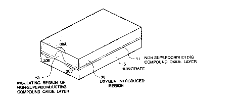
Referring to Figure 4, there is shnwn a diagrammatic perspective
view of one embodiment of tlie superconducting device in accordance
with the present invention. This embodiment is a Josephson device.
The ~osephson device includes a substrate 5 and a compound thin
film ll formed on the substrate 5. The compound thin film l1 has an
oxygen introduced region 30, which can be divided into a pair of
relatively ~ick supercollducting electrode regions 30B and 30C and an
- 25 -
extremely thin wea~ link re ion 30A between the pair of superconducting
electrode regions 30B and 30C The compound thin film 11 formed on
the substrate 5 has a planari7ed upper surface, and therefore, has a
projecting insulating region which is not introduced with oxygen and
which is positioned under the extremely thin weak link region 30A.
The compound layer 11 is formed of a compound which itself is not
a superconductor but which will become an oxide superconductor when
oxygen ions are injected. Therefore, an appropriate amount of oxygen is
introduced into the compound thin film 11~ the oxygen introduced region
30 becomes an oxide superconductor. For example, this compound
includes a compound oxide which is composed o-f the same constituent
elements as those of an oxide superconductor but includes the oxy;,en
amount less than that of the oxide superconductor.
Now, the process for manufacturing the above mentioned
superconducting device will be described with reference to Figures 5A to
SF. In the embodiment which will be Aescribed below, a Y-Ba-Cu-O type
compound oxide superconductor material is used for forming the oxide
superconductor thin film.
First, a substrate 5 having a flat upper or principal surface is
prepared as shown in Figure SA. This substrate S is formed of as a MgO
(100) substrate. As mentioned hereinbefore, however, the substrate can
be formed of another insulating substrate such as a CdNdA104 (001)
substrate or others. If these substrates are used, a c-axis orientated oxide
superconductor thin film having a large critical current density in a
direction in par~llel to the substrate surface can be formed on the
substrate.
- 26 -
~5~
As shown in Figure ~B~ a compound oxide layer ll of Y-Ba-Cu-O
compound oxide is formed on a principal surface of the substrate S by for
example an off-axis sputtering. or a reactive evaporation process. The
Y-Ba-Cu-O compound oxide of the compound oxide layer ll has an
intentionally reduced oxygen conte nt which is smaller than a
YlBa2Cu3O7 x oxide superconductor which shows superconductivity.
Therefore, the Y-~a-Cu-O compound oxide of the compound oxide layer
11 does not show superconductivity even if it is cooled.
In this example, the off-axis sputtering is performed under the
condition that a sputtering gas is composed of Ar and ~2 at the rate of Ar
: O2 = 90%: 10%, the spu~tering gas pressure is lOPa, and the
tempera~ure is 700~C.
Then, as shown in Figure SC, patterned photoresists 93A, 93B and
93C is deposited on the compound thin film 11 so as to cover a region in
which a weak link is formed in future, so that the amount of oxygen
ion-implanted into a reoion corresponding to the weak link is suppressed
in a later oxygen ion implantation process.
As shown in Fi;,ure SD, an exposed portion of the compound thin
film ll nre etched by n rc~cti~c ion ctching proccs~ or an ion mil]ing
using Ar-ions, so that shallow grooves 14A and lSA are formed on the
surface of the compound thin film l1. These grooves 14A and lSA are
formed in order to ensure that a sharply shaped extremely thin oxide
superconductor region can be formed for the weak link, as seen from a
later description. Therefore~ if a shallow stepped portion can be formed
by an etching process with a good controllability, the compound thin film
l l excluding the weak link portion can be ~miformly etched.
- 27 -
~s~
Thereafter, the patterned photoresists 93A and 93C is removed so
as tn leave only the photoresist 93B corresponding to the weak link
forrnation region, and oxygen ions are deeply ion-implanted into the
compound oxide thin film l l so that a pair of oxygen injected regions 2
and 3 are folmed in the compound thin film l l as shown in ~igure 5E.
The pair of oxygen injected regions 2 and 3 become an oxide
superconductin~ region, and has a depth near to the thickness of the
compound ~in film ~ l. On the other hand. an oxygen ion injected region
is not forrned in a central portion masked by the photoresist 93B.
After the remaining photoresist 93B is removed, the substrate S is
heated in an oxygen atmosphere, so that the oxygen injected regions 2 and
3 are enlarged? and oxygen contained in the oxygen atmosphere is
diffused from the surface of the compound thin film I l which had been
m;~kerl by the photoresist 91 in the previous process. Since oxygen in the
compound thin film 2 is easy to diffuse in a horizontal direction, oxygen
introduced from a side surface 14 and 15 of the grooves 14A and l5A in
the previous process diffuses in a horizontal direction, and ~lnally, the
oxygen injected regions ~ and 3 are coupled with the diffused region, and
this diffused region constitutes a weak link ]0. This heat-treatment is
perforrned at a temperature of 400~C.
Thus, the superconducting electrode regions 30B and 30C deeply
injected with oxygen ions, and the weak link portion 30A horizontally
di~fused with oxygen are formed. In the completed device, the
superconducting layer in the weak link portion 30A has an effective
thickness of five to ten nanometers.
In the above mentioned four embodiments, the oxide
superconductor thin film can be fomled of not only the Y-Ba-Cu-O type
- 28 -
'
compound oxide superconduc~or material. but also for example a
Bi-Sr-Ca-Cu-O type compound oxide superconductor mlaterial~ and a
Tl-Ba-Ca-Cu-O type compound oxide superconductor material.
l'he invention has thus been shown and described with reference to
the specific embodiments. However~ it should be noted that the present
invention is in no way limited to the details of the illustrated structures
but changes and modifications may be made within the scope of the
appended claims.
~9
~- . . '