Note: Descriptions are shown in the official language in which they were submitted.
AUXILIARY BATTERY OPERATION DETECTION CIRCUIT
The pr~sent invention generally relates to ~attery
powered electronic devices, ~nd more particular, to
electronic devices having primary and auxiliary battery
~upplies of differing voltages.
Battery powered personal computers are becoming
very popular, particular as the computers get smaller
and smaller. This makes them highly portable ~o that
they can be used in practically any location, often
quite far ~rom sources of electrical power. This
possible inaccessibility of power means that long term
battery operation is very important. When going to a
remote location it is common to utilize several sets of
additional batteries which have been charged prior to
leaving the source of availabl~ power. As a battery
discharges, it is replaced with a charged battery and
operations can continue. In this manner the total
operating time of the computer before a power down or
loss of power situation can greatly exceed that of a
single battery.
However, one problem that can occur in the battery
changing situation i5 that the user may not be able l:o
saYe the information present in t~e computer when the
battery needs to be replaced and before the ~attery
reaches a dead battery level. That is, the battery may
need to be replac~d but the computer may be in the
middle of an operation whioh cannot be interrupted. In
-2-
these cases any data present in the memory of the
computer would be lost when the dead battery level is
reached and any operations would have to be completely
reinitiated and any data reentered. This is obviously
S an undesirable condition. To this end the computer
~ystem may contain a smaller, low power auxiliary
battery which i~ not capable of providing energy to a
~ully operating unit, but can operate a temporary power
source if the computer is in a standby or low power
mode. ~he use of the auxiliary battery allows the
primary battery to be replaced without loss of data to
the computer system. ~he use of the auxiliary battery
thus allows for extended operation of the computer
system without loss o~ data.
Typically the auxiliary battery will have a lower
output voltage than the primary battery. The auxiliary
battery preferably is very small and so fewer
individual cells are used to ~orm the auxiliary
battery, resulting in this lower voltage. However, the
computer system contains battery voltage monitoring
circuitry to shut down the power supply, and
consequently the computer, to prevent damage to the
primary battery by deeply discharging the battery and
to the computer should a primary battery having too low
of a voltage be installed. The voltage of the
auxiliary battery is well into the region that would
normally be consid~red dead or fully discharged if the
primary battery was active. Yet the auxiliary battery
is ~ully operational and the computer system can
continue to operate in the standby mode. Thus the
battery voltage monitoring circuitry in the computer
system must be able to determine when the primary
battery i5 going dead or when it has been removed and
operation is being continued on the auxiliary battery.
3~
- :. .
:
? r~
~3~
In a computer system embodying the present
invention a DC-DC power supply utilized in the computer
system monitors the battery voltage and produces proper
operating voltages for the computer system. ~f the
voltage level from thQ batteries is in thQ discharged
or dead voltage range of the primary battery and the
computer system is in standby mode, a timer is started
timing this entry into the low voltage state. If the
battery voltage drops to the level of the auxiliary
battery before the timer's period has elapsed,
auxiliary battery operation is propar because this is
an indication that the primary battery has been
removed, the voltage change being abrupt. If the
battery voltage is to slowly sag or drop, this is an
indication that the primary battery is still present
and is further discharging. This is a case to shut
down the power supply and the computer system.
Therefore if the battery voltage is still above the
auxiliary battery level after the timer completes, the
power supply shuts down and no auxiliary battery
operation is indicated. Thus by waiting for an
interval after entry into a dead primary battery state
before shutting down, the switchover to the auxiliary
batteries can be detected and computer system operation
continued.
A better understanding of the present invention
can be obtained when the following detailed description
of the preferred embodiment is considered in
conjunction with the following drawings, in which~
Figure 1 is a block diagram of a computer system
incorporating the present invention;
Figure 2 is a schematic diagram of the DC-DC power
supply of the computer sy~tem of Figure l;
_4_
Figure 3 is a block diagram of the monitor and
control circuit of Figure 2;
Figure 4 is a schematic diagram of portions of the
circuitry of the voltage monitor circuitry of Figure 3;
5Figure 5 is a schematic diagram of portions of the
standby circuitry of Figure 3;
Flgure 6 i9 a schematic diagram of portions of the
power good circuitry of Figure 3;
Figure 7 is a schematic diagram of portions of the
power up circuitry of Figure 3; and
Figure 8 is schematic diagram of portions of the
oulse width modulation control circuitry of Figure 3.
Referring now to Figure 1, a battery powered
computer system is generally shown. An AC adaptor 20
is connected into an AC input, which is typically
available from the wall or o~her conventional source,
and provides a DC output voltage, preferably in the
range of 16.8 to 26 volts. The lines or signals
provided by the. AC adaptor 20 are referred to as V~T~
and ground, representing the positive and ground
voltage supply lines. Connec~e~ between the V~AIT line
and ground is a primary battery 22 and a DC-DC power
supply 26. An auxiliary battery 24 has its negative
terminal connected to ground and its positive terminal
connected to the cathode of a current limiting diode 23
and the anode of a diode 25. The anode of the current
limiting diode 23 and the cathode of the diode 25 are
connected to the V~ line. The current limit diode 23
prevents the auxiliary battery 24 from overcharging and
the diode 25 allows the auxiliary battery 24 to deliver
power. Additionally, the remaining portions of the
computer 28 receive the V~ and ground signals for
providinq certain levels of power. The primary battery
22 in the preferred embodiment has an operating voltage
"
~. 5 _ ~, r~
between 16.8 and 26 volts, while the auxiliary battery
24 has an operating voltage between 8 and 14 volts.
Both the primary battery 22 and the auxiliary battery
24 are comprised of a plurality of individual cells of
desired capacity and voltage, Preferably thQ primary
battery 22 is much larger than the auxiliairy battery
24, which can supply only low amounts of power for
short intervals. The DC-DC power supply 26 converts
the voltage it receives on the V~IS line to a +5 volt
line, which is the primary operating voltage for
circuitry in the computer 28, and a -28 volt line,
which i5 used by the liquid crystal display in the
preferred embodiment of the computer 28. The DC-DC
power supply 26 provides the LBATTl, LBATT2 and
POWERGOOD signals to the computer 28 to inform it of
voltage status. A STANDBY signal is provided from the
computer 28 to the DC-DC power supply 26 to indicate
standby or low power operation. Additionally, a 5VSENS
signal, the 5 volt sense signal, is returned from the
computer 28 to the DC-DC power supply 26 so that the
actual re~ulation point for the +5V line is closer to
the load as desired by the computer system designer and
is not simply the voltage present at the DC-DC power
supply 26.
Referring now to Figure 2, the DC-DC power supply
26 is generally shown. A monitor and control circuit
30 is used to control operation o~ the DC-DC power
supply 26. This monitor and control circuit 30 is
preferably a single CMOS integrated circuit for lower
power consumption, flexibility of design and space
saving. A rasistor divider ladder 32 is connected
between the V~T line and ground and provides a series
o~ different voltage levels to the monitor and control
circuit 30 to allow monitoring of various battery
levels against a single reference voltage in the
, , , :.;. ,. . ; ., . ... - ~ -... -~ . .
. . . , ., . . ;,
; i . , ., ,
~ ~ c, ~J ,' S~
-6-
monitor and control circuit 30. The emitter of a power
supply turn on PNP transistor 34 is connected to the
V~ line. A capacitor 36 is connected between the
base of the transistor 34 and the V~TT line to provide
noise and switching decoupling. A resistor 38 is
connected between the V~ line and the base of the
transistor 34, with a resistor 40 connected between the
base of the transistor 34 and one terminal of a power
switch 42. The second terminal of power switch 42 i5
connected to ground, so that when the switch 42 is
closed, the transistor 34 is activated, allowing power
to be transmitted to the remaining portions oP the
power supply circuitry. Thus in this fashion the power
switch 42 iB used to turn off and turn on the DC-DC
power supply 26 and thus the com~uter 28.
The collector of the power supply turn on
transistor 34 is connected to one terminal of a
resistor 44 whose second terminal is connected to a
PWMTRIG input of the monitor and control circuit 30. A
capacitor 46 is connected between the PWMTRI5 input and
ground to provide a delay. The PWMTRIG input is used
to indicate that power is now being provided and the
computer 28 is to be turned on. The PWMTRIG input
signal is also provided to the input of an oscillator
components block 48. The monitor and control circuitry
30 includes a pulse width modulated power supply
circuit for generating the control signals used in the
DC-DC power supply 26. To this end, various oscillator
components, such as resistors and capacitors, are
needed to help prcvide a basic clocking signal to the
PWM circuitry. The oscillator components 4~ are also -
connected to a line or signal referred to as ~DD~ the
power supply voltage for this portion of the DC-DC
power supply 26, and to ground.
: - , . : ~, . . .
-7-
An n-channel junction field effect transistor
(JFET) has its drain connected to the collector of the
power supply turn on transistor 34 and its source
provide~ the VDD signal, the controlled voltage for
this portion of the circuitry. The gate signal to the
JFET 50 is provided by an output referred to as the
VDDREG output or VDD regulator control output which is
provided by the monitor and control circuit 30.
The VDD signal is provided to the monitor and
control circuit 30 for powering its operation and is
additionally provided to the input of an adjustable low
power regulator 52, such as an LP2951 by National
Semiconductor. The output of the regulator 52 is
re~erred to as the VREF signal, which is provided to
the monitor and control circuit 30 to be used as a
reference voltage in comparing the various voltages
developed by the resistor divider ladder 32.
Additionally, the VREF signal is provided as an input
to the 28 volt sense circuitry 54, which also receives
a -28 volt signal which is produced by the DC-DC power
supply 26. Further, the 28 volt sense circuity 54 is
connected to ground and produces a signal referred to
as NEG W, or negative undervoltage, which is provided
to the monitor and control circuit 30 for indication of
a negative output undervoltags condition.
The VREF signal is provided as a comparison input
to the 5 volt sense circuitry 56, which also receives
the SVSENS signal from the computer 28. The 5 volt
sense circuitry 56 provides three signals to the
monitor and control circuit 30, these signAls being the
ERRPOS, ERRNEG and O~PG or positive ~rror, negakive
error and overvoltage signals for use by the monitor
and control circuit 30 in controlling output pulse
width and det~rmining 5 volt output overvoltage and
undervoltage conditions. The monitor and control
;, ~ ' ! , , , . . ~ . ~
... : ' ' ' , .. ' : ' ,
-8~
circuit 30 also receives a STANDBY signal from the
computer 28 to indicate that the computex system has
entered a low power mode used to conserve battery life.
The monitor and control circuitry 30 produces
three signals based on the level o~ the VBA~ line and
operation of the DC-DC power supply 26. These signals
are referred to as LBATTl, LBATT2 and POWERGOOD. The
LBATT1 and LBATT2 si~nals represent the primary battery
22 entering first and second low ~attery level states,
which are respectively low and lower voltages. The
POWERGOOD signal is an indication that the DC-DC power
supply 26 is operating properly and that proper voltage
levels are being provided to the computer 28.
The VDD signal is provided to the gate of n-
channel enhancement mode power MOSFET S0. The source
of the MOSFET 60 is connected to the MDRIVE signal
provided by the monitor and control circuit 30, which
is a control signal used to switch one portion of the
switching power supply used in the DC-DC power supply
26. one terminal of a resistor 62 is connected to the
drain of the MOSFET 60~ The second terminal of the
resistor 62 is connected to the cathode of a diode 64,
whose anode is connected to the VDD line. Also
connected to the cathode of the diode 64 is one
terminal of a capacitor 66 and the power supply input
for a buffer driver 68~ The signal input of the buffer
driver 68 is connected to one terminal of a resistor
70, whose other terminal is connected to thQ drain of
the MOSFET 60. The ground reference of the buffer
driver 68 is connected to it the second terminal o~ the
capacitor 66, one terminal of a capacitor 72 and the
anode of a diode 74. The cathode of the diode 74 and
the second terminal of the capacitor 72 are connected
to the input o~ the buffer driver 68. The local ground
reference for the buffer amplifier 68 is connected to a
_ 9 ~ , ,' "
first terminal of a primary winding of a transformer
80. A resistor 82 is connected between this
transformer winding terminal and the output of the
buffer driver 68. The output of the buffer driver 68
is further connected to the gate of a n-channel
enhancement power MOSFET 84. The drain of the MOSFET
84 i connected to the V~ line, with a filter
capacitor 86 connected between the V~T signal and
ground to provide local filtering for the DC-DC power
supply 26. The source of the MOSFET 84 is connected to
the first terminal on the primary of the transformer 80
to provide the switching component to allow energy to
flow from the batteries into this leg of the
transformer 80. The cathode of a diode 92 is connected
to the gate of ~he MOSFET 84, with the anode connected
to an MGATE signal provided to the monitor and control
circuit 30. The MGATE signal is used to provide
feedback on the output pulse control state~
The final component connected to this first
terminal of the primary winding of the transformer 80
is the drain of an n-channel enhancement power MOSFET
90. The gate of the MOSFET 90 receives the RDRIVE
si~nal produced by the monitor and control circuit 30,
which is effectively the inverse of the MDRIVE signal
when the power supply.is operating. The source of the
MOSFET 90 is connected to ground.
The second terminal of the primary winding of the
trans~ormer 80 is considered to be the ~5 volt line and
is connected to a capacitor 92 which has its other
terminal connected to ground. The cathode of a Zener
diode 94 is connected to the +5 volt line, while the
anode of the Zener diode 94 is connected to one
terminal of a reeistor 96, one terminal of a capacitor
98 and the gate of a silicon controlled rectifier (SCR)
100. The second terminals of the resistor 96 and
, - ~ ., , . -, :
.; : . . ~ . . . , . .
~10 `
capacitor 98 are connected to ground. The anode of the
SCR 100 is connected to the ~5 volt line, while the
cathoda of the SCR 100 is connected to ground. The
Zener diode/SCR circuitry provides an overvoltage
clamping circuit on the ~5V output ~or protection.
The secondary w1ndiny of the transformer 80
produces the -28 volt signal. One terminal of the
secondary winding is connected to ground, along with a
capacitor 102 and the cathode of a diode 104. The
second terminal of the capacitor 102 and the anode of
the diode 104 are connected to the -28 volt line, with
the anode of a diod~ 106 also being connected to this
line. The cathode of the diode 106 is connected to the
second terminal of the secondary winding of the
transformer 80. Thus this second winding provides a
simple rectified -28 volt output for use by the
computer 28.
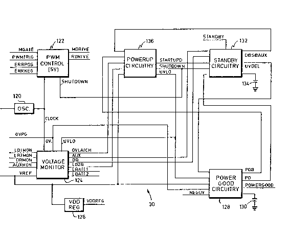
Referring now to Figure 3, the monitor and control
circuit 30 is shown in more detail. The signals from
the oscillator components 48 are connected to an
oscillator 120. The oscillator 120 produces a clock
signal referred to as CLOCK. This CLOCX signal is
provided to a PWM control module 122. The pulse width
modulation (PWM) control module 122 receives the MGATE
signal, the PWMTRIG signal, the ER~POS signal and the
ERRNEG signal to control its operations and provides
the MDRIVE and RDRIVE signals to the transistors 60 and
90. Additionally, the PWN control module 122 receives
a signal referred to as SHUTDOWN which disables
operation of the PMW control module 122 when in a high
state.
The CLOCX signal is also provided as one input to
a voltage monitor circuit 124. Other inputs to the
voltagQ monitor circuit include the LBlMON, LB2MON,
DBMON and AUXMON signals, which are provided as the
,, ~ ., ~ , ~ , ., :. , .
:- . ~ , : . . - ............................... .. .; .
-
~ 5 iJ . ? ~J '
outputs of the resistor divider ladder 32. Thase
signals refer, respectively, to the first low battery
voltage level, the second lower battery voltage level,
the dead or discharged battery voltage level and the
auxiliary battery voltage level as appropriately
divided ~or comparison with the VREF signal, which is
an additional input to the voltage monitor 124. The
OVPG signal doveloped by the 5 volt sense circuitry 56
is an input to the voltage monikor 124 so that certain
signals can be disabled or latched as appropriate. The
W LO signal is a further input relating to undervoltage
conditions and is high when not undervoltage. Outputs
of the voltag~ monitor 124 include the LBATTl and
LBATT2 signals, which are provided to the computer
system 28; a signal referred to ~s LB2B, which is an
inverted version of tAe LBATT2 signal; the DB signal,
which when high indicates a dead battery level; the AUX
signal, which when high indicates that a voltage above
that of a fully charged auxiliary battery level is
present; and the OVLATCH signal or overvoltage latched
signal.
The VREF signal is additionally provided to the
VDD voltage regulatox 126 which produces the VDDREG
signal to activate the JFET 50 to allow control of the
25 VDD signal level.
The VREF signal is additionally an input to the
power good circuitry 128. Other inputs to the power
good circuitry 128 are the NEG W signal, the OVPG
signal, the W LO signal and a signal referred to as
WDEL, which indicates when high that an undervoltage
delay period has completed. The outputs of the power
~ood circuitry 128 are the POWERGOOD signal, which is
provided to th~ computer 28 to indicate that a stable
and satisfactory 5 volt signal is present; the PO
signal, which an internal version of the POWERGOOD
.: ~ ~ , ......... . .
--12 ~
signal; and the POB signal, which is a latched version
of the PO signal and indicates when high that valid
power is pr~sent. ~ capacitor 130 is connected between
the power gaod circuitry 128 and ground for use in
developing a timing delay for developing the POWERGOOD
signal.
The PO .signal is provided as one input to the
standby circuitry 132. Other inputs to the standby
circuitry 132 are the STANDBY signal as received from
the computer 28, the AUX signal, the DB signal, a
signal referred to as STARTUPB, which indicates that a
start up sequence is in operation and the SHUTDOWN
signal. The outputs of the standby circuitry 132 are
the DBSBAUX signal, which indicates a dead battery,
standby and auxiliary situation; and the W DEL signal,
which when high indicates that the undervoltage delay
has been completed. Additionally, a capacitor 134 is
connected between ground and the standby circuitry 132
to provide a delay period used in developing the W DEL
signal and timing to control the auxiliary switchoYer
signals.
The STARTUPB, SHUTDOWN and UVLO signals are
developed by power up circuitry 136. The inputs to the
power up circuitry 136 are the POB signal, the OVLATCH
signal, the LB2B signal, the YREF signal and the
DBSBAUX signal.
These various modules are explained in more detail
in the following figures and description. Referring to
Figure 4, the voltage monitor circuitry 124 is s~own in
more detail. The VREF signal is connected to the
inverting input of 4 comparators 150, 152, 154 and 156.
These comparators 150, 152, 154 and 156 are used to
compare a~ainst the monitoring voltages received from
the resistor divider ladder 32. The LBlMON signal is
connected to the noninverting input of the comparator
- - ;.. ;
, : . .
- :,: . . . . .
- , ~ . , . :
~; . .
, , ~
~ ~ ci ~J
--13 ~
156, while the LB2MON signal is conneoted to the
noninverting input of the comparator 154. The DBMON
signal is provided to the noninverting input of the
comparator 152, while the AUXMiON signal is provided to
the noninverting input of t~ie finàl comparator 150.
The LBlMON signal voltage division from the V~TT line
i5 set such that when the primary baitteries are
dischar~ed to a ~irst level, the output o~ the
comparator 156 goes low. Similarly, the LB2MON signal
level is divided from the VBATT line such that when the
batteries have discharged to a second level, which is
lower than the LBlMON level, the output of the
comparator 154 goes to a low level. Similarly, when
the D~MON signal is below a given level which is
indicative of a dead primary battery 22, for example
16.8 volts in the preferred embodiment, the output of
the comparator 152 goes to a low level. Finally, when
the VBATI signal goes below a lower value which is
indicative of the auxiliary battery 24 operation, the
AUXMON signal has a value less then the VREF signal and
the output of the comparator 150 goes low.
The outputs o~ the comparators 150, 152, 154 and
156 are connected to the D inputs of two 2 bit D-type
flip-~lops 158 and 160. The CLOCK signal from the
oscillator 120 is proYided as the clocking input to
both flip-flops 158 and 160. The W LO signal is
connected to the inverted resPt input of the flip-flop
160, while the UVLO signal is connected to the inverted
set input of a flip-flop 158. In the particular
preferred embodiment, the noninverted outputs of the
flip-flops 158 and 160 are utilized. Thus the
noninverted output of the flip-~lop 158 corresponding
to the D input receiving the output of the comparator
150 is the AUX signal, so that the AUX signal is high
when the V~ line level is above that at which the
-14~ ;3
auxiliary battery 24 is expected to be operating. The
noninverted output of the flip-flop 158 corresponding
to the D input receiving the output of comparator 152
is connected to an inverter 162, whose input i5 the DB
or dead battery signal. Therefore when the primary
battery 22 is above the level which is considered to be
fully discharged or dead, ~he DB signal is low, and is
high when the battery 22 is considered discharged. The
noninverted output of flip-flop 160 corresponding to
the D input connected to the comparator 154 is
considered to be the L~2B signal and is connected to
the i~put of an inverter 164. The output of the
inverter 164 is the LBATT2 signal, so that when it is
high, the primary battery 22 condition is at or below
the second low voltage level. The noninverting output
of the flip-flop 160 corresponding to the D input
receiving the output of the comparator 156 is provided
to the input of an inverter 166 whose output is the
LBATT1 signal. Thus when the LBATTl signal is high the
primary battery 24 is below the first low voltage
level. Therefore the divided battery voltage is
received at the inputs of the comparators 150-156,
compared with the VREF signal, periodically latched
into a series of flip-flops 158 and 160 to allow
relatively stable siynals to be developed, and inverted
if appropriate.
The OVPG signal is connected to one terminal of a
resistor 168. The second terminal of the resistor 168
is connected to the noninverting input of a comparator
170. ~ resistor 172 is connected between the
noninverting input of the comparator 170 and ground,
thus forming a resistor divider with resistor 168. The
VREF signal is provided to the inverting input of the
comparator 170 so that when the level of the OVPG
signal as provided ~y the 5 volt sense circuitry 56
:, ., , : ,
: ~
", : ,, : .
~iJ 1 ~ ~
--15--
indicates that the 5 volt level is too high, the output
of the comparator 170 is at a high level. The output
of the comparator 170 is connected to the input of an
inverter 172. The output of the inverter 172 is
conneoted to one input of a 2 input NAN~ gate 174. The
output of the NAND gate 174 is provided to one input of
a 2 input NAND gate 176. The output of the NAND gate
176 is connected to the seco~d input of the NAND gate
174 and is referred to as the OVLATCH signal so that
when an overvoltage condition does occur it is latched
in by the latch formed by the NAND gates 174 and 176
and the OVLATCH signal stays set until an undervoltage
condition occurs. The W LO signal is provided as the
sacond input to the NAND gate 176 so that the OVLATCH
signal is high when an undervoltage condition occurs
and until the next overvoltage condition occurs.
Referring now to Figure 5, the standby circuitry
132 is shown in more detail. The SHUTDOWN signal
indicating that the 5 volt power supply should be shut
down is provided as the input to a inverter 200. The
output o~ the inverter 200 is connected to the gate of
an n-channel enhancement MOSFET 202 and to the gate of
a p-channel enhancement MOSFET 204. The drain of the
MOSFET 204 is connected to a constant current source
206 whish is connected to th~ VDD line. The source of
the MOSFET 204 is connected to the drain of the MOSFET
202, to the drain of an n-channel enhancement MOSFET
208 and to the gates of the MOSFET 208 and an n-channel
enhancement MOSFET 210. The sources of the MOSFET's
202, 208 and 210 are connected to ground. The drain o~
the MOSFET 210 is connected to the inverting input of a
comparator 212 and to the output of a current soure
214. The current source is connected to the VDD line
for power~ Thus in this manner if the SHUTDOWN signal
is not rec~ived, the MOSFET 204 i5 turned off and the
., ,, - . .,. , -
.. ..
.: ' ;' , ' ' ', ~ . ! ' : .
? i,~
--16--
MOSFET 202 is turned on, so that the MOSFET 210 is
turned of f and the inverting input of the comparator
212 is not clamped to ground.
The noninverting input of ~he comparator 212 is
5 connected to a rei~erence voltage referred to as Vcc~p
which is used in the standby circuitry 13a. The output
of the comparator 212 is connected to an inverter 214
whose output is the WDEL signal. The inverting input
of the comparator 212 is also connected to one through
10 terminal of a transfer gate 218. The second through
terminal of the transfer gate 21û is connected to a
capacitor 134 which is connected to ground. Thus when
the transfer gate 218 is activated, the voltage at the
invertin~ input of the comparator 212 i5 the capacitor
15 134 voltage if the SHUrDOWN signal is not activated or
ground if the system is in shut down.
The inverted control input of the transfer gate
218 receives the PG signal or internal power good
signal, which is also inverted by an inverter 222 whose
20 output is connected to the noninverted control input of
the transfer gate 218. Thus in this manner when the
power is good the transfer gate 218 is off, while when
the power is bad the transfer gate 218 is activated.
Therefore before tha PG signal is high, that is, during
25 power up, the capacitor 134 serves to set the
undervoltage detection delay time.
The output of the inverter 222 is additionally
connected to the inverted control input of 3 transfer
gate 224, wh~se noninverted control input receives the
30 PG signal. One through terminal of the transfer gate
224 is connected to the capacitor 134, while the other
through terminal is connected to the output of a
constant current source 226, which is connected to the
VDD line to receive power. The constant current source
35 226 is also connected to the inverting input of a
17 ~ r
comparator 228 and to the drain of a n-channel
enhancement MOSFET 230. The Vc~ signal is provided to
the noninverting input of the comparator 228. The
source of the NOSFET 230 is connected to ground, while
the gate is connected to the output of a two input NAND
gate 232. The two input signals to the NAND gate 232
are the AUX and DB signals. Thus when the battery
voltage is above the auxiliary battery voltage sense
level and below the dead battery sense level,
indlcating the possible entry into auxiliary mode
operation, the MOSFET 230 is turned off and the
invertiny input of the comparator 228 is not grounded.
The transfer gate 224 is activated as the output
voltage levels are adequate, so the capacitor 134
begins charging. However, when the voltage is above
the dead battery lev~l or at the auxiliary battery
level, then the inverting input to the comparator 228
is grounded by the MOSFET 230. In this condition if
the power is satisfactory as indicated by the PG
signal, the capacitor 134 is also grounded. Thus
during power good conditions the capacitor 134 is used
to set the primary to auxiliary battery switchover
delay time.
The output of the comparator 228 is provided to
the input of an inverter 234. The output of the
inverter 234 is provided to the input of a second
inverter 2~6 and to the clocking input of a D-type
flip-flop 238. The output of the inverter 236 i~
provided to the inverted clocking input of the flip-
flop 238. The STARTUPB signal i5 provided to theinverted set input, while the D input is con~ected to
ground. The ST~RTUPB signal connection is used to set
the ~lip-flop 238 on start up so that the dead battery
ti~ing capacilities are available. The noninYerted
output of the flip-flop 238 is the DBSBAUX signal
, . ........... . .......... .. , . , ....... . .... ... : ..
.: . ,, ~. , .. : , :: :,: .,.: : :- ,; - . ,::
, ! ' .: ' ' ~ !' . ' . ` `
, '. ' :: :',:. '' ;:'';: '' . '' ':' . " " . "'
1~ ~v ' . . J ~ Ci ','i
-18-
which, when high, generally indicates that the dead
battery, standby and auxiliary mode is active.
The inverted reset input o~ the ~lip-flop 238 is
provided hy the output of a two input N~ND gate 240.
The DR signal i5 one input to the NAND gate 240, while
the second lnput is the output of a two input NAND gate
242. One input to the NAND gate 242 is the PG signal,
while second input is the output of an inverter 244.
The input to the inverter 244 is provided by the output
of a NOR gate 246 which has all of its inputs connected
to the sources of two p-channel enhancement MOSFET
transistors 248 and 250 and an n-channel enhancement
MOSFET 252. The drains of the MOSFET's 248 and 250 are
connected to the VDD line. The PG signal is provided
to the gate terminal of the MOSFET 248, while the DB
signal is provided to the gate of the MOSFET 250. The
PG signal is also provided to the gate o the ~OSFET
252. The drain of the MOSFET 252 is connected to the
source of an n-channel enhancement MOSFET 254 whose
drain is connected to the STANDBY signal. The gate of
the MOSFET 254 i9 connected to the DB signal. Thus the
input to the NOR gate 246 i5 high if the power is not
good or a dead battery condition i5 not present and if
the system is in standby, the power is good and a dead
battery condition is present. Therefore the flip-flop
238 is released from a reset condition when the primary
battery 22 is not dead cr the power is good and the
system is in standby and the battery level is not at or
below the dead threshold. If the battery 22 is dead;
the power is not good; or the battery 22 is dead, the
power is good and standby mode is not activated, the
DBSBAUX signal is held low causing a shutdown
condition. If the system has been in normal usage
where the battery 22 has reached the dead battery
voltage level, the power is good and standby mode is
acti~ated, when the auxiliary mode is antered before
the capacitor 134 charges to a sufficient level, the
DBSBAUX signal stays high. But i~ the auxiliary mode
is not entered in a sufficient time the D~SBAUX signal
is set low by clocking the flip-flop 238~ The DBSBAUX
signal can only be set to a high level by the STARTUP~
signal being low, which only occurs during the start up
phase after the power switch 42 has been closed. Thus
to restart the DC-DC power supply 26 after a dead
battery shutdown, the power switch 42 must be opened
and closed.
The power good circuitry 128 is shown in more
detail in Figure 6. The 28VSENS signal is provided to
the inverting input of a comparator 260. The
noninverting input of the comparator is connected to
one terminal of a resistor 262 whose other terminal is
connected to ground. The noninverting input of the
comparator 260 is further connected to one terminal of
a r~sistor 264, whose second terminal is connected to a
resistor 266 and to the inverting input of a second
comparator 268. The second terminal of the resistor
266 recei~es the VREF signal. The OVPG signal,
essentially the +SVSENS signal, is provided to the
noninverting input of the comparator 268. The outputs
of the comparators 260 and 268 are connected together
and to the gates of an n-channel enhancement MOSFET 270
and a p-channel enhancement MOSFET 272. The drain of
the MOSFET 272 is connected to the output of a constant
current source 274 which is also connected to the VDD
line for power~ ~he source of the MOSFET 272 is
connected to the drain of the MOSFET 270, the gate and
drain of an n-channel enhancement MOSFET 276 and to the
gate of an n-channel enhancement MOSFET 278. The
sources of the MOSFETs 270, 276 and 278 ire connected
to ground. The drain of the MOSFET 278 is connected to
': '; ' ' - : . , ' ,, ', ,'', ,~. " '' : .
~ r~ r~ r~
--20--
the output of a constant current source 280, which
receives its power from the VDD signal; to the
noninverting input of a compaxator 282 and to one
terminal of a capacitor 130, whose other terminal is
connected to ground. ~he inverting input of the
comparator 282 is connected to the VREF signal. The
capacitor 130 is the power good delay capacitor. Thus
if the 5 volt output is too low or the magnitude of the
-28 volt level is too low (that is, not sufficiently
negative), the MOSFET 278 is turned on and the
capacitor 130 is clamped to ground.
The output of the comparator 28z is connected to
the drain of an n-channel enhancement MOSFET 284 whose
source is connected to ground and whose gate i
connected to the output of an inverter 286. The input
of the inverter 286 receives the W LO signal. In this
manner if the UVLO signal is low, indicating a VDD
undervoltage condition, the output of the comparator
282 is clamped to ground. After the undervoltage
condition is cleared the comparator 282 output is
released so that the voltage on the capacitor 130
determines the output of the comparator 282. The
output of the comparator 282 is also provided to the
inputs of two inverters 288 and 290. The output of the
inverter 288 is provided to the input of an inverter
292 whose output is the PG signal. The output of the
inverter 290 is provided to the input of a inverting
buffer driver 294 whose output is the POWERGOOD signal.
Additionally, the output of the comparator 282 is
provided to the input of a Schmidt trigger inverter 296
whose output is provided as one input o~ a 2 input NAND
gate 298, to the clocking input of a D type flip-~lop
300 and to the input of an invert~r 302. The output of
the inverter 302 is provided to the inverted clock
input of the flip flop 300. The D input of the flip-
.
-21- f:.J<~ J ~t '~
flop 300 receives the VDD or a positive signal level.
The inverted reset input Of the f1iP-f1OP 300 iS
connacted to the W LO signal. The inverted output of
the flip-flop 300 is connected to one input of a 2
input NAND gate 304.
The W LO signal is connected to the second input
of the NAND qate 298, whose output i5 connected to the
input o~ an inverter 306. The output of the inverter
306 is connected to the inverted reset input of a D
type flip-flop 308. The UVDEL signal is provided to
the clocking input of the ~lip-flop 308 and to the
input of an inverter 310. The output of the inverter
310 is connected to the inverted clock input of the D
type flip-flop 308. The D input is connected to a high
voltage level. The inverted output of the flip-flop
308 is connected to the second input the,NAND gate 304.
The output of the NAND gate 304 is connected to the
input of an inverter 312, whose output is the PO~
signal. Thus in this manner if the output voltage goes
low at any time or if the voltage stays low past the
undervoltage delay time, the POB signal is low and
indicates that the power output is not acceptable and
the DC DC power supply 26 should be shutdown.
~eferring now to Figure 7, the power up circuitry
136 is shown in more detail. The VREF signal is
provided to the inverting input of a comparator 320.
The VDD signal is connected to one terminal of a
resistor 322 whose second terminal is connected to the
noninverting input of the comparator 320 and to one
terminal of a resistor 324. The ~econd te~minal of
resistor 324 is connected to the drain of an n channel
enhancement MOSFET 326 and to one terminal of a
resistor 328. The second terminal of resis~or 328 is
connected to ground. The source o~ the MOSFET 326 is
connected to ground, while the gate is connected ko the
.. .. . . .
. . ~ . . , .- . : :
-22
output of an inverter 330. The input of the inverter
330 is connect~d to the output of an inverter 332,
whose output is the UVLO signal. The input of the
inverter 33 a is connected to the output of an inverter
334, whose input i9 connected to th~ output of the
comparator 320. Thus the W LO signal is low until the
VDD level has reached a satisfactory point as
determined by the divider developed by the resistors
322 and 324, at which time the third resistor 328 is
switched in to perform a feedback function.
The W LO signal is additionally provided as one
input to a 2 input NAND gate 336. The second input to
the NAND gate 336 is provided by the output of a two
input NAND gate 338. One input to the NAND gate 338 is
provided by the output of an inverter 340 whose input
receives the LB2B signal. The second input to the NAND
gate 338 is provided by the output of the NAND gate
336. The output of the NAND gate 336 is provided to an
inverter 342 whose output is the STARTUPB signal, which
indicates that the battery voltage is acceptable to
start operations and the local control voltage is
satisfactory. The STARTUPB signal is provided as one
input to a four input NAND gate 344 who~e output is the
SHUTDOWN signal. The o her three inputs to the NAND
gate 344 are the POB, OVLA~CH and DBSBAUX signals.
Thus the SHUTDOWN signal is low when the dead battery,
auxiliary and standby condition is true, when a
success~ul start has occurred, whe~ the power is good
and has not been over volta~e.
Referring now to Figure 8, the PWM control module
122 is shown in more detail. The SHUTDOWN signal is
provided to the gates of three n-channel enhancement
MOSFET's ~50, 352 and 354. The sources of the MOSFETS
352 and 354 are connected to ground, while the source
of the MOSFET 350 is connected to the ERROUT signal,
-, . . . .. . . .
~ 'J ~ . J ~
-23-
which is provided as the o-ltput of an operational
ampli~ier 356. The ERRPOS signal is provided to the
noninverting input of the amplifier 356 and to the
drain of the MOSFET 352. The inverting input of the
S amplifier 356 receives the ERRNEG signal and the source
of the MOSFET 350. Thus if t~e SHUTDOWN signal is high
the two inputs to the amplifier 35fi are clamped. A
capacitor 358 is provided to a compensation input of
the amplifier 356 from its output. The SHUTDOWN signal
is also provided as a co~trnl input to the amplifier
356 to allow its interna~ operations to be shutdown.
The output of the amplifier 356 is provided to the
noninverting input of a comparator 360, with the
inverting input receiving the P~TRIG signal. The
output of the comparator 360 is connected to the drain
of the MOSFET 354 and to one input o~ a two input NAND
gate 362. Thus the output of the comparator 360 is
clamped to ground during shutdown. The second input to
the NAND gate 362 receives the CLOCX signal. The
output of the NAND gate 362 is provided to a Schmidt
trigger inverter 364 whose output is connected to an
inverter 366~ Th~ output of the inverter 366 is
connected to one input of a two input NOR gate 368 and
to one input o~ a two input NAND gate 370. The output
of the NOR gate 368 is the MDRIVE signal, with the
second input being connected to the output of an
inverter 372. The input to the inverter 372 is
connected to the output o~ a three input NOR gate 374
configured as an inverter. The inputs to the NOR gate
374 are provided by the output of an inverter 376 whose
output is referred to as the RDRIV~ signal. The input
to the inverter 376 is provided by the output o~ the
NAND gate 370. The second input to th~ NAND gate 370
is provided by the output o~ a thr~ input NOR gate
378. The SHUTDOWN signal is provided as one input to
' ~ ., ' ' ~ . .
' ^ ~ ' , , ' ' ' " ' ' ' , ' ' '~ . ' ', ' ' '
, ' ' ~ . ', , '' ' ' '. ' :
. , . . ' ' .: .
~ r~ n. --
-24-
the NOR gate 373, while the MGATE signal is provided to
the other two inputs. Additionally the SHUTDOWN signal
is provided to the input of an inverter 380, whose
output is connected to one terminal of a resistor 382,
whose second terminal is connected to the MGATE signal
and thus to the two input~ of the NOR gate 378. Thus
when the SHUTDOWN signal i5 received, the MDRIVE and
RD~IVE signals are clamped in a low state, thus
disabliny the switching power supply transistors 84 and
90, so that +5 volts is no longer developed by th~ DC~
DC power supply 26 and it is thus shut down.
Thus to recap operation, if the computer 28 is in
standby mode and the primary battery 22 is removed, the
D~ signal is developed, and assuming the power is good,
a window for the timing delay commences. How~ver, the
capacitor 134 will not charge because the AUX signal
will be low, the VBATT line heing at the auxiliary
battery 24 level. Therefore the flip-flop 238 will not
get clocked and the DBSBAUX signal will stay high.
However, if the primary battery 22 is simply
discharging and its output voltage has dropped below
the dead battery level, the timing will commence upon
crossing the threshold and the AUX signal will remain
high, thus allowing the capacitor 134 to charge,
eventually clocking the flip-flop 238 and setting the
DBSBAUX signal low, which in turns causes the SHUTDOWN
signal to go high, shutting of~ the PWM control module
122.
The foregoing disclosure and description of the
invention are illustrative and explanatory thereof, and
various changes in the size, shape, materials,
components, circuit elements, wiring connections and
contacts, as well as in the details of the illustrated
circuitry and construction may be made without
departing from the spirit of the invention.