Note: Descriptions are shown in the official language in which they were submitted.
` 2053448
Multilayer Printed Wiring Board and Process for
Manufacturing the Same
Background of the Invention
Field of the Invention
This invention relates to a multilayer printed wiring
board and manufacturing process therefor, and particularly
to a multilayer printed wiring board with a plurality of
metal wiring layers and insulation layers laminated on the
board and manufacturing process therefor.
Description of the Prior Art
In conventional multilayer printed wiring board,
multiple thin film layers are structured by alternatively
laminating insulation layers (made of polyimide resin, for
example) and metal wiring layers on a ceramic base
substrate as the foundation.
Further, in the manufacturing process for such a
multilayer printed wiring board, lamination of insulation
and metal wiring layers is started from the lowest layer
and a series of steps is repeated until the required
number of layers are completed.
Such conventional manufacturing methods where a
multilayer printed wiring board is fabricated by
repetition of conductor and insulation layers laminating
on the board include the method disclosed in
"Copper/polyimide Materials System for High Performance
Packaging" by R.J. Jenson and J. P. Cummings and H. Vora
"`- 2053448
(1984, IEEE) and the one disclosed in U.S. Pat.
No.4,434,544.
In case of such conventional multilayer printed
wiring board, since ceramic base substrate and polyimide
used for insulation layer have different thermal expansion
coefficients, thermal stress is generated at the base
substrate during forming of multiple thin film layers for
wiring, which results in residual stress between
insulation layer and base substrate. This residual stress
may lead to troubles such as cracks on polyimide resin,
separation from ceramic multilayer printed wiring board
and fracture at ceramic multilayer printed wiring board.
In addition, with recent progress toward higher density
mounting, film thickness of the multiple thin film layers
for wiring consisting of polyimide resin insulation layer
and metal wiring layer tends to be thicker. The thicker
the film thickness becomes, the larger the above residual
stress grows and the above troubles such as cracks on
polyimide resin and separation and fracture at ceramic
multilayer printed wiring board are becoming more serious.
Besides, in the conventional process to manufacture
multilayer printed wiring board, manufacturing starts at
the lowest layer first and a series of steps is repeated
for lamination of insulation and metal wiring layers until
the required number of layers are completed. This method
takes quite a long time when a large number of thin film
layers for wiring have to be formed on the ceramic base
`~ 2053448
substrate. In addition, the=e is a possibility of worse
yield, because unexpected defects may occur during too long
manufacturing time.
Summary of the Invention
An object of this invention is to provide a
multilayer printed wiring board and a manufacturing method
therefor which can reduce problems such as cracks of polyimide
resin and separation and fracture at ceramic multilayer
printed wiring board, and realize a shorter a manufacturing
time.
According to a first broad aspect, the invention
provides a manufacturing method for a multilayer printed
wiring board comprising the steps of: forming a first
multilayer interconnection by selectively laminating a first
metal wiring layer, a first insulation layer, a second metal
wiring layer electrically connected with said first metal
wiring layer, and a second insulation layer, on both sides of
a ceramic substrate having through holes at predetermined
positions so as to provide a multilayer interconnection
electrically connecting the layers via said through holes;
forming a second multilayer interconnection by selectively
laminating a third metal wiring layer, a third insulation
layer, a fourth metal wiring layer electrically connected with
said third metal wiring layer, and a fourth insulation layer,
on one side of a base substrate; and placing together and
integrating said first multilayer interconnection formed on
said ceramic substrate and said second multilayer
-- 3
j~
l ~ 66446-515
2053448
interconnection formed on said base substrate under
application of pressure and heat.
According to a second broad aspect, the invention
provides a manufacturing method for a multilayer printed
wiring board comprising of: a process where a metal wiring
layer and insulation layer are laminated on both sides of a
ceramic substrate having through holes at predetermined
positions so as to provide a multilayer interconnection
electrically connecting the layers via said through holes; a
process where a multilayer interconnection is formed by
lamination of a metal wiring layer and an insulation layer on
a base substrate; a process where said ceramic substrate and
said base substrate with interconnections formed on them are
placed together and integrated under application of pressure
and heat; and a process where other ceramic substrate with
multilayer interconnections formed on them are successively
placed on said integrated ceramic substrate and all of them
are integrated under pressurized and heated conditions.
According to a third broad aspect, the present
invention provides a manufacturing method for a multilayer
printed wiring board according to the following requirements;
a process to provide multilayer interconnections on both sides
of a ceramic substrate having through holes at predetermined
positions comprises of the steps below: (a) forming ground and
connection layers on the upper and lower sides of said ceramic
substrate mutually connected via through holes; (b) forming an
insulation layer on the ground and connection layer; ~c)
forming a signal wiring layer on said insulation layer for
-- 4
. 66446-515
2053448
connection with said ground and connection layer; (d) forming
a connection bump on said signal wiring layer; (e) forming
polyimide precursor to the connection bump; and a process to
provide a multilayer interconnection on a base substrate by
alternatively laminating a wiring layer and an insulation
layer comprised of the steps below: (a) forming a ground and
connection layer on said base substrate; (b) forming an
insulation layer on the ground and connection layer; (c)
forming a signal wiring layer on said insulation layer for
connection with said ground and connection layer; (d) forming
a connection bump on said signal wiring layer; (e) applying
polyimide precursor on connection bump; and a ceramic
substrate with a multilayer interconnection formed on it is
placed on said base substrate and integrated with it under
heated and pressurized conditions.
According to a fourth broad aspect, the invention
provides a multilayer printed wiring board comprising; (A) a
first block, comprising, in order, (a) a base substrate, (b) a
first polyamide insulating layer, (c) a first signal wiring
layer, and (d) a first bump electrically connected to said
signal wiring layer; and (B) a plurality of second blocks,
each comprising: (e) a ceramic substrate, (f) second polyamide
insulating layers, respectively provided on opposite sides of
said ceramic substrate, (g) second signal wiring layers,
respectively provided on a side of said second polyamide
insulating layers, (h) second bumps electrically connected to
said second signal wiring layers, (i) a through hole provided
in said ceramic substrate, connecting said second signal
-- 5
Gt 66446 515
~i`A
2053448
wiring layers; wherein said second blocks are laminated,
wherein said second bump of said second block is connected to
the adjacent second bump of another second block; and wherein
the second bump of one second block is connected to the first
bump of the first block.
A multilayer printed wiring board of this invention
- 5a -
66446-515
' .A.
2053448
to accomplish the object above is provided with a base
substrate, a plurality of multilayer interconnections
formed by lamination of wiring and insulation layers on
said base substrate, and a ceramic substrate provided with
through holes for electrical connection of multilayer
interconnections and inserted between a pair of multilayer
interconnections.
Other and further objects and effects of the
invention will appear more fully from the following
description.
Brief Description of the Drawings
Fig. 1 is a cross sectional view to illustrate a
multilayer printed wiring board according to an embodiment
of this invention;
Figs. 2A through 2E show a manufacturing process to
form a multilayer interconnection on both sides of a
ceramic substrate according to an embodiment;
Figs. 3A through 3E illustrate a manufacturing
process to form a multilayer interconnection on a ceramic
base substrate according to an embodiment;
Figs. 4A through 4E illustrate a manufacturing
process to form a multilayer interconnection on a ceramic
base substrate according to an embodiment;
Fig. 5 shows a manufacturing process where the
ceramic substrate block shown in Fig. 2 and the ceramic
2053448
base substrate block in Fig. 4 are laminated, and
Fig. 6 shows the final process for a multilayer
printed wiring board according to an embodiment.
Description of the Preferred Embodiment
A preferred embodiment of this invention is now
described referring to Fig. 1.
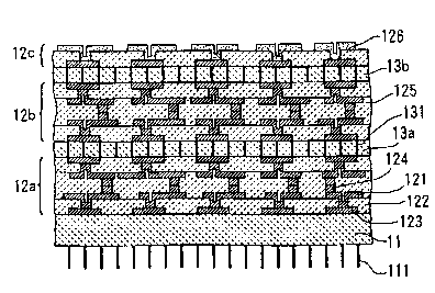
In Fig. 1, a multilayer printed wiring board of this
embodiment consists of a ceramic base substrate 11 as the
foundation, multilayer interconnections 12A to 12C thereon
and ceramic substrates 13a and 13b laminated between above
multilayer interconnections 12a and 12b and 12b and 12c.
The ceramic base substrate 11 is a simultaneously
baked alumina ceramic substrate having an internal wiring
layer made of metal such as molybdenum, provided with an
I/O pin 111 for signals and power on the rear side. This
embodiment uses a ceramic base substrate 11 having the
size of 100 mm x 100 mm and the thickness of 3 mm.
Multilayer interconnections 12a and 12b are
structured by lamination of signal wiring layers 121,
polyimide insulation layers 122, ground and connection
layers 123, connection bumps 124 and additionally
polymerized polyimide 125. The signal wiring layer 121
consists of gold plated wiring having the width of 25 ~m
and thickness of 7 ~m. X-direction and Y-direction wiring
forms a pair of signal wiring layers. Lamination of
`~ 2053448
ground and connection layers 123 on the upper and lower sides
of the signal wiring layer serves for impedance adjustment and
crosstalk noise reduction.
The polyimide insulation layer 122 is made of a
polyimide resin. Polyimide resins which can be used here
include a product from Hitachi Chemical Co., Ltd. known as
* *
" PIQ", Du Pont's product known as n PYRALYN", Toray
Industries, Inc.'s product known as n Semicofine" for
nonphotosensitive resins; and Hitachi Chemical's product known
as n PL-1200", Du Pont's product known as " PI-2702D", Toray's
product known as n Photonese", and Asahi Chemical Industry's
product known as " PIMEL" for photosensitive polyimide resins.
This polyimide insulation layer 122 causes the film thickness
between the signal wiring layer 121 and ground and connection
layer 123 to be 20 ~m. The insulation layer uses a polyimide
resin in this embodiment, but it may be made of any other
organic resin.
Signal wiring layers 121 are electrically connected
by the connection bump 124 in the additionally polymerized
polyimide 125. This connection bump 124 has an area of 25 to
300 ~m square and is 5 to 50 ~m thick.
The multilayer interconnection 12c at the top is
provided with connection pads 126 for connecting the polyimide
insulation layer 122, ground and connection layer 123 and an
LSI chip or other devices. For example, when Sn-Pb eutectic
solder is used for soldering with the
~~ ~ *Trade-mark 66446-515
2053448
bump of a chip carrier containing an LSI chip, the
connection pad 126 is plated with copper so as to prevent
the pad from being affected by Sn-Pb solder.
The ceramic substrates 13a and 13b, placed between
multilayer interconnections 12A and 12B and 12B and 12C,
are provided with a large number of through holes 131 at
predetermined positions. Ground and connection layers 123
of the multilayer interconnections 12a to 12c are
electrically connected via these through holes 131. In
this embodiment, ceramic substrates 13A and 13B are 0.5 mm
thick.
Since the thermal expansion coefficient of the
polyimide resin used for polyimide insulation layer 122 of
multilayer interconnections 12a to 12c is larger than that
of the ceramic used for substrate, thermal stress exerted
on substrates during laminating process causes residual
stress to be generated between the insulation layer ad the
substrate. This is particularly obvious in the vicinity
of the polyimide insulation layer 122. Such residual
stress results in that the ceramic base substrate 11 is
pulled by polyimide insulation layer 122. The thicker the
film of the polyimide insulation layer 122, the larger the
residual stress grows.
As described above, multilayer interconnections 12a
and 12b are sandwiched by the ceramic base substrate 11
and ceramic substrates 13a and 13b in this embodiment.
2053448
The residual stress generated in the vicinity of the
polyimide insulation layer 122 does not affect the ceramic
base substrate 11 only, but is also absorbed by the upper
and lower ceramic substrates 13a ad 13b. Similarly,
residual stress is generated between the multilayer
interconnection 12b and ceramic substrate 13a or 13b. A
large amount of residual stress generated in the vicinity
of the multilayer interconnection 12b is absorbed by the
ceramic substrates 13a and 13b.
Conventionally, multilayer interconnections are
formed by lamination of polyimide insulation layers and
wiring layers through repetition of a series of processes.
When the thickness of such an interconnection exceeds 300
~m, the bond strength between the ceramic base substrate
and insulation layer becomes incapable of resisting the
residual stress generated in the vicinity, which results
in separation of the insulation layer from the ceramic
base substrate, cracks, or fractures at the ceramic base
substrate.
In contrast, this embodiment has a structure where
ceramic substrates 13a and 13b are inserted to absorb the
residual stress as described above. This reduces the
residual stress applied to the ceramic base substrate 11
and prevents the problems such as separation of the
insulation layer from the ceramic base substrate 11,
cracks and fractures at the ceramic base substrate 11.
2053448
Thus, even for increased number of layers required by
recent design with high-density mounting, residual stress
generated in the vicinity of the thin film is not likely
to cause problems.
Now referring to Figs. 2, 3, 4, 5 and 6, a
manufacturing method for a multilayer printed wiring board
according to an embodiment of this invention is described.
For a multilayer printed wiring board of this
embodiment, a block 31 is formed by lamination of
ground and connection layers 123, polyimide insulation
layers 122, signal wiring layers 121 and connection bump
124 on both sides of a ceramic substrate 13a, another
block 32 is formed by lamination of ground and connection
layers 123, polyimide insulation layers 122, signal wiring
layers 121, connection bumps 124 and connection pads 126
on both sides of a ceramic substrate 13b, and still
another block 33 is formed with a ground and connection
layer 123, a polyimide insulation layer 122, a signal
wiring layer 121, and a connecting bump 124 on a ceramic
base substrate 11. Formed blocks 31 to 33 are laid
together and integrated to make a multilayer printed
wiring board. Each block is electrically checked at the
time of completion so that good blocks are selected for
the next process. In the following manufacturing
processes, photosensitive polyimide is used as polyimide
resin and gold is used as the metal for wiring layer.
2053448
Figs. 2A to 2E show the manufacturing process of the
block 31, which contains a ceramic substrate 13a. Fig. 2A
is referred first. On the upper surface of the ceramic
substrate 13a provided with through holes 131, one
ground and connection layer 123 is formed by depositing a
sputtered thin film, applying positive photoresist,
providing a pattern using photolithography, and then
electrolytically plating the pattern using gold as the
plating metal. On the lower side of the ceramic substrate
13a, another ground and connection layer 123 is formed
according to the same steps.
Referring to Fig. 2B next, polyimide insulation
layers 122 are formed on the ceramic substrate 13a where
the ground and connection layers 123 have been formed.
Specifically, after application of photosensitive
polyimide varnish, the substrate is subjected to exposure
and development so that via holes 127 are formed at
predetermined positions, and then cured (imidization of
polyimide varnish). This step is also performed on both
sides of the ceramic substrate 13a.
Referring to Fig. 2C, one signal wiring layer 121 is
formed on each of the upper and lower polyimide insulation
layers 122 by the same method as described for Fig. 2A.
The signal wiring layer 121 is electrically connected with
the ground and connection layer 123 through via holes 127
provided in the polyimide insulation layer 122. The
-
2053448
signal wiring layer 121 is also formed on both sides of
the ceramic substrate 13a.
Now referring to Fig. 2D, a connection bump 124 is
formed on the signal wiring layer 121 for electrical
connection with signal wiring layers of other blocks 32
and 33. It is specifically formed by photolithography
patterning using photoresist and electrolytic gold
plating. The gold plating thickness is 7 ,um. This
connection bump 124 is also formed on both sides of the
ceramic substrate 13a.
Referring to Fig. 2E, additionally polymerized
polyimide precursor 129 is applied to the connection bumps
124 and subjected to pre-baking only. Now, the block 31
with ceramic substrate 13a at the center of lamination is
completed.
Figs. 3A to 3E show the manufacturing process of the
block 32, which contains a ceramic substrate 13b.
Manufacturing steps for the block 32 shown in Figs. 3A and
3B are the same as those in Figs. 2A and 2B and
explanation is omitted. Referring to Fig. 3C, the rear
side of the ceramic substrate 13b is provided with a
signal wiring layer 121 as in Fig. 2C. For the uppermost
surface of the ceramic substrate 13b, however, a
connection pad 126 is formed on the polyimide insulation
layer 122 for connection with an LSI chip or other
devices. This connection pad 126 is made by copper
-
- 2053448
plating. Referring now to Figs. 3D and 3E, a connection
bump 124 and a polyimide precursor 129 are formed on the
rear side only of the ceramic substrate 13b by the
same method as shown in Figs. 2D and 2E. This completes
the block 32.
The above steps described in Figs. 2A to 2E and 3A to
3C are preformed alternatively on the upper and the lower
side of the ceramic substrates 13a or 13b. Such an
alternative lamination of layers serves for
counterbalancing residual stress caused by polyimide
insulation layers 122 and exerted on the ceramic substrate
13a or 13b. This almost eliminates the warpage of the
ceramic substrates 13a and 13b and results in easy
alignment of the ceramic substrates 13a and 13b when
integrating them in the final process.
Now, the manufacturing process of the block with the
ceramic base substrate 11 is described referring to Figs.
4A to 4E. Referring first to Fig. 4A, a pattern is drawn
on the ceramic base substrate 11 by photolithography using
photoresist and then the substrate is subjected to
electrolytic gold plating so that a ground and connection
layer 123 is formed.
Referring to Fig. 4B, photosensitive polyimide
varnish is applied to the substrate, which is exposed and
developed so that via holes 127 are formed at
predetermined positions and then cured (imidization of
2053448
polyimide varnish). Thus, a polyimide insulation layer
122 is formed.
Fig. 4C, shows a signal wiring layer 121 formed on
the polyimide insulation layer 122 by the same method as
that used for ground and connection layer 123. The signal
wiring layer 121 is electrically connected with the
ground and connection layer 123 through via holes 127
provided in the polyimide insulation layer 122.
Referring to Fig. 4D, a connection bump 124 is formed
on the signal wiring layer 121 for electrical connection
with signal wiring layers of other blocks. This
connection bump 124 is formed by photolithography
patterning using photoresist and electrolytic gold
plating.
Referring to Fig. 4E, additionally polymerized
polyimide precursor 129 is applied onto the layer of
connection bump 27 and subjected to pre-baking only.
Thus, the block 33 containing a ceramic base
substrate 11 is completed.
After these processes, as shown in Fig. 5, the biock
31 having the ceramic substrate 13a for which
manufacturing process is shown in Fig. 2 is placed on the
block 33 having the ceramic base substrate 11 shown in
Fig. 4 with aligning them. They are then pressurized and
heated in vacuum condition. Specifically, the blocks are
subjected to pre-baking for 30 minutes at 65 C under the
2053448
pressure of 30 to 40 kg/cm . Then, under the same
pressure, the blocks are pre-cured at 150 to 160 C, and
finally subjected to 30-minute curing at 250 C. Bonding
is performed under a reduced pressure of 10 Torr with an
autoclave device.
The polyimide precursor on the connection bump is
pushed aside due to vertical application of pressure, and
at the same time, polyimide precursor 129 is imidized to
be polyimide resin and integrated with the polyimide
insulation layer 122. Volumetric shrinkage in this step
causes two connection bumps 124 to be closely attached and
electrically connected. This bonding of block 31 and
block 33 forms a multilayer interconnection 12A.
Finally, as shown in Fig. 6, the block 32 having the
ceramic substrate 13b is aligned and placed on the block
31 laminated in fig. 5 and they are pressurized and heated
in vacuum as in the process shown by Fig. 5. The last
step is to provide I/0 pin 111 for signal and power at the
predetermined position on the rear side of the ceramic
base substrate 11.
Conventional method where the wiring layer and
insulation layer are alternatively formed on the ceramic
base substrate starting from the lowest layer takes a long
time for fabrication of a multilayer printed wiring board
with many layers required with higher density mounting,
which may be involved with unexpected defects, resulting
16
2053448
in worse yield.
In this embodiment, the manufacturing processes as
described above can largely reduce the manufacturing time
for multilayer printed wiring board with improving the
yield at the same time.
Obviously, many modifications and variations of the
above embodiment are possible in the scope of this
invention. For example, though the disclosed embodiment
above uses two ceramic substrates, any number of
substrates can be used according to the required number of
layers and difference in thermal expansion coefficient of
the materials to be used. ~urther, the metal used for
signal wiring layer, ground and connection layer and
connection bump is not limited to gold and copper or other
metals may be used. Any variations without departing from
the spirit and scope of the invention are covered by the
claims.