Note: Descriptions are shown in the official language in which they were submitted.
r ~ ~
--1--
IMPROVED CONSTRUCTION OF
HIGH TEMPERATURE JOSEPHSON JUNCTION DEVIC~
Fiel~ Q~_the Inventio~
l~he invention relates to the field of
superconductivity, specifically high temperature
superconductivity. More specifically the invention
relates to electrically active devices that exhibit
superconductivity under at least one condition of use
at high temperatures and to processes for their
preparation.
Back~round
Since the initial publication of Bednorz and
Mueller, "Possible High Tc Superconductivity in the
; Ba-La-Cu-O System~, Z. Phys. B--Condensed Matter 64, p.
189-193 (1986), investigation has revealed a large
~; family of crystalline oxides which exhibit
superconductivity at higher temperatures than
previously thought possible. The terms ~high
temperature superconductorn and "high temperature
superconductive~ are herein employed to describe as a
class those crystalline oxides that are capable of
exhibiting superconductivity at temperatures greater
than 30K--i.e., To ~ 30K. Shappirio et al U.S.
Patent 4,940,693 and ~tozaki et al U.S. Patents
4,942,142 and 4,9~2,152 provide extensive (but not
comprehensive) lists of high temperature
superconductive crystalline oxides.
While high temperature superconductors can be
employed to advantage simply for their high
conductivity characteristics, it has been recognized
that high temperature superconductive materials can be
used to advantage to construct active elements for
electrical circuits. One such active element is a
Josephson junction device. In such a device
. .
.~ . . ; .
. .. . .
2 ~ 9
conductivity be~ween two superconductive regions is
controlled by an interposed region capable of
conducting paired electrons between the superc~onductive
regions under one condition o u.se, but not another.
For example, a ~osephson junction device may exhibit no
measurable impedance at a low current density, but
switch to a higher impedance at an increased current
density with device impedance being controlled by the
interposed region.
A simple form of Josephson junction device is
disclosed by Koch et al, "Quantum Interference Devices
Made from Superconducting Thin Films", Appl. Phys.
Lett. 51(3), July 20, 1987, pp. 200-202. Although Koch
et al set out to prepare a Josephson junction device
that switched as a result of an areally restricted
region joining two larger superconductive areas,
investigation revealed switching to result from
Josephson coupling of the superconducting grains.
Other Josephson junction devices have been
reported in which two high temperature superconductive
crystalline oxide layers are separated by an impedance
controlling layer. Low temperature (< 30K) Josephson
junction devices have been reported using niobium as
well as organic materials (Bouffard et al U.S. Patent
4,586,062). Josephson junction devices prepared using
high temperature superconductive crystalline oxide
layers are reported by Rogers et al, ~Fabrication of
Heteroepitaxial YBa2cu3o7-x-prBa2cu3o7-x-yBa2cu3o7-x
Josephson Devices Grown by Laser Deposition", Appl.
Phys. Lett. 5~(19), Nov. 6, 1989, pp. 2032-2034;
Yamazaki U.S. Patent 4,916,116; and Johnson et al U.S.
Patent 4,933,317.
Various techniques for the deposition of high
temperature superconductive crystalline oxide thin
films are known. One of the earliest successfully
: .
~: '
.
.- ~
2 ~ r ç~ 1 ~ f~
demonstrated techniques of producing a high temperature
superconductive crystalline oxide thin ~ilm i~ that of
Mir et al U.S. Patent 4,880,770, which thermally
decomposed metallorganic precursor~. Sputtering has
S been employed extensively to prepare crystalline oxide
thin films, as illustrated by Koin Q et al U.S. Patent
4,902,671; Wu U.S. Patent 4,929,595; Yamaoki et al U.S.
Patent 4,935,403; Nishiguchi et al U.S. Patent
4,937,~26; Collins et al U.S. Patent 4,960,753 and
Gallagher et al U.S. Patent 4,962,086. Vapor
deposition techniques have been employed, as
illustrated by Fujita et al U.S. Patent 4,925,829 and
Kimura et al U.S. Patent 4,931,4~5. Laser ablation
deposition has been demonstrated by Shaw et al U.S.
Patent 4,874,741; Rogers et al, cited abovei
Agostinelli et al, cited above; Dijkkamp et al
~Preparation of Y-Ba-Cu Oxide Superconductor Thin Films
Using Pulsed Laser Evaporation From High Tc Bulk
Material~, App. Phys. Lett. ~1(8), 24 Aug. 1987, pp.
619-621; and Wu et al ~Superlattices of Y-Ba-Cu-O/Yy-
Prl_y-Ba-Cu-O Grown by Pulsed Laser Deposition~, Appl.
Phys. Lett~ 56(4), 22 Jan. 1930, pp. 400-402.
Various techniques for patterning high
temperature superconductive crystalline oxides have
been demonstrated. Mir et al, cited above, suggests
laser patterning and patterning using photoresists and
etchants. Hayashi et al U.S. Patent 4,891,355 suggests
laser addressiny a superconductive thin film to convert
` the film to a nonsuperconductive form. Koch et al,
cited above, employed ion implantation to convert a
superconductive thin film to an insulative form.
Similar ion implantation techniques used for other
purposes are disclosed by Yamazaki et al, cited above.
Heijman U.S. Patent 4,933,318 discloses ion milling to
pattern a superconductive thin film.
- . .. .
: , :-,
-,
2 ~ 9
--4~
$u~ y ~ ~h~ Qn~i~u
Despite the intensive level o~ investigation
that has followed the discovery of high temperature
superconductive crystalline oxides and the recognition
that these oxides can be fabricated into ~osephson
junction devices, a Josephson junction device
construction that satisfies practical circuit
performance and manufacturing requirements such as high
yield (minimal risk of device damage in fabrication),
simplicity of fabrication steps, and structural
compatibility with circuit construction requirements,
has yet to be suggested. The purpose of this invention
is then to satisfy each of these unmet needs with an
improved Josephson junction device construction and a
- 15 novel process for its preparation.
In one aspect this invention is directed to a
Josephson junction device comprised of a substrate and
a Josephson junction layer sequence comprised of an
underlying high temperature superconductive crystalline
oxide layer, an overlying high temperature
superconductive crystalline oxide layer, and an
impedance controlling crystalline oxide layer
interposed between the superconductive layers.
The JosephsGn junction device is
characterized in that the underlying superconductive
crystalline oxide layer is located on the substrate in
a selected area, a first nonsuperconductive oxide layer
portion lies on the sùbstrate in an area laterally
abutting the selected area, the impedance controlling
crystalline oxide layer overlies the underlying
superconductive layer in only a portion of the selected
` area to leave a portion of the underlying
superconductive crystalline oxide layer free of an
overlying oxide layer, a second nonsuperconductive
oxide layer portion overlies the first
`~ '`
.
.
, : , I
~3~9
nonsuperconductive oxide layer and laterally ~buts the
impedance controlling layer, the overlyiny
superconducting crystalline oxide layer overlie~ only
the impedance controlling layer, a third
nonsuperconductive oxide layer portion overlies only
the second nonsuperconductive oxide layer and laterally
abuts the overlying superconducting crystalline oxide
layer, and an electrical conductor is attached to the
overlying superconductive crystalline oxide layer and
extends laterally over at least a portion of the third
nonsuperconductive oxide layer portion.
In another aspect this invention is directed
to a process of preparing a device comprised of a
support and a thin film high temperature
superconductive oxide conductor confined to a selected
area of a major surface of the support comprised of the
steps of
(i) initially forming the thin film high
temperature superconductive oxide conductor on the
major surface of the support without confinement to the
selected area,
(ii) protecting the thin film high
temperature superconductive oxide conductor in an area
corresponding to the selected portion of the major
surface of the support, and
(iii) removing at least a portion of the thin
~ilm high temperature superconductive oxide conductor
not confined to the selected area of the major surface
of the support.
The proces~ is characterized in that
(a) the thin film high temperature
superconductive oxide conductor is initially ~ormed on
the substrate in the form of a Josephson junction layer
sequence comprised of an underlying superconductive
crystalline oxide layer, an overlying superconductive
: . .
~ . :
.. :
.
.
~ .
~ .J~:~
crystalline oxide layer, and an impedance controlliny
crystalline oxide layer interposed betwe~n the
superconductive layers,
(b) the superconductive oxide conductor is
converted to a nonsuperconductive layer portion in an
area laterally abutting the selected area,
(c) within a portion of the first selected
area the overlying and impedance controlling layers are
removed to reveal the underlying superconductive
crystalline oxide layer, and
(d) an electrical conductor is provided in
contact with the overlying superconductive crystalline
oxide layer within the first selected area and
extending over at least a portion of the laterally
abutting nonsuperconductive layer portion.
B~ief Description Q~ the ~J~iDg~
Figure 1 is an isometric view of a Josephson
junction device satisfying the requirements of the
invention;
Figure 2 is a plan view of a second
embodiment of the invention, showing two Josephson
junction devices on a single substrate;
Figure 3 is a view along section line 3A-3A
in Figure 2, but shown on an enlarged scale;
Figure 4 is an edge view of a Josephson
junction layer sequence on a substrate;
Figures 5 and 6 are plan views showing
patterns introduced during intermediate construction
stages of the device of Figure l; and
Figures 7 and 8 are plan views showing
patterns, corresponding to those of Figures 5 and 6,
respectively, but illustrating intermediate
construction stages of the device of Figures 2 and 3.
:: The drawings are schematic in nature with
device feature dimensions being exaggerated both in an
~7--
absolute and relative sense to Eacilitate
visualization.
Desc~i~tion ~ P~efer~ gim9n~
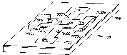
A Josephson junction device 100 ig shown in
Figure 1. The device as shown consists of a substrate
SUB. Located on the substrate is an underlying
superconductive crystalline oxide layer USCO confined
with a selected area defined by a boundary 1. A first
nonsuperconductive oxide layer portion lNSO overlies
the remainder of the upper surface of the substrate,
laterally abutting USCO along boundary 1.
An impedance controlling crystalline oxide
layer ICCO overlies a central portion of USCO. Located
on lNSO and laterally abutting ICCO are two second
nonsuperconductive oxide layer portions 2NSOa and
- 2NSOb. The lateral boundaries between ICCO and 2NSOa
and 2NSOb are along boundary 1. Therefore, ICCO is
entirely confined within the selected area while 2NSOa
and 2NSOb are entirely excluded.
An overlying superconductive crystalline
oxide layer OSCO overlies and is confined to the area
of ICCO. Located on and confined to 2NSOa and 2NSOb,
respectively, are third nonsuperconducting oxide layer
portions 3NSOa and 3NSOb. The lateral boundaries
between OSCO and 3NSOa and 3NSOb are along boundary 1.
Therefore, OSCO is entirely confined within the
selected area while 3NSOa and 3NSOb are entirely
excluded.
The overlying superconductive cry~talline
oxide layer OSCO, the impedance controlling crystalline
oxide layer ICCO, and the portion of the underlying
superconductive crystalline oxide USCO that underlies
OSCO and ICCO form a Josephson junction layer se~uence
that is capable of conducting electricity with no
measurable resistance under one condition of use and
.
. ~.. . . . .
.
,
::
'. ' :~ '
: '
2~3~
--8--
capable of switching to a nonsuperconducting mode ~hen
another condition is imposed.
For the Josephson junction layer sequence to
perform its intended active circuit function it is
essential that the device be constructed in a manner
that provides for circuit connection with minimal risk
to the operating characteristics of the device. In the
device 100 electrically conductive layers ECa and ECb
overlie 3NSOa and 3NSOb, respectively, and each extend
across the boundary 1 and overlie a portion of ~SCO.
ECa and ECb in extending laterally beyond the Josephson
junction layer sequence provide bonding pads BPa and
BPb, respectively, each at a location laterally remote
from the Josephson junction layer sequence. This
avoids subjecting the electrically active portion of
the device to the stresses characteristic of bond
attachrnent--e.g., any one or combination of pressure,
heat and ultrasound.
In extending the electrical conductors
laterally the underlying nonsuperconductive oxide la~er
portions provide an important role. In the absence of
lNSO, 2NSOa and 3NSOa extending ECa laterally from OSCO
would run the risk of contacting USCO and thereby
shuntin~ the impedance controlling crystalline oxide
layer ICCO. One valuable function which lNSO, 2NSOa
and 3NSOa play is then to eIectrically separate ECa
from USCO and ICCO. The same function is, of course,
also provided by the corresponding nonsuperconductive
layer portions underlying ECb.
A second valuable function which the
nonsuperconductive oxide layer portions underlying each
of ECa and ECb perform is to present these electrical
conductors with an essentially planar (flat or high
radius of curvature) supporting surface. Short radius
of curvature bends, such as those that would be
.
.
~'
- 9 -
required around the edge of OSCO in the absence of the
abutting nonsuperconductive oxide layer pGrtions, are
avoided. Short radius of curvature bends are sites
known to increase the rigk of el~ctrical conductor
discontinuities. They usually constltute sites of
maximum physical stress. Additionally, the essentially
planar nonsuperconductive oxide supporting surfaces for
the electrical conductors ECa and ECb reduce the risk
of electrical conductor discontinuities that can occur
at surfaces that are oriented at different angles. For
example, where ECa and ECb are formed by vapor phase
deposition techniques, such as sputtering, the
essentially planar nonsuperconductive oxide supporting
surfaces intended to receive ECa and ECb can be
entirely optimally oriented (e.g., oriented normal or
near normal) to the path of coating material. Whereas,
if any part of the supporting surfaces were oriented at
different angles, there is a risk of one or more
surface portions being less favorably oriented with
respect to the coating material source, resulting in a
thinned coating portion or ev~n a discontinuity, as can
be produced by shadowing effects. In actual device
manuEacturing the presence of the nonsuperconductive
oxide layer portion~ underlying the electrical contacts
ECa and ECb can be expected to result in increased
yields of high performance devices, thereby avoiding
the manufacture of devices that either fail or show
less than optimum performance capabilities.
As shown, a lateral gap 2 exists between
electrical conductors ECa and ECb. This allows
independent electrical addressing oE the ~osephson
junction layer sequence with each of ECa and ECb. It
is, of course, possible to simplify construction by
e}iminating ECb, 2NSOb and 3NSOb. In such instance ECa
'
'
. . . ~
,. ":
.. . .
--10--
is prefer~bly extended laterally to cover the entire
upper surface of the ~osephson junction layer se~uence.
The portions of ~SCO extending laterally
beyond the Josephson junction layer seguence within the
selected area defined by boundary 1 also provide
convenient laterally offset sites for electrical
conductor attachment. As shown, USCO is laterally
extended to provide bonding pads BPc and BPd. Thus,
the device, as shown, is provided with two sites for
electrical connection to USCO. It is recognized that
lateral extension to only one of PBc and BPd is
essential to providing a device satisfying the
requirements of the invention.
In practice lead attachments to BPa and BPc
can be used to complete a current conducting circuit
while separate leads can be attached to BPb and BPd to
complete a separate circuit or circuit portion intended
to monitor the voltage drop, i any, across the
Josephson junction layer sequence.
The device 100 has been shown as a discrete
single circuit element device. It is, however,
recognized that the device can be readily adapted to
accommodate hybrid or integrated circuit features. A
large portion of lNSO and the entire backside of the
substrate S are not occupied and can readily serve as a
supporting surface for other active or passive circuit
components.
Although the device 100 has been shown as
having a single Josephson junction active portion, it
is appreciated that the invention can readily
accommodate construction of devices having any numbar
of Josephson junction active portions electrically
isolated or connected in series or parallel on a single
substrate. When multiple circuit elements are formed
on a single substrate, instead of attaching leads at
,,
2 ~
each of the bondiny pads the geometrical pattern of the
area represented by one or more of the bonding pads c~n
be configured to provide a conduction path to an
adjacent device on the substrate.
Device 200, shown in Figure 2 and 3,
illustrates a device containing two Josephson junction
active portions electrically connected in series. The
substrate SUB' can be identical to that of device 100.
An underlying superconductive crystalline oxide layer
USCO~ can be identical to the corresponding layer in
device 100. As shown in device 200 USCO' is confined
to a first selected area indicated by boundary 3 (most
clearly illustrated in Figure 7). Laterally abutting
USCO~ along boundary 3 is a first nonsuperconductive
oxide layer portion lNSO~. Overlying USCO' at spaced
locations within the selected area defined by boundary
3 are two layers ICCOa and ICCOb each similar to ICCO
of device 100. In area 4 between ICCOa and ICCOb the
underlying superconductive crystalline oxide layer
USCO' is free of any overlying oxide. Overlying ICCOa
and ICCOb, respectively, are OSCOa and OSCOb, each
similar to OSCO of device 100.
Laterally abutting ICCOa and ICCOb along
boundary 3 is 2NSO' (similar to 2NSOa and 2NSOb), and
laterally abutting OSCOa and OSCOb along boundary 3 is
3NSO' (similar to 3NSOa and 3NSOb). As shown the
nonsuperconductive layer portions are each continuous
and laterally surround the boundary 3. The upper
surface of 3NSO' forms an essentially planar lateral
extension of the upper surfaces of OSCOa and OSCOb.
Therefore, essentially planar surfaces are provided for
ECc and ECd which extend from OSCOa and OSCOb laterally
over a portion of 3NSO~ to laterally offset bonding
pads BPe and BPf, respectively. Not only is an
essentially planar surface provided for formation of
. ' :. . . ` ~ .
~'
~ ,
-12-
ECc, ECd, BPe and BPf, but a large additional area of
3NSO' remains unoccupied surrounding the boundary 3
that is available for construction oE other circui~
elements, if desire~. Haviny all of the u~per Yur~aces
of the device, except for a relatively small area 4,
lying in essentially the same plane is, of course,
recognized to be highly advantageous for circuit
construction for the reasons provided in describing the
features of device 100.
In constructing Josephson junction devices
100 and 200 a common starting point, shown in Figure 4,
is a substrate SUB~ bearing a Josephson junction layer
sequence 5, which, as shown, consists of an underlying
superconductive crystalline oxide layer USCO" located
on the substrate, an impedance controlling crystalline
oxide layer ICCO", and an overlying superconductive
oxide layer OSCO". The substrate can take any
conventional form known to be capable of supporting the
formation of a high temperature superconductive
crystalline oxide layer. Initially the Josephson
junction layer sequence extends laterally beyond the
Josephson junction layer sequence boundaries of the
completed device. It is usually most convenient for
the Josephson junction layer sequence as initially
formed to overlie the entire upper surface of the
substrate.
The Josephson junction layer sequence can be
chosen to be either the S-I-S or S-N-S type. In this
invention S in each occurrence represent~ a high
temperature superconductive ~To ~ 30 K) crystalline
oxide. More specifically, USCO~ i~ one oE the S layers
while OSCO" is the other.
ICCO~ layer can take the form of either an I
or an N layer. To complete an S-I-S layer sequence
ICCOI~ must be formed of an electrically insulative
: .
'
, ' '
.
3l3f~
material having a bulk re.sistivity in the order of 101
ohm-crn or higher. Addition~lly, in it~ I form ICCOn
must have a thickness of at least ~ crystal lattice
monolayer (e.g., at least 5A). ICCO" preferably ha~ at
thickness of less than 30A, but with decreasing levels
of resistance ICCOn can be increased up to loOA in
thickness. In an ideal S-I-S Josephson junction layer
sequence ICCO" is believed to support superconductivity
in its low impedance state primarily by permitting
tunneling of paired electrons (Cooper pairs), which are
the recognized charge carriers in superconductive
structures.
Unlike S-I-S layer sequences, when ICCOa
completes an S-N-S layer sequence, superconductivity
through the ICCO" layer in its low impedance state
cannot be explained by current theories of tunneling
behavior. S-N-S layer sequences are said to rely on
experimentally verified, but theoretically less well
understood "proximity effects" to support
superconductivity. To achieve a proximity effect
capable of supporting superconductivity at a
temperature of greater than 30 K the bulk resistivity
of the material forming layer ICCO~ is greater than
10 6 ohm-cm and is preferably greater than 10 3 ohm-cm.
In addition ICCO~ must have a thickness of less than
10,000 Angstroms, preferably less than 5000 Angstroms,
and optimally less than 100 Angstroms. Where proximity
effects rather than tunneling are being relied upon for
superconductivity in ICCOU, it is usually convenient to
fonm ICCO" with a thickness of at least about 10
Angstroms.
Regardless of whether the Joseph~on junction
layer sequence 5 is characterized as S-I-S or S-N-S,
the layers USCO", ICCO" and OSCO" are each crystalline
oxide layers. Since layer ICCO" must be quite thin, it
.. . ~. . .
.~. ~ ,
.
'
.,
important that the underlying high ter~eratu~e
superconductive oxide layer USCO~ present a smooth
surface for deposition of ICCO~. Surface
irregularities on USCO~ are most conveniently minimized
by constructing USCO~ as a thin film. As employed
herein the term ~thin filmn is ernployed to indicate a
layer thickness of less than 5 ~m. Preferably USCO~
has a thickness of less than 1 ~m.
Successful device construction also depends
on not unduly restricting the thickness of layer USCOn.
Device layers USCO and USCO~ that are formed from USCO~
must be thick enough to conduct current laterally from
the active area of the Josephson junction devices 100
and 200 without exceeding the critical current density
of the superconductive crystalline oxide from which
they are formed. Additionally, at a subsequent stage
in the processing, described below, overlying oxide
layers must be removed while leaving USCO and USCO'
- intact. The layer USCO~' must be thick enough to allow
for some thinning as a way of insuring complete removal
of the overlying oxide layers. For USCO and USCO' each
to have a thickness of at least 500 Angstroms USCO~
must have a thickness greater than 500 Angstroms. In
an optimum construction USCO and USCO' each have a
thickness at least 5000 Angstroms, and USCO~ has a
thickness of greater than 5000 Angstroms.
For reasons that will become apparent from
subsequent description of the process of preparation,
all of the superconductive crystalline oxide layers of
the Josephson junction layer sequence are contemplated
to be thin films. As herein employed, the term ~thin
film~ indicates a thickness of less than 5 ~m.
Preferably, none of the superconductive crystalline
oxide layers exceed 1 ~m in thickness.
,`
.
.
-- ,
` '
3 ~
-15-
After the underlying superconductive
crystalline oxide layer USC'O" is ~ortned on the
substrate, the impedance controlliny c~rys~alline oxide
layer ICCO" is epitaxially grown over USCO~. During
epitaxial growth the crystal orientation of -LCCO~ is
controlled by that of USCOn. Similarly, once formed,
ICCO" provides a deposition surface for the epitaxial
growth of the overlying superconductive crystalline
oxide layer OSCOn. It is an important and highly
advantageous feature of this invention that USCOR,
ICCO" and OSCO" can each be formed in rapid succession,
optimally in t~e same controlled environment, without
any intervening device fabrication steps being
re~uired. This avoids any risk of degrading the
exposed upper surfaces of layers USCO" or ICCO" during
formation of the layer sequence and thereby degrading
either the purity or crystal structure of ICCO" or
OSCO" as they are subsequently formed.
- Since layer OSCO" need not serve as a
substrate for further crystalline oxide deposition and,
unlike layer USCO~, need not support current conduction
laterally to any appreciable extent, even ~hinner layer
thicknesses are possible than in constructing layer
USCO". OSCO" need not serve as a substrate for further
epitaxial deposition, and therefore, unlike the
formulation of USCO", this is not a consideration for
limiting its thickness. However, since thickening
OSCO" increases the amount of material that must be
subsequently removed in device preparation, it is
` 30 preferred to construct OSCO" as a thin ~ilm. Any
; minimum thickness of OSCO~ capable of insuring a
continuous film can be employed. It is generally
preferred that OSCO" having a thickness of at least
about 0.1 micrometer. It is usually convenient to form
USCO" and OSCO~' within the same thickness ranges.
, .
~ .,
-16~
Once the ~osephson junction la~er se~uerlce is
formed on the substrate the next ste~ in device
fabrication is to convert the portiorl of the layer
se~uence lying outside a selected are~ to a
nonsuperconductive form, preferably an insulative form
(i.e., a form having a bulk resistivity of at least
101 ohm-cm). This is accomplished by first protecting
the ~osephson junction layer sequence in the selected
area. In forming the device 100 the selected area is
defined by boundary 1 in Figure 5, and in forming the
device 200 the selected area is defined by boundary 3
in Figure 7. With the selected area protected, the
remaining, unprotected portion of the Josephson
junction layer sequence is converted to a
nonsuperconductive form. This can be accoT~plished, ~or
example, by bombarding the unprotected surface of the
Josephson junction layer sequence with ions capable of
entering the unprotected crystalline oxide layers and
- converting these layers to a nonsuperconductive and,
preferably, an insulative form. Ions implanted by
bombardment can be either those that by their presence
inhibit superconductivity (i.e., convert the layers
from a superconductive to a nonsuperconductive
composition), those that destroy the crystal structure
essential to support superconductivity without
introducing ions that are incompatible with
superconductivity, or those that achieve a combination
of both effects. It is preferred to use ions that are
not incompatible with superconductivity to de~troy the
crystal structure that supports superconductivity
(i.e., to convert the superconductive crystalline
oxides to nonsuperconductive, preferably insulative,
amorphous oxides), since this avoids any possibility of
subsequent device degradation by migration of
incompatible ions into the selected active area of the
~ .
~; ~
2~ 3 3
-17-
device. Koch et al, ~'Quantum Interference Devices Made
from Superconducting Thin Films", Appl. Ph~s. Lett.
~1(3), July 20, 1987, pp. 200~202, cited abo~e and here
incorporated by reference, reports conversions of the
type contemplated by oxygen bombardment at an energy o
0.25 to 1 MeV and a dose of 1014 to 5 X 10¹⁵ ions/cm2
or arsenic bombardment at an energy of 1 to 2.5 ~eV and
a dose of 1014 to 5 X 10¹⁴ ions/cm2. O~ygen, silicon
and gold ions are preferred for implantation. It is,
of course, appreciated that overall thickness of the
Josephson junction layer sequence 5 must be small
enough to permit ion penétration of each of layers
OSCO", ICCO~ and OSCO". This is another reason for
forming these layers of a minimum acceptable thickness.
The selected area can be protected from
conversion to a nonsuperconductive form by any
convenient conventional technique. In a preferred fonn
of the invention one or a combination of period 5
and/or ~ metals are coated to overlie the selected
area. Tantalum, tungsten, platinum and gold coated to
a thickness of from 0.5 to 2.0 ~m are examples of
period 6 metal layers. Period 5 metals, such as
palladium and silver, are effective at about twice the
layer thickness of period 6 metals. One or more
; 25 lighter metals can be mixed with or underlie the period
5 and/or 6 metals to facilitate protective layer
formation and adhesion. A preferred layer combination
is a chromium layer overcoated with a period 6 metal,
where chromium is relied upon to improve the adhesion
of the period 6 metal layer. Since no portion of the
protective layers need form a part of the completed
device, it is preferred to interpose an underlying
~ layer, such as a photoresist layex, that facilitates
`~ lift off after conversion of unprotected portions of
the ~osephson junction layer se~uence to a
,'~
.
-18~
nonsuperconductive forrn. A ~pec~ieic step se~uence f~r
forming, patterning and later rerhoving a prote~tive
layer is set out in the Examples.
At the completion of the ion bornbardment step
the Josephson junction layer sequence 5 remains intact
within the selected areas defined by boundaries 1 and 3
while the portions of the originally deposited
Josephson junction layer sequence laterally surrounding
and laterally abutting (contiguous to) the boundaries 1
and 3 are converted to nonsuperconductive oxide layer
portions. Because of the disruptions of the original
crystal structure by ion bombardment the
nonsuperconductive oxide layer portions may or may not
remain distinguishable as separate layers. ~or
example, if USCO", ICCO~ and OSCOU are all of the same
initial composition and differ only in their crystal
structure, it is apparent that when the portions of
these layers outside the selected area are converted to
an amorphous form by ion bombardment nonsuperconductive
oxide portions lNSO, 2NSOa, 2NSOb, 3NSOa and 3NSOb in
device 100 and the corresponding layer portions in
device 200 may be indistinguishable in composition.
Instead of relying on ion implantation to
create a nonsuperconductive oxide layer portion
occupying the entire area exterior of the selected
areas defined by boundaries 1 and 3, it is
alternatively possible to define the selected
boundaries 1 and 3 using a laser to convert the
boundary abutting portions of the Josephson junction
layer sequence to a nonsuperconductive for~. This
technique is described by Hayashi et al U.S. Patent
4,891,355, cited above.
In constructing the device 100 the next step
of the process is to coat the upper surface of the
intermediate workpiece having the appearance shown in
' ~
J.
: `
2 ~jC)~3~
--19--
Figure 5 with the electrical conductor (e.g., metal or
metals) intended to form ECa and ECb The electrical
conductor can be coated ln only the areas of ECa and
ECb or those areas and any additional area, except area
2. In practice it is usually most convenient to coat
the electrical conductor uniformly over the upper
surface of the workpiece in two areas laterally
separated by the width of area 2. Since in one fo~n of
the invention ECa and ECb can toyether form a single
electrical conductor, it is appreciated that, if
desired, the electrical conductor can be simply coated
over the entirç upper surface of the workpiece.
In forming the device ~00 electrical
conductor used to form ECc and ECd is preferably coated
in a pattern either confined just to areas ECc and ECd
or just those areas and area ~. The purpose of
patterning the electrical conductor at this stage of
- processing is that, unlike the fabrication of device,
removal of unwanted oxide layer portions in subsequent
2Q steps does not simultaneously produce the electrical
; conductor pattern. Therefore, prior patterning offers
better protection against inadvertent contamination of
underlying layers than deferrin~ patterning until
unwanted portions of the oxide layers have been
removed.
The next step in the preparation process is
to remove portions of the crystalline oxide layers
overlying USCO and USCO'. In constructing the device
100 this is accomplished by forming a patterned
photoresist layer PR occupying only the areas of ECa, 2
and ECb, as shown in Figure 6. In constructing the
` device 200 this is accomplished by forming a patterned
photoresist layer PR' occupying the entire upper
surface of the workpiece, except area 4, as shown in
Figure 8.
,
2 ~ ~ ` J ~
--~0--
With the photoresist patterned the portions
of the oxide layers not protecte~ by P~ or PR' are
removed to a depth sufficie~t to reveal the upper
surface of the underlying superconductive oxide layer
USCO or USCO'. While liquid etchants ca~ in theory be
used for oxide removal, it is preferred to employ ion
milling. Ion milling offers advantages in that the
risk of contamination of the superconductive layers
remaining by liquid impurity ions is avoided, better
pattern definition is realized, no chemical degradation
along edges is produced, and etch rates are more
uniform. Any conventional procedure for ion milling
known to be useful in patterning superconductive
crystalline oxides can be employed. The technique of
Heijman U.S. Patent 4,933,318, cited above, is
specifically contemplated.
Upon completion of ion milling the
photoresist is removed with a suitable solvent. After
this step the devices 100 and 200 are in the forms
shown in Figures 1 and 2, respectively. The devices
can be put to direct use as shown or further processed,
such as by formation of other circuit components on
lNSO, 3NSO', SUB or SUB', lead attachment, passivation
or encasement, by conventional procedures that form no
part of this invention.
The substrates, the high temperature
superconductive crystalline oxides and the Josephson
layer sequences employed in the practice of this
invention can take any convenient conventional form. A
wide variety of high temperature superconductive
crystalline oxides are available, as illustrated by
Shappiro et al U.S. Patent 4,940,693 and Itozaki et al
U~S. Patents 4,942,142 and 4,942,152, cited above.
: Generally any substrate and high temperature
superconductive crystalline oxide known to produce a
,
thin film on the substrate can be employed in
combination. Examples of such combinations a~ well as
processes of depositing the thin film on the substrate
are provided by Mir et al U.S. Patent 4,880,770;
~oinuma et al U.S. Patent 4,902,671; Wu U.S. Patent
4,929,595; Yamaoki et al U.S. Patent 4,935,403;
Nishiguchi et al U.S. Patent 4,g37,226; Collins et al
U.S. Patent 4,960,753; Gallagher et al U.S. Patent
4,962,086; Fujita et al U.S. Patent 4,925,829; Kimura
et al U.S. Patent 4,931,425. Laser ablation deposition
has been demonstrated by Shaw et al U.S. Patent
4,874,741; Dijkkamp et al ~Preparation of Y-Ba-Cu Oxide
Superconductor Thin Films Using Pulsed Laser
Evaporation From High Tc Bulk Material~, App. Phys.
Lett. 51~8), 24 Aug. 1987, pp. 619-621; and Wu et al
~Superlattices of Y-Ba-Cu-O/Yy-Prl_y-Ba-Cu-O Grown by
Pulsed Laser Deposition", Appl. Phys. Lett. 56(4), 22
Jan. 1990, pp. 400-402; each cited above. While any
conventional procedure can be employed for deposition
- 20 of ~he high temperature crystalline oxide thin films,
preferred techniques of deposition, particularly for
the impedance controlling and overlying superconductive
crystalline oxide layers, are sputtering, laser
ablation and vacuum vapor deposition, since each of
these techniques can be accomplished without bringing
the substrate or layers into contact with a liquid
during preparation.
The substrate and ~osephson junction layer
sequences of Rogers et al, UFabrication of
Heteroepitaxial YBa2cu3o7-x-prBa2cu3o7-x-yBa2cu3o7-x
Josephson Devices Growr. by Laser Deposition~, Appl.
Ph~s. Lett. ~(19), Nov. 6, 989, pp. 2032-2034;
- Yamazaki U.S. Patent 4,916,116; and Johnson et al U.S.
Patent 4,933,317; each cited above, are specifically
contemplated for use in the practice of this invention.
" ~3 J3 j~J
-22-
In a specifically preerred form of the
invention the ~osephson junction laye~ s~quence 5 o
Figure 4 is constructed so that the ~hin filrn high
temperature superconductive crystalline o~ide layers
USCO~ and OSCO" exhibit an RlA2C3 orthorhombic
perovskite crystal structure while the layer ICCOR
exhibits a cubic perovskite crystal structure. The
substrate SUB" can take any convenient form capable of
permitting deposition of USCO~ thereon as a thin film.
In a specifically preferred form of the
invention SUB" is chosen from materials that themselves
exhibit a perovskite or perovskite-like crystal
structure. Strontium titanate is an example o~ a
perovskite crystal structure which is specifically
preferred for use as a substrate. Lanthanum aluminate
(LaAl03), lanthanum gallium oxide (LaGaO3) and
potassium tantalate are other examples of useful
perovskites. Other preferred substrates which are not
perovskites include magnesia and alumina, particularly
in their monocrystalline forms.
When the substrate includes one or a
combination of barrier layers to serve as the
deposition surface for USCO", it is recogniæed that a
much broader choice of substrate materials are
possible. Illustrations of substrates containing one
or more barrier layers for the deposition of thin film
high temperature superconductive oxide crystalline
oxides are provided by Mir et al U.S. Patent 4,880,770;
Agostinelli et al U.S. Patent 5,017,551; Hung et al
U.S. Patent 4,908,348; and Agostinelli et al U.S.
Patent 4,956,335. Barrisr layers are particularly
useful when the substrate takes the form of
monocrystalline semiconductor, such as a silicon or
III-V monocrystalline semiconductor. Specifically
contemplated examples of the latter are yttrium or
.
2 n ~ 9
-23-
calcium stabilized zirconia barrier layers on
monocrystalline silicon or gallium ar~erlide substrates
or alkaline earth (e.y., barium or strontium) fluoride
barrier layers on monoc~ystalline silicon or gallium
arsenide substrates.
The thin film high temperature
superconductive crystalline oxide layers USCO~ and
OSCO~' in a specifically preferred form of the invention
exhibit an RlA2C3 orthorhombic perovskite crystal
structure that satisfies the relationship:
(I)
RlA2C307 -W
where
R, A and C represent rare earth, alkaline earth
and copper atoms, respectively, capable of forming a
high temperature superconductive RlA2C3 orthorhombic
perovskite crystal structure and
w is in the range of from 0.5 to 0, preferably 0.3
to 0 and optimally from 0.1 to 0.
Progressively higher temperatures of superconductivity
can be realized as the value of w is decreased.
The cubic perovskite crystal structure that
forms ICCO" in its specifically preferred form
satisfies the relationship:
(II)
Ro.33+zA0.67cl-yO3-x
where
R, A and C represent rare earth, alkaline earth
and copper atoms, respectively, capable of forming a
superconductive RlA2C3 orthorhombic perovskite crystal
structure;
x is 0.67 to 1;
y is 0 to 0.2; and
.
;'' . `
2 ,~ 3 . ~ ~
-24-
z is 0 to 0.1.
When compaxing a cubic perovskite unit cell
structure to that of a superconductive RlA2C3
orthorhombic perovskite crystal structure unit cell,
certain similarities and differences are apparent. One
of the most important similarities is that the cubic
perovskite unit cell exhibits dimensions that are
similar to the minor axes dimensions of an RlA2C3
orthorhombic perovskite unit cell formed of the same
elements. Similarities in both unit cell facial
configuration and dimensions facilitate epitaxial
deposition of either crystal structure on the other.
The cubic perovskite unit cell structure can
contain oxygen in the same proportions found in a
corresponding RlA2C3 orthorhombic perovskite crystal
structure. In a preferred form of the invention x is
in the range of from 0.~7 to 0.85.
The orthorhombic perovskite unit cell
structure 1:2:3 atomic ratio of rare earth:alkaline
earth:copper can be present in the cubic perovskite
unit cell structure. A slight excess of rare earth can
be present in the preferred cubic crystal structures.
In preferred cubic perovskite crystal structures z
ranges from zero to 0.08. The cubic perovskite crystal
structure as a bulk material does not exhibit
superconductivity at temperatures at or above 30C--
i.e., at contemplated device operating temperatures,
and thus satisfies a general material requirement for
use as an ICCO device layer.
Any combination of rare earth, alkaline earth
and copper elements known to be capable of forming a
superconductive RlA2C3 orthorhombic perovskite crystal
structure is contemplated for forming the USCOa, ICCO"
and OSCO" layers of the Josephson junction devices of
the invention. The term "rare earth" is used to
:
. ~
~` .
~::
2 ~ ~ f,,~
-25-
indicate group 3, periods 4, 5 and 6 elements.
Scandium, yttrium and the lanthanide~, other t~an
- cerium, praseodymium, promethium and terbium (i.e., the
lanthanides neodymiurn, samarium, europium, gadolinium,
dysprosium, holmium, erbiurn, thulium, ytterbium and
lutetium), employed singly or in combination, are known
to produce superconductive RlA2C3 orthorhombic
perovskite crystal structures. Yttrium and the above-
identified lanthanides constitute specifically
preferred rare earths. The alkaline earth elements are
preferably at least 50 percent barium on an atomic
basis with any additional alkaline earths being chosen
from the group consisting of strontium and calcium,
most preferably at least 80 percent barium on an atomic
basis with the additional alkaline earth element, when
present, being strontium.
A specifically preferred orthorhombic
perovskite crystal structure satisfies the unit cell
formula:
(III)
7_w
where
w is in the range of from 0 to 0.3, preferably
0.1 .
A specifically preferred cubic perovskite
crystal structure satisfies the unit cell formula:
(IV)
. 33~ZBaO . 67CUl-y3-x
where
x represents 0.67 to 0.85;
y represents 0.05 to 0.18; and
z represents up to 0.08.
. .
.' ,~
~ ~ r, ~3 :
--26--
This unit cell Eormula is highly compatible with high
To YlBa2Cu3 crystal structur~s.
The cubic perovskite crystal structures
employed in the practice of this i~vention are novel.
They can be produced by varying the conditions employed
for forming RlA2C3 orthorhombic perovskite crystal
structures by the laser ablation deposition process.
For example, novel cubic perovskite crystal structures
can be produced by varying temperatures employed in the
laser ablation deposition processes disclosed by
Dijkkamp et al ~Preparation of Y-Ba-Cu Oxide
Superconductor Thin Yilms Using Pulsed Laser
Evaporation From High ~c Bulk Material", Appl. Phys.
Lett. 51 (8), 24 August 1987, pp. 619-621; Wu et al
"Superlattices of Y-Ba-Cu-O/Yy_Prl_y-Ba-Cu-O Grown by
Pulsed Laser Deposition", Appl. Phys. Lett. 56 ~4), 22
January 1990, pp. 400-402; and Rogers et al
~Fabrication of Heteroepitaxial YBa2Cu3O7_x-PrYBa2_
CU37-x~YBa2Cu3O7-x Josephson Devices Grown by Laser
Deposition, Appl. Phys. Lett. ~ (19), 2 November 1989,
pp. 2032-2034.
In the laser ablation deposition process any
rare earth alkaline earth copper oxide having the rare
earth, alkaline earth and copper stoichiometry of a
superconductive RlA2C3 orthorhombic perovskite crystal
structure can be used as a source material. The source
material can be either crystalline or amorphous. The
source material is placed in an evacuated chamber
adjacent a heated stage on which is mounted a
substrate. The substrate is mounted in thermally
conductive contact with the heated stage. The accepted
and most replicable practice (here adopted) is to
monitor and regulate the temperature of the heated
stage. A series of laser pulses aimed at the source
material is responsible for transfer of material from
.
. ,
k ~
-~7~
the bulk source to the substrate. During abl~tion a
plasma is created containing a mixture of rare earth,
al~aline earth and copper elements and ion~. These
elements interacting with oxygen condense on the
substrate to reform a rare earth alkaline earth copper
oxide. In addition to its simplicity, the process has
the advantage that high vacuum conditions are not
required, although they can be employed. For example,
ambient pressures ranging from 1.33 X 10 2 to 400 Pa
` 10 (10 4 to 300 mtorr) have been reported.
It has been discovered that by maintaining
the temperature of the heated stage below ~but
typically within about 120C of) the temperature
required to produce an RlA2C3 orthorhombic peravskite
crystal structure a coating of a cubic perovskite
crystal structure is formed on deposition. A preferred
temperature range for formation of the cubic perovskite
crystal structure is in the range of from about 530 to
640C. For yttrium barium copper oxide deposition in a
cubic perovskite crystal structure an optimum
temperature range is from 540 to 630C.
A specific advantage of forming USCO" and
OSCO" of a single orthorhomhic perovskite crystal
structure and ICCO" of a cubic perovskite crystal
structure using the same rare earth and alkaline earth
elements and the same 1:2:3 atomic ratio of rare
earth:alkaline earth:copper is that all three layers
can be formed in a single vacuum deposition sequence
using a single laser ablation target. This greatly
simplifies construction of the Josephson junction layer
sequence and assures producing high quality surfaces in
the underlayers USCO" and ICCO" for epitaxial
deposition of layers ICCO" and OSCO", respectively,
thereon. The fact that the orthorhomic perovskite
crystal structure and the cubic perovskite crystal
. .
~2~
structure can each consist of the ~ame elements in the
same ratios minimizes any risk of impurity ion
degradation of the ~osephson junction layer se~u~nce
and enhances the epitaxial compatibility of the layers.
The ~osephson junction devices of the
invention lend themselves to a variety of uses. The
devices of the invention can be used to switch from no
measurable resistance at a low current density to a
higher, measurable resistance at a higher current
density. It is also contemplated to employ the
Josephson junction devices of the invention as sensors.
In one contemplated construction the ~osephson junction
device is biased to a region in its current-voltage
hysteresis loop in which the ratio of current change to
voltage change (~I/AV) is a maximum. When so biased,
a small amount of heating of the Josephson junction
layer sequence can produce a marked change in current.
The heat can, if desired, be supplied to the device in
another conveniently transmitted energy form, such as
ultrasound or electromagnetic radiation, and converted
to heat by absorption. In an alternative mode of
operation electromagnetic radiation of an energy level
capable of dissociating Cooper pairs (the paired
electrons that support superconductivity), preferably
electromagnetic radiation exhibiting a frequency of at
least 1 terrahertz, can be directed to the impedance
controlling layer. In this mode the electrical
conductors (E~a-d) at least in the areas overlying the
Josephson junction layer sequence are preferably formed
of material that is relatively transparent to the
electromagnetic radiation to be sensed. For example,
if the electromagnetic radiation i8 light, the
electrical conductors in their preferred form can
conveniently be formed as a conductive transparent
:, :
,
,: . '
-~9
metal oxide, such as indium oxide, tin oxide or, mo~t
preferably, indium tin oxide.
~E
The invention can be further appreciated hy
reference to the following specific examples. The term
~m~ signifies micrometers. The acronyms "XRDR and
~TEMn stand for X-ray diffraction and transmission
electron microscopy, respectively.
Example 1 Cubic Perovskite Crystal
Structure Thin Film on MgO
The title film was deposited on a {100
crystal face of a monocrystalline magnesia (MgO)
substrate by laser ablation deposition.
The target material was a 2.54 cm diameter
disk of bulk polycrystalline YBa2Cu3O7_x high
temperature superconductor material. The target was
mounted on a rotating stage and positioned in a vacuum
chamber. During deposition the target rotation rate
was 6 rpm.
The monocrystalline MgO substrate was 2.5 X
1.3 cm and was located on a resistively heated stage 5
cm from the target. The MgO substrate was mounted on
the heated stage using spring clips and a silver paint
thermal transfer layer between the heated stage and the
substrate to facilitate efficient heat transfer. The
substrate was preheated on the stage prior to
deposition both to pyrolyze the paint vehicle and to
clean the substrate surface of any organic residues.
During this step the substrate heater block was raised
to 700C and held at that temperature for 5 minutes.
The chamber was then pumped to a pressure of
6.7 X 10 2 Pa (5 X 10⁻⁴ torr) and then backfilled while
pumping with oxygen to a pressure of 26.7 Pa ~200
mtorr) measured 20 cm away from the target. The oxygen
:.
.
~i3 J ,~ 3
-30-
was introduced via a tube which directed the gas toward
the substrate surface. T~le oxy~en flow r~te was
controlled at 20 sccm.
A 2~8 nm laser beam from a Lambda Physik
210iTM (KrF) excimer laser was directed on the target
via a highly reflective mirror, a 500 mm high purity
fused quartz lens and vacuum chamber window of a
similar quartz material. The laser was operated at a
repetition rate of 2 Hz with a pulse duration of about
20 ns and a pulse energy of 400 mJ. The beam spot size
on target measured about 2.5 X 8 mm, ~iving a fluence
near 2 J/cm2.
A shutter interposed between the target and
substrate was closed to permit the target to be laser
addressed without depositing material on the substrate.
The laser was fired for 150 pulses i~mediately before
opening the shutter to insure that the highest possible
purity of material was made available from the target.
With the shutter opened, a total of 3000
laser pulses were used to grow the film on the
substrate. During deposition the heated substrate
stage was maintained at 560C. After the 3000 laser
pulses the oxygen pressure in the chamber was raised to
about 22.7 kPa (170 torr). The sample was maintained
in this environment for 15 minutes, after which heating
of the substrate stage was discontinued. The sample
was allowed to cool to room temperature and then
removed.
The deposited film was found to have a shin~
black appearance. Room temperature four point probe
resistivit~ measurements gave a sheet resistance of
about 100 ohms per square. The film thickness was
found to be approximately 3000 Angstroms by
profilometry. XRD showed the film to be a highly
ordered cubic crystal structure presenting a ¢lOOJ
2 ~
-31-
crystallographic surface. XRD and T~M analyses of this
and similarly prepared samples analy~i~ also indicated
a very thin interfacial RlA2C3 orthorhombic perovskite
crystal structure, indicating that the fir~t few unit
cell lattice planes exhibited the RlA2C3 orthorhombic
perovskite crystal structure before ~ormation of the
cubic perovskite c~ystal structure began.
Example 2 Cubic Perovskite Crystal
Structure Thin Film on SrTiO3
A thin film was prepared similarly as
described in Example 1, except that a monocrystalline
SrTiO3 substrate was substituted for the MgO substrate.
Deposition was undertaken onto a {100} crystal face.
The cubic perovskite crystal structure thin
film produced was similar to that observed in Example
1, but with the difference that no orthorhombic
perovskite crystal structure was detected by XRD
analysis. Ion channeling measurements indicated a
significant degree of crystalline perfection, with an
aligned minimum backscatter yield of 71~.
Example 3 The Effect of Temperature on
Obtaining Orthorhombic or Cubic Perovskite
Crystal Structure Thin Films on MgO
Except as otherwise noted, the procedure
employed was similar to that of Example 1. The heated
substrate stage temperature was held at 700C during
deposition. A total of 1500 laser pulses were used to
grow the film. The introduction of oxygen at the
conclusion of the run occurred with the heated
substrate stage temperature maintained at 700C. The
heated stage was then cooled at controlled rate,
reaching 200C after 90 minutes. At this point, the
supply of heat to the substrate stage was discontinued,
and the substrate was allowed to cool.
.,
~ ,
. , , . ~
:
2 i~
-32-
The thin film had a sh.iny black appearance,
XRD analysis revealed it to a highly oriented YlBa2Cu3
orthorhombic perovskite crystal ~tructuxe with the unit
cell c-axis normal to the substrate surface.
Superconductivity (To) was observed at 86C.
The significant difference between the
procedure of Example 1 resulting in a cubic perovskite
crystal structure and the procedure described above
resulting in an orthorhombic perovskite crystal
structure was that in Example 1 the temperature of the
heated stage (and therefore the substrate) was
maintained at 560C during deposition, whereas in the
procedure described above the ternperature of the heated
stage during deposition was 700C.
During further investigations the following
relationships between the heating stage temperature
during deposition and the observed thin film crystal
structure were observed:
Table I
20Heat Sta~e (~Çl Thin Film Crystal EQ~m
: 525 Amorphous
550 Cubic Perovskite
: 625 Cubic Perovskite
650 Orthorhombic Perovskite
At temperatures in the range of 525 to 550C a mixture
of amorphous and cubic perovskite phases were observed.
At temperatures in the range of 625 to 650C
indications of a mixture of cubic and orthorhombic
perovskite phases were observed.
30 . Example 4 Thermal Stability of Cubic
Perovskite Thin Films
A cubic perovskite thin film similar to that
of Example 1 was heated to 700C and then examined by
~, . .
.. ,. :
.: .:
.: , . :
,: ~ : .
-33-
TEM analysis. No evidence of conversion to an
orthorhombic perovskite crystal structure was ob~erved~
When a procedure analogous to that described
above was repeated, but with heating to 800C being
undertaken and XRD analysis being employed, no evidence
was found of the cubic perovskite crystal structure
being converted to an orthorhombic perovskite crystal
structure.
Example 5 Layer Arrangement for
Josephson Junction Structure
This example demonstrates the formation of a
three layer sequence of the type required for the
formation of a Josephson junction structure.
Except as otherwise indicated the procedure
of Example 1 was followed. The oxygen pressure during
deposition was 26.7 Pa (200 mtorr), and the laser pulse
energy was 350 m~. A first layer was formed using a
700C heated stage and 800 laser pulses, giving a first
layer thickness of about 800A. This layer exhibited an
orthorhombic perovskite YlBa2Cu3 unit cell crystal
structure similar to that described in Example 3. The
second layer was a cubic perovskite crystal structure
having a thickness of about 200A. The second layer was
similar to the thin film produced in Example 1. The
third layer was formed similarly to the first layer
with similar results.
XRD analysis of the resulting three layer
thin film suggested the presence of both the
orthorhombic and cubic perovskite phases. Ion
channelling measurements using 3.45 Mev He ions
indicated a high degree of crystalline perfection
throughout the film. Minimum backscattering yields of
73 percent at the surface and 45 percent near the
interface with the substrate were found, indicating a
higher degree of crystal perfection nearer the
. ~ ~
.
:
.. . .
-3~-
substrate interface and an epitaxial relationship of
layers throughout the film,
Example 6 Josephson ~unction Device
Construction
As specifically described below, a thin film
Josephson layer se~uence was deposited on a magne~ium
oxide substrate surface. YBa2cu3o7-w was chosen to
form the high temperature superconductive crystalline
oxide layers USCO" and OSCO" while the layer ICCO~ was
- 10 formed of a cubic perovskite crystal structure
- containing the same metal atoms in the same atomic
ratio. The Josephson junction layer sequence (and
hence the individual superconductive layers) exhibited
superconductivity at temperatures well above 30K and a
critical temperature estimated to be 90K. The entire
Josephson junction layer se~uence was deposited in a
single vacuum pumpdown using a single laser ablation
target.
A step-by-step description of device
preparation and testing follows:
A. Formation ~f ~h~ ~Q~Q~hSQ~
JunctionLay~r Se~uence
A polished 2.54 cm X 2.54 cm X 0.10 cm {100}
surface of a monocrystalline magnesium oxide wafer was
used as a substrate. The wafer was mounted on a
resistively heated block within a vacuum deposition
chamber. Silver paint was used as a heat transfer
agent between the heater block and the substrate. The
substrate was initially heated to 700C in air. The
deposition chamber was then pumped to a base pressure
of 1.33 X 10 6 kPa ~10 5 torr). Next, flowing oxygen
was introduced into the chamber near the substrate
while pumping continuously. A flow rate of 30 cc/min
, -. : ,. . - . -
: . :, ., .
:-
.
.:
:: :
.
. .
2 ~ ~ s~
~35~
and an oxygen pressure of 2.~ X 10-~ kPa (150 m~orr)
was established.
I'he substrate location wa3 5 crn from a
polycrystalline YBa2Cu3O7_w (w ~ 0.1) tar~et in a
direction perpendicular to the target surface. The
polycrystalline target was prepared using a
conventional technique (see Shaw et al U.S. Patent
~,874,741). The target was rotated at 6 rpm so that
laser exposure would strike different surfaces and
average out any local nonuniformities in the target.
With a shutter introduced between the target and the
substrate 150 pulses from a Lambda Physik model 210 i
(trademark) laser operating in the 248 nm KrF line were
made to irradiate the rotating target. Each pulse was
characterized by an energy of about 400 mJ and duration
of about 30 ns. The spot size on target was 3 mm by 10
mm. The laser was operated at a repetition rate of
Hz.
The shutter was then retracted, and, with the
substrate heater at 700C, an oxide precursor of a high
temperature superconductive crystalline oxide thin film
having an orthorhombic perovskite crystal structure was
deposited on the substrate using 7500 pulses. Next the
heat block temperature was lowered to 560C and 300
pulses were fired. These 300 pulses resulted in the
epitaxial deposition of an cubic perovskite interlayer
on the superconductive thin film. At this point the
substrate temperature was brought back to 700C and a
third layer was epitaxially deposited using 1500 pulses
as a precursor of an orthorhombic perovskite high
temperaturate superconductive crystalline oxide thin
film. For each layer a growth rate of approximately lA
per pulse was observed. After deposition of the upper
layer, the oxygen pressure within the chamber was
increased to 18.0 kPa (135 torr) in about 1 minute.
-36-
The sample was then cooled to 200C in 90 minutes and
then removed from the cham~er. This completed
formation of the Josephson junction layer sequence o~
the substrate.
B. Protectin~ ~ Selecte~ ~a ~ ~h~
Jose~son ~nÇ~in~ Layer Se~uen~e
A commercially available positive-working
photoresist (PPH 3135-4.5, sold by Chem Tech
Industries, Inc.), hereinafter referred to as PWPR-l,
was spin coated at 3000 rpm for 10 sec over the
Josephson junction layer sequence to produce a
protective layer having at thickness of 0.5 ~l. The
protective layer was prebaked at 90C for 30 minutes
and then postbaked at 110C for 30 minutes. Subsequent
investigations revealed the prebaking step to be
optional.
A 200A chromium layer was deposited over the
PWPR-l layer followed immediately by the deposition of
a gold layer 1 mm in thickness. Deposition was
undertaken using electron beam evaporation in a vacuum
s~stem.
To pattern the gold and chromium layers a
commercially available positive-working photoresist
(PP~ 3135-30.5, sold by Chem Tech Industries, Inc.),
hereinafter referred to as PWPR-2, was spin coated over
the gold layer at 6000 rpm for 30 sec to produce a
layer 1.6 mm in thickness. The layer was prebaked at
90C for 30 minutes. The PWPR-2 layer was imagewise
exposed with ultraviolet light at an intensity of
lOmW/cm2 for 45 sec through a mask. The mask had line
openings varying in width from 10 to 50 mm. PWPR-2 was
developed in a commercial developer (PPD 5135 sold by
Chem Tech Industries, Inc.), hereinafter referred to as
PRD, diluted in a 1:1 volume ratio with water.
Development time was 55 sec, with exposed portions of
. .
.
.
.;~.. :. , , ~
2 ~ J s~
PWPR-2 being rernoved. After development the workpiece
was rinsed in water for 45 seconds and then blown dry.
The gold layer and underlying chromium layer
were next removed in areas unpxotected by PWPR-2
gold etchant was prepared by mixing 100 g potas~ium
iodide and 25 g iodine in 1 L of water. The etchant
was placed in a nitrogen bubbler tank. The gold
etchant as spread over the surface of PWPR-2 and the
line openings formed in this layer. Etching was
conducted for 140 sec, followed by a 2 minute rinse in
water. The chromium etchant was similarly applied, and
an etch time of 40 sec was employed, followed by a 2
minute rinse in water. The commercially available
chromium etchant (TFD made by Transene Co.) was
employed.
After etching was complete a plasma was used
to remove the portions of PWPR-2 remaining overlying
the superimposed gold and chromium layers. In addition
exposed underlying portions of PWPR-l were also removed
by this step. A planar plasma etcher, model PEII-A
made by Technics, Inc., was used. The etcher was
operated at a power level of 200 W, a pressure of 26.7
Pa (200 mtorr) for 10 minutes.
C. Limiting the Josephson ~nc~ion
Layer Se~uence to ~h~ Selected ~ ~n~
Removin~ the Gold ~n~ Chromi~m Lavers
Using the patterned gold and chromium layers
as a protective mask the Josephson junction layer
sequence was implanted with silicon atoms using the
following doses and energies:
1 X 10¹⁵ atoms/cm2 at 400 KeV;
2 X 10¹⁵ atoms/cm2 at 1 MeV; and
3 X 10¹⁵ atoms/cm2 at 1.5 MeV.
This implantation was determined by calculation to be
sufficient to destroy superconductivity to a depth of 1
~ .
:
. .
~ 3
-3g-
mm and therefore was more than sufficient to convert
unprotected portions of the Josephson ~unction layer
sequence to a nonsuperconductive layer laterally the
protected portion~ of the Josephson juncti~n layer
sequence within the selected area.
To create a visual pattern for achieving
alignments in subsequent steps a brief ion milling or
etching step was done to remove 300A of the
nonsuperconductive layer surface. The Josephson
junction layer sequence in the selected area was
protected from ion milling by the gold and chromium
layers. Ion milling was accomplished using an argon
ion beam, a current density of 0.62 mA/cm2, a potential
of 500 V, and a milling time of 60 sec. The argon beam
was directed along the length of the workpiece at an
angle of incidence of 60 measured from an axis
perpendicular to the upper surface of the workpiece.
After ion milling to mark the surface the
gold and chromium layers were lifted off by placing the
workpiece in acetone and employing ultrasonic agitation
for 4 minutes. The PWPR-l layer was removed also. The
workpiece was then rinsed in isopropyl alcohol and
blown dry.
D. Cross-Stri~ Elect~ode F~brica~ion
To insure removal of residual organic
material from the surface of the workpiece improve
adhesion of the electrodes to the surface the surface
of work piece subjected to an oxygen plasma. The
pre~iously used plasma etcher was again employed, but
at a power level of 50 watts, an oxygen pressure of
26.7 Pa (200 mtorr) and for a time of 2 minutes.
Using the procedures previously described for
chromium and gold layer formation a 200A chromium layer
followed by a 2000A gold layer were formed on the
surface of the workpiece. These layers were patterned
: -
, . . ~
:
. ~ . .
.
- .
% ~ ~ 3 ~
-3~-
into cross-strips (strips having their longest axes
orient~d perpendicula~ the longest axe~ o~ the ~elected
areas) using a procedure similar to that used to ~orm
and pattern PWPR~2, except that initial depo~ition of
photoresist was at 3000 rpm for 30 second, yielding a
photoresist layer thickness of 2 mm.
Ion beam milling was next undertaken to
remove the chromium and gold lay~rs in areas not
protected by the overlying photoresist la~er and to
remove unprotected portions of the oxide layers down to
a depth revealing the first formed high temperature
superconductive crystalline oxide thin film. Ion
milling was conducted as previously described, but the
duration of ion milling was 23 minutes and 8 sec rather
than only 60 sec.
After ion milling the photoresist was again
removed in an acetone bath followed by isopropyl
alcohol rinsing, as previously described. This brought
the device to stage of completion comparable to the
form of devices 100 and 200 as shown in Figur~s 1 to 3
inclusive.
The invention has been described in detail
with particular reference to preferréd embodiments
thereof, but it will be understood that variations and
modifications can be effected within the spirit and
scope of the invention.