Note: Descriptions are shown in the official language in which they were submitted.
2 0 5 3 5 7 5 64421-483
FIELD OF T8E INVENTION
Thls lnventlon relates to offset llthography. It
relates more speclflcally to lmproved llthography plates and
method and apparatus for lmaglng these plates.
BACKGROUND OF THE INVENTION
There are a varlety of known ways to prlnt hard copy ln
black and whlte and ln color. The tradltlonal technlques lnclude
letterpress prlntlng, rotogravure prlntlng and offset prlntlng.
The~e conventlonal prlntlng processes produce hlgh quallty coples.
10 However, when only a llmlted number of coples are requlred, the
coples are relat lvely expenslve . In the case of letterpress and
gravure prlntlng, the maior expense results from the fact that the
lmage ls cut or etched lnto the plate uslng expenslve photographlc
masklng and chemlcal etchlng technlques. Plates are also requlred
ln offset lltho~raphy. However, the plates are ln the form of
mats or fllms whlch are relatlvely lnexpenslve to make. The lmage
ls present on the plate or mat as hydrophlllc and hydrophoblc and
lnk-receptlve surface areas. In wet llthography, water and then
lnk are applled to the surface of the plate. Water tends to
20 adhere to the hydrophlllc or water-receptlve areas of the plate
creatlng a thln fllm of water there whlch does not accept lnk.
The lnk does adhere to the hydrophoblc areas of the plate and
those lnked areas, usually correspondlng to the prlnted areas of
the orlglnal document, are transferred to a relatlvely soft
blanket cyllnder and, from there, to the paper or other recordlng
20~3575
--2--
medium brought into contact with the surface of the blanket
cylinder by an impression cylinder.
Most conventional offset plates are also produced
photographically. In a typical negative-working, subtractive
process, the original do. ~ is photographed to produce a
photographic negative. The negative is placed on an aluminum
plate having a water-receptive oxide surface that is coated
with a photopolymer. Upon being exposed to light through the
negative, the areas of the coating that received light
(cuL~ n~l;ng to the dark or printed areas of the original)
cure to a durable oleophilic or ink-receptive state. The plate
is then subjected to a developing process which removes the
noncured areas of the coating that did not receive light
(cu~ nll;ng to the light or ba~:k~uu~ld areas of the
original). The resultant plate now carries a positive or
direct image of the original do~ ~.
If a press is to print in more than one color, a separate
printing plate corr~-~rnn~l; n~ to each color is required, each of
which is usually made photographically as aforesaid. In
addition to preparing the appropriate plates for the different
colors, the plates must be mounted properly on the print
cylinders in the press and the angular positions of the
cylinders coordinated so that the color ~ ts printed by
the different cylinders will be in register on the printed
copies .
The development of lasers has simplif ied the production of
lithographic plates to some extent. Instead of applying the
original image photogrArh; cA 11 y to the photoresist-coated
printing plate as above, an original docu~ent or picture is
scanned line-by-line by an optical scanner which develops
strings of picture signals, one for each color. These signals
are then used to control a laser plotter that writes on and
thus exposes the photoresist coating on the lithographic plate
to cure the coating in those areas which receive lights. That
plate is then developed in the usual way by removing the
-3- 2053575
unexposed areas of the coating to create a direct image on the
plate for that color. Thus, it is still necessary to
chemically etch each plate in order to create an image on that
plate .
There have been some attempts to use more powerful lasers
to write images on lithographic plates. However, the use of
such lasers for this purpose has not been entirely satisfactory
because the photoresist coating on the plate must be compatible
with the particular laser, which limits the choice of coating
materials. Also, the pulsing frequencies of some lasers used
for this purpose are so low that the time required to produce a
halftone image on the plate is unacceptably long.
There have also been some attempts to use scanning E-beam
apparatus to etch away the surface coatings on plates used for
printing. However, such r--hin~c are very expensive. In
addition, they require the workpiece, i.e. the plate, be
maintained in a complete vacuum, making such apparatus
impractical for day-to-day use in a printing facility.
An image has also been applied to a lithographic plate by
electro-erosion. The type of plate suitable for imaging in
this fashion and disclosed in U.s. Patent 4,596,733, has an
oleophilic plastic substrate, e.g. Mylar plastic film, having a
thin coating of aluminum metal with an overcoating of
conductive graphite which acts as a lubricant and protects the
aluminum coating against scratching. A stylus electrode in
contact with the graphite surface coating is caused to move
across the surface of the plate and is pulsed in accordance
with inl in~ picture signals. The resultant current flow
between the electrode and the thin metal coating is by design
large enough to erode away the thin metal coating and the
overlying conductive graphite surface coating thereby exposing
the underlying ink-receptive plastic substrate on the areas of
the plate corresponding to the printed portions of the original
document. This method of making lithographic plates is
disadvantaged in that the described electro-erosion process
--4--
2053575
only works on plates whose conductive surface coatings are very
thin furth~ ~ the stylus electrode which contacts the
surface of the plate sometimes scratches the plate. This
degrades the image being written onto the platc because the
scratches constitute inadvertent or unwanted image areas on the
plate which print unwanted marks on the copies.
Finally, we are aware of a press system, only recently
developed, which images a lithographic plate while the plate is
actually mounted on the print cylinder in the press. The
cylindrical surface of the plate, treated to render it either
ol~-orhil;r or hydrophilic, is written on by an ink jetter
arranged to scan over the surface of the plate. The ink jetter
is controlled so as to deposit on the plate surface a
thermoplastic image-forming resin or material which has a
desired affinity for the printing ink being used to print the
copies. For example, the image-forming material may be
attractive to the printing ink so that the ink adheres to the
plate in the areas thereof where the image-forming material is
present and phobic to the "wash" used in the press to prevent
inking of the background areas of the image on the plate.
While that prior system may be satisfactory for some
applications, it is not always possible to provide
thermoplastic image-forming material that is suitable for
jetting and also has the desired affinity (philic or phobic)
for all of the inks commonly used for making lithographic
copies. Also, ink jet printers are generally unable to produce
small enough ink dots to allow the production of smooth
continuous tones on the printed copies, i . e . the resolution is
not high enough.
Thus, although there have been all the aforesaid efforts
to improve different aspects of lithographic plate production
and offset printing, these efforts have not reached full
fruition primarily because of the limited number of different
plate constructions available and the limited number of
different techniques for practically and economically imaging
- s -
Z053575
those known plates. Accordingly, it would be highly desirable
if new and different lithographic plates became available which
could be imaged by writing apparatus able to respond to
i n~ ; nq digital data so as to apply a positive or negative
image directly to the plate in such a way as to avoid the need
of subsequent processing of the plate to develop or f ix that
image .
8uMMaRY OF T}{E INVENTION
Accordingly, the present invention aims to provide various
lithographic plate constructions which can be imaged or written
on to form a positive or negative image therein.
Another object is to provide such plates which can be used
in a wet or dry press with a variety of different printing
inks .
Another object is to provide low cost lithographic plates
which can be imaged electrically.
A further object is to provide an improved method for
imaging lithographic printing plates.
Another obj ect of the invention is to provide a method of
imaging lithographic plates which can be practiced while the
plate is mounted in a press.
Still another object of the invention is to provide a
method for writing both positive and negative on ba~kyL~,ul.d
images on lithographic plates.
Still another object of the invention is to provide such a
method which can be used to apply images to a variety of
different kinds of lithographic plates.
A further object of the invention is to provide a method
of producing on lithographic plates half tone images with
variable dot sizes.
A further object of the invention is to provide improved
apparatus for imaging lithographic plates.
Another object of the invention is to provide apparatus of
this type which applies the images to the plates efficiently
2053575
and with a minimum ~u..~ ~ion of power.
still another object of the invention is to provide such
apparatus which lends itself to control by i n~ i n~ digital
data ~e~r e:s~ ing an original ~ L or picture.
Other objects will, in part, be obvious and will, in part,
appear hereinafter. The invention accordingly comprises an
article of manufacture possessing the features and properties
exemplif ied in the constructions described herein and the
several steps and the relation of one or more of such steps
with respect to the others and the apparatus embodying the
features of construction, combination of elements and the
arr~n~, ~ of parts which are adapted to effect such steps,
all as exemplified in the following detailed description, and
the scope of the invention will be indicated in the claims.
In accordance with the present invention, images are
applied to a lithographic printing plate by altering the plate
surface characteristics at selected points or areas of the
plate using a nc,.. . c".~acting writing head which scans over the
surface of the plate and is controlled by ir~ in~ picture
signals c~,L ~L ~lin~ to the original document or picture being
copied. The writing head utilizes a precisely positioned high
voltage spark discharge electrode to create on the surface of
the plate an intense-heat spark zone as well as a corona zone
in a circular region :.uLLuu~lding the spark zone. In response
to the i r i n~ picture signals and ancillary data keyed in by
the operator such as dot size, screen angle, screen mesh, etc.
and merged with the picture signals, high voltage pulses having
precisely controlled voltage and current profiles are applied
to the electrode to produce precisely positioned and def ined
spark/corona discharges to the plate which etch, erode or
otherwise transform selected points or areas of the plate
surface to render them either receptive or non-receptive to the
printing ink that will be applied to the plate to make the
printed copies.
Lithographic plates are made ink receptive or oleophobic
2053575
--7--
initially by providing them with surface areas consisting of
n~7Y;r9i ~e~ metals or plastic materials to which oil and rubber
based inks adhere readily. On the other hand, plates are made
water receptive or hydrophilic initially in one of three ways.
One plate: ~'i L is provided with a plated metal surface,
e.g. of chrome, whose topography or character is such that it
is wetted by surface tension. A second plate has a surface
consisting of a metal oxide, e.g. aluminum oxide, which
hydrates with water. The third plate construction is provided
with a polar plastic surface which is also roughened to render
it hydrophilic. As will be seen later, certain ones of these
plate: c'i- l~s are suitable for wet printing, others are
better suited for dry printing. Also, different ones of these
plate constructions are preferred for direct writing; others `
are preferred for indirect or ba. },y.uu..d writing.
The present apparatus can write images on all of these
different lithographic plates having either ink receptive or
water receptive surfaces. In other words, if the plate surface
is hydrophilic initially, our apparatus will write a positive
or direct image on the plate by rendering oleophilic the points
or areas of the plate surface corr~cp~n~ling to the printed
portion of the original ~o_ ~. On the other hand, if the
plate surface is oleophilic initially, the apparatus will apply
a bau}.~, ~Ju--d or negative image to the plate surface by
rendering hydrophilic or oleophobic the points or areas of that
surface corrPspon~lin~ to the background or non-printed portion
of the original document. Direct or positive writing is
usually preferred since the amount of plate surface area that
has to be written on or converted is less because most
Ls have less printed areas than non-printed areas.
The plate imaging apparatus incorporating our invention is
preferably implemented as a scanner or plotter whose writing
head consists of one or more spark discharge electrodes. The
electrode (or electrodes) is positioned over the working
surface of the lithographic plate and moved relative to the
--8--
205~575
plate so as to collectively scan the plate surface. Each
electrode is controlled by an i n: i n~ stream of picture
signals which is an electronic representation of an original
dc ~ or picture. The signals can originate from any
suitable source such as an optical scanner, a disk or tape
reader, a computer, etc. These signals are formatted so that
the apparatus ' spark discharge electrode or electrodes write a
positive or negative image onto the surface of the lithographic
plate that c~ e~ ds to the original document.
If the lithographic plates being imaged by our apparatus
are f lat, then the spark discharge electrode or electrodes may
be incorporated into a flat bed scanner or plotter. Usually,
however, such plates are designed to be mounted to a print
cylinder. Accordingly, for most applications, the spark
discharge writing head is incorporated into a so-called drum
scanner or plotter with the lithographic plate being mounted
to the cylindrical surface of the drum. Actually, as we shall
see, our invention can be practiced on a lithographic plate
already mounted in a press to apply an image to that plate ln
situ. In this application, then, the print cylinder itself
constitutes the drum -- t of the scanner or plotter.
To achieve the requisite relative motion between the spark
discharge writing head and the cylindrical plate, the plate can
be rotated about its axis and the head moved parallel to the
rotation axis so that the plate is scanned circumf erentially
with the image on the plate "growing" in the axial direction.
Alternatively, the writing head can move parallel to the drum
axis and after each pass of the head, the drum can be
incremented angularly so that the image on the plate grows
circumferentially. In both cases, after a complete scan by the
head, an image corr~cp~n~lin~ to the original document or
picture will have been applied to the surface of the printing
plate .
As each electrode traverses the plate, it is supported on
a cushion of air so that it is maintained at a very small fixed
2053575
distance above the plate surface and cannot scratch that
surface. In response to the ;n- ing picture signals, which
usually represent a half tone or screened image, each electrode
is pulsed or not pulsed at selected points in the scan
c~rPn-lin~ upon whether, according to the incoming data, the
electrode is to write or not write at these locations. Each
time the electrode is pulsed, a high voltage spark discharge
occurs between the electrode tip and the particular point on
the plate opposite the tip. The heat from that spark discharge
and the ~,t -nying corona field surrounding the spark etches
or otherwise transforms the surface of the plate in a
controllable fashion to produce an image-forming spot or dot on
the plate surface which is precisely defined in terms of shape
and depth of penetration into the plate.
Preferably the tip of each electrode is pointed to obtain
close control over the def inition of the spot on the plate that
is affected by the spark discharge from that electrode.
Indeed, the pulse duration, current or voltage controlling the
discharge may be varied to produce a variable dot on the plate.
Also, the polarity of the voltage applied to the electrode may
be made positive or negative dep-on~l i ng upon the nature of the
plate surface to be affected by the writing, i.e. derPn-ling
upon whether ions need to be pulled from or repelled to the
surface of the plate at each image point in order to transform
the surface at that point to distinguish it imagewise from the
" ind~ of the plate surface, e.g. to render it oleophilic in
the case of direct writing on a plate whose surface is
hydrophilic. In this way, image spots can be written onto the
plate surface that have diameters in the order of 0. 005 inch
all the way down to 0. 0001 inch.
After a complete scan of the plate, then, the apparatus
will have applied a complete screened image to the plate in the
form of a multiplicity of surface spots or dots which are
different in their affinity for ink from the portions of the
plate surface not exposed to the spark discharges from the
--10--
2~53`575
scanning electrode.
Thus, using our method and apparatus, high quality images
can be applied to our special lithographic plates which have a
variety of different plate surfaces suitable for either dry or
wet offset printing. In all cases, the image is applied to the
plate relatively quickly and ef f iciently and in a precisely
controlled manner so that the image on the plate is an accurate
Le~Lase..l_ation of the printing on the original document.
Actually using our technique, a lithographic plate can be
imaged while it is mounted in its press thereby reducing set up
time considerably. An even greater reduction in set up time
results if the invention is practiced on plates mounted in a
color press because correct color registration between the
plates on the various print cylinders can be accomplished
electronically rather than manually by controlling the timings
of the input data applied to the electrodes that control the
writing of the images on the ~ l i n~ plates . As a
consequence of the forgoing combination of features, our method
and apparatus for applying imagcs to lithographic plates and
the plates themselves should receive wide acceptance in the
printing industry.
BRIEF DESCRIPTION OF T~E DRAWINGS
For a fuller understanding of the nature and objects of
the invention, reference should be had to the following
detailed description taken in connection with the accompanying
drawings, in which:
FIG. 1 is a diagrammatic view of an offset press
incorporating a lithographic printing plate made in accordance
with this invention;
FIG. 2 is an isometric view on a larger scale showing in
greater detail the print cylinder portion of the FIG. 1 press;
FIG. 3 is a sectional view taken along line 3-3 of FIG. 2
on a larger scale showing the writing head that applies an
image to the surface of the FIG. 2 print cylinder, with the
2053575
--11--
associated electrical . ~ts being represented in a block
diagram; and
FIGS. 4A to 4G are enlarged sectional views showing imaged
or llnir-~cl lithographic plates incorporating our invention.
DE8CRIPTION OF T}~E PREFERRED P"RODTM~lTS
Ref er f irst to FIG . 1 of the drawings which shows a more
or less conventional offset press shown generally at 10 which
can print copies using lithographic plates made in accordance
with this invention.
Press 10 includes a print cylinder or drum 12 around which
is wrapped a lithographic plate 13 whose opposite edge margins
are secured to the plate by a conventional clamping r-~h;:~n; F'm
12a in~vL~vLated into cylinder 12. Cylinder 12, or more
precisely the plate 13 thereon, contacts the surface of a
blanket cylinder 14 which, in turn, rotates in contact with a
large diameter impression cylinder 16. The paper sheet P to be
printed on is mounted to the surface of cylinder 16 so that it
passes through the nip between cylinders 14 and 16 before being
discharged to the exit end of the press 10. Ink for inking
plate 13 is delivered by an ink train 22, the lowermost roll
22a of which is in rolling ~ngar, nt with plate 13 when press
10 is printing. As is customary in presses of this type, the
various cylinders are all geared together so that they are
driven in unison by a single drive motor.
The illustrated press 10 is capable of wet as well as dry
printing. Accordingly, it includes a conventional ~ nin~ or
water fountain assembly 24 which is movable toward and away
from drum 12 in the directions indicated by arrow A in FIG. 1
between active and inactive positions. Assembly 24 includes a
conventional water train shown generally at 26 which conveys
water from a tray 26a to a roller 26b which, when the 1 -n;n~
assembly is active, is in rolling engagement with plate 13 and
the int~ te roller 22b of ink train 22 as shown in phantom
in FIG. 1.
--12--
2053575
When press 10 is operating in its dry printing mode, the
1' ^n;n~ assembly 24 is inactive so that roller 26k is
retracted from roller 22k and the plate as shown in solid lines
in FIG. 1 and no water is applied to the plate. The
lithographic plate on cylinder 12 in this case is designed for
such dry printing. See for example plate 138 in FIG. 4D. It
has a surface which is oleophobic or non-receptive to ink
except in those areas that have been written on or imaged to
make them oleophilic or receptive to ink. As the cylinder 12
rotates, the plate is contacted by the ink- coated roller 223
of ink train 22. The areas of the plate surface that have been
written on and thus made oleophi 1 ;C'- pick up ink from roller
22_. Those areas of the plate surface not written on receive
no ink. Thus, after one revolution of cylinder 12, the image
written on the plate will have been inked or developed. That
image is then transferred to the blanket cylinder 14 and
finally, to the paper sheet P which is pressed into contact
with the blanket cylinder.
When press 10 is operating in its wet printing mode, the
d inj assembly 24 is active so that the water roller 26k
contacts ink roller 22k and the surface of the plate 13 as
shown in phantom in FIG. 1. Plate 13, which is described in
more detail in connection with FIG. 4A, is intended for wet
printing. It has a surface which is hydrophilic except in the
areas thereof which have been written on to make them
oleophilic. Those areas, which correspond to the printed areas
of the original document, shun water. In this mode of
operation, as the cylinder 12 rotates (clockwise in FIG. 1),
water and ink are presented to the surface of plate 13 by the
rolls 26k and 22a, respectively. The water adheres to the
hydrophilic areas of that surface corr-cp~^n~l;nj to the
ba.k~Lu.llld of the original document and those areas, being
coated with water, do not pick up ink from roller 22a. On the
other hand, the oleophilic areas of the plate surface which
have not been wetted by roller 26, pick up ink from roller 22_,
--13--
2053575
again forming an inked image on the surface of the plate. As
before, that image is transferred via blanket roller 14 to the
paper sheet P on cylinder 16.
While the image to be applied to the lithographic plate 13
can be written onto the plate while the plate is "off press",
our invention lends itself to imaging the plate when the plate
is mounted on the print cylinder 12 and the apparatus for
accomplishing this will now be described with reference to FIG.
2. As shown in FIG. 2, the print cylinder 12 is rotatively
supported by the press frame 10_ and rotated by a standard
electric motor 34 or other conventional means. The angular
position of cylinder 12 is monitored by conventional means such
as a shaft encoder 36 that rotates with the motor armature and
associated detector 36_. If higher resolution is needed, the
angular position of the large diameter impression cylinder 16
may be monitored by a suitable magnetic detector that detects
the teeth of the circumferential drive gear on that cylinder
which gear meshes with a similar gear on the print cylinder to
rotate that cylinder.
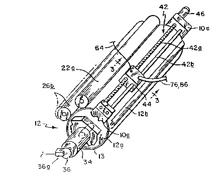
Also supported on frame lOa adjacent to cylinder 12 is a
writing head assembly shown generally at 42. This assembly
comprises a lead screw 42a whose opposite ends are rotatively
supported in the press frame lOa, which frame also supports the
opposite ends of a guide bar 42_ spaced parallel to lead screw
42a. Mounted for movement along the lead screw and guide bar
is a carriage 44. When the lead screw is rotated by a step
motor 46, carriage 44 is moved axially with respect to print
cylinder 12.
The cylinder drive motor 34 and step motor 46 are operated
in :iy~ ism by a controller 50 (FIG. 3), which also receives
signals from detector 36_, so that as the drum rotates, the
carriage 44 moves axially along the drum with the controller
"knowing" the instantaneous relative position of the carriage
and cylinder at any given moment. The control circuitry
required to accomplish this is already very well known in the
--14--
2053575
scanner and plotter art.
Refer now to FIG. 3 which depicts an illustrative
: ',,'ir ~ of carriage 44. It includes a block 52 having a
threaded opening 523 for threadedly receiving the lead screw
423 and a second parallel opening 52_ for slidably receiving
the guide rod 42k. A bore or recess 54 extends in from the
underside of block 52 for slidably receiving a discoid writing
head 57 made of a suitable rigid electrical insulating
material. An axial passage 57 extends through head 56 for
snugly receiving a wire electrode 58 whose diameter has been
exaggerated for clarity. The upper end 583 of the wire
electrode is received and anchored in a socket 62 mounted to
the top of head 56 and the lower end 58_ of the electrode 58 is
preferably pointed as shown in FIG. 3. Electrode 58 is made of
an electrically conductive metal, such as thoriated tungsten,
capable of withstanding very high t~, a~UL~S. An insulated
conductor 64 connects socket 62 to a t~rm;nAl 643 at the top of
block 52. If the carriage 44 has more than one electrode 58,
similar connections are made to those electrodes so that a
plurality of points on the plate 13 can be imaged
simultaneously by assembly 42.
Also formed in head 56 are a plurality of small air
p:~qS:A~C 66. These passages are distributed around electrode
58 and the upper ends of the passages are connected by way of
flexible tubes or hoses 68 to a corr~cp~ inq plurality of
vertical p~cqag~ 72. These passages extend from the inner
wall of block bore 54 to an air manifold 74 inside the block
which has an inlet passage 76 extending to the top of the
block. Passage 76 is connected by a pipe 78 to a source of
pL~s~uLized air. In the line from the air source is an
adjustable valve 82 and a flow restrictor 84. Also, a branch
line 783 leading from pipe 78 downstream from restrictor 84
connects to a pI S:~UL~ sensor 90 which produces an output for
controlling the setting of valve 82.
When the carriage 44 is positioned opposit~ plate 13 as
--15--
2053575
shown in FIG. 3 and air is supplied to its manifold 74, the air
issues from the lower ends of passages 66 with sufficient force
to support the head above the plate surface. The back ~LesS.u, e
in p~cce,goc 66 and manifold 74 varies directly with the spacing
of head 56 from the surface of plate 13 and this back pressure
is sensed by p~es~uLe sensor 90. The sensor controls valve 82
to adjust the air f low to head 56 so that the tip 58k of the
needle electrode 58 is maintained at a precisely controlled
very small spacing, e.g. 0.0001 inch, above the surface of
plate 13 as the carriage 44 scans along the surface of the
plate .
still referring to FIG. 3, the writing head 56, and
particularly the pulsing of its electrode 58, is controlled by
a pulse circuit 96. This circuit comprises a transformer 98
whose secondary winding 98a is connected at one end by way of a
variable resistor 102 to torminAl 64a which, as noted
previously, is connected electrically to electrode 58. The
opposite end of winding 98a is connected to electrical ground.
The transformer primary winding 98k is connected to a DC
voltage source 104 that supplies a voltage in the order of 1000
volts. The transformer primary circuit includes a large
capacitor 106 and a resistor 107 in series. The capacitor is
maintained at full voltage by the resistor 107. An electronic
switch 108 is connected in shunt with winding 98k and the
capacitor. This switch is controlled by switching signals
received from controller 50.
When an image is being written on plate 13, the press 10
is operated in a non-print or imaging mode with both the ink
and water rollers 22a and 26k being disengaged from cylinder
12. The imaging of plate 13 in press 10 is controlled by
controller 50 which, as noted previously, also controls the
rotation of cylinder 12 and the sc~nnin~ of the plate by
carriage assembly 42. The signals for imaging plate 13 are
applied to controller 50 by a conventional source of picture
signals such as a disk reader 114. The controller 50
2053575
synchronizes the image data from disk reader 114 with the
control signals that control rotation of cylinder 12 and
movement of carriage 44 so that when the electrode 58 is
positioned over uniformly spaced image points on the plate 13,
switch 108 is either closed or not closed dF~rc~n~l i ng upon
whether that particular point is to be written on or not
written on.
If that point is not to be written on, i . e . it corresponds
to a location in the ba~ ky vul~d of the original do~;l 1, the
electrode is not pulsed and proceeds to the next image point.
On the other hand, if that point in the plate does .w.Le~,l.d
to a location in the printed area of the original document,
switch 108 is closed. The closing of that switch discharges
capacitor 106 so that a precisely shaped, i.e. squarewave, high
voltage pulse, i . e. 1000 volts, of only about one microsecond
duration is applied to transformer 98. The transformer applies
a stepped up pulse of about 3000 volts to electrode 58 causing
a spark discharge S between the electrode tip 58b and plate 13.
That sparks and the accompanying corona field S' :,u~L~-ullding
the spark zone etches or transforms the surface of the plate at
the point thereon directly opposite the electrode tip 58_ to
render that point either receptive or non-receptive to ink,
~p"n~lin~ upon the type of surface on the plate.
The transformations that do occur with our different
lithographic plate constructions will be described in more
detail later. Suffice it to say at this point, that resistor
102 is adjusted for the different plate ~ 1ir l s to produce
a spark discharge that writes a clearly def ined image spot on
the plate surface which is in the order of 0 . 005 to 0 . 0001 inch
in diameter. That resistor 102 may be varied manually or
automatically via controller 50 to produce dots of variable
size. Dot size may also be varied by varying the voltage
and/or duration of the pulses that produce the spark
discharges. Means for doing this are quite well known in the
art. If the electrode has a pointed end 58_ as shown and the
2053575
--17--
gap between tip 58k and the plate is made very small, i.e.
0 . 001 inch, the spark discharge is focused so that image spots
as small as 0. 0001 inch or even less can be formed while
keeping voltage requirements to a minimum. The polarity of the
voltage applied to the electrode may be positive or negative
although preferably, the polarity is selected according to
whether ions need to be pulled from or repelled to the plate
surface to effect the desired surface transformations on the
various plates to be described.
As the electrode 58 is scanned across the plate surface,
it can be pulsed at a maximum rate of about 500, 000 pulses/sec.
However, a more typical rate is 25,000 pulses/sec. Thus, a
broad range of dot densities can be achieved, e.g. 2,000
dots/ inch to 50 dots/ inch . The dots can be printed side-by-
side or they may be made to overlap so that substantially 100%
of the surface area of the plate can be imaged. Thus, in
response to the ir in~ data, an image CoLL-r`L~ inlJ to the
original do ~ builds up on the plate surface constituted by
the points or spots on the plate surface that have been etched
or transformed by the spark discharge S, as compared with the
areas of the plate surface that have not been so affected by
the spark discharge.
In the case of axial scanning, then, after one revolution
of print cylinder 12, a complete image will have been applied
to plate 13. The press 10 can then be operated in its printing
mode by moving the ink roller 22a to its inking position shown
in solid lines in FIG. 1, and, in the case of wet printing, by
also shifting the water fountain roller 26k to its dotted line
position shown in FIG. 1. As the plate rotates, ink will
adhere only to the image points written onto the plate that
correspond to the printed portion of the original document.
That ink image will then be transferred in the usual way via
blanket cylinder 14 to the paper sheet P mounted to cylinder
16 .
Forming the image on the plate 13 while the plate is on
--18--
2053575
the cylinder 12 provides a number of advantages, the most
important of which is the signif icant decrease in the
preparation and set up time, particularly if the invention is
incorporated into a multi-color press. Such a press includes a
plurality of sections similar to press 10 described herein, one
for each color being printed. Whereas normally the print
cylinders in the different press sections after the first are
adjusted axially and in phase so that the different color
images printed by the lithographic plates in the various press
sections will appear in register on the printed copies, it is
apparent from the foregoing that, since the images are applied
to the plates 13 while they are mounted in the press sections,
such print registration can be ac~ 1 i ch~.rl electronically in
the present case.
More particularly, in a multicolor press, incorporating a
plurality of press sections similar to press 10, the controller
50 would adjust the timings of the picture signals controlling
the writing of the images at the second and subsequent printing
sections to write the image on the lithographic plate 13 in
each such station with an axial and/or angular offset that
- ~cates for any misregistration with respect to the image
on the first plate 13 in the press. In other words, instead of
achieving such registration by repositioning the print
cylinders or plates, the registration errors are accounted for
when writing the images on the plates. Thus once imaged, the
plates will automatically print in perfect register on paper
sheet P.
Refer now to FIGS. 4A to 4F which illustrate various
lithographic plate embodiments which are capable of being
imaged by the apparatus depicted in FIGS. 1 to 3. In FIG. 4A,
the plate 13 mounted to the print cylinder 12 comprises a steel
base or substrate layer 133 having a f lash coating 13_ of
copper metal which is, in turn, plated over by a thin layer 13c
of chrome metal . As described in detail in U. S . Patent
4,596,760, the plating process produces a surface topography
--19--
205~575
which is hydrophilic. Therefore, plate 13 is a preferred one
for use in a ~' -nin~-type offset press.
During a writing operation on plate 13 as described above,
voltage pulses are applied to electrode 58 so that spark
discharges S occur between the electrode tip 58_ and the
surface layer 13 of plate 13. Each spark discharge, coupled
with the accompanying corona f ield S ' surrounding the spark
zone, melts the surface of layer 13_ at the imaging point I on
that surface directly opposite tip 58k. Such melting suffices
to fill or close the capillaries at that point on the surface
so that water no longer tends to adhere to that surf ace area .
Accordingly, when plate 13 is imaged in this fashion, a
multiplicity of non-water-receptive spots or dots I are formed
on the otherwise hydrophilic plate surface, which spots or dots
represent the printed portion of the original document being
copied .
When press 10 is operated in its wet printing mode, i.e.
with rli ; nq assembly 24 in its position shown in phantom in
FIG. 1, the water from the -;n~ roll 26_ adheres only to
the surface areas of plate 13 that were not subjected to the
spark discharges from electrode 58 during the imaging
operation. On the other hand, the ink from the ink roll 22a
does adhere to those plate surface areas written on, but does
not adhere to the surface areas of the plate where the water or
wash solution is present. When printing, the ink adhering to
the plate, which forms a direct image of the original ~lo_ ~,
is transferred via the blanket cylinder 14 to the paper sheet P
on cylinder 16. While the polarity of the voltage applied to
electrode 58 during the imaging process described above can be
positive or negative, we have found that for imaging a plate
with a bare chrome surface such as the one in FIG. 4A, a
positive polarity is preferred because it enables better
control over the formation of the spots or dots on the surface
of the plate.
FIG. 4B illustrates another plate embodiment which is
2053575 -
--20--
written on directly and used in a 1 -n; n~-type press . This
plate, shown generally at 122 in FIG. 4B, has a substrate 124
made of a metal such as aluminum which has a structured oxide
surface layer 126. This surface layer may be produced by any
one of a number of known chemical treatments, in some cases
assisted by the use of f ine abrasives to roughen the plate
surface. The controlled oxidation of the plate surface is
commonly called anodizing while the surface structure of the
plate is referred to as grain or graining. As part of the
chemical treatment, modifiers such as silicates, phosphates,
etc. are used to stabilize the hydrophilic character of the
plate surface and to promote both adhesion and the stability of
the photosensitive layer(s) that are coated on the plates.
The aluminum oxide on the surface of the plate is not the
crystalline structure associated with CUL UlldUIII or a laser ruby
(both are aluminum oxide crystals), and shows considerable
interaction with water to form hydrates of the form Al2O3.H2O.
This interaction with contributions from silicate, phosphate,
etc . modif iers is the source of the hydrophilic nature of the
plate surface. Formation of hydrates is also a problem when
the process proceeds lln~h~ d. Eventually a solid hydrate
mass forms that effectively plugs and eliminates the structure
of the plate surface. Ability to effectively hold a thin film
of water required to produce nonimage areas is thus lost which
renders the plate useless. Most plates are supplied with
photosensitive layers in place that protect the plate surfaces
until the time the plates are exposed and developed. At this
point, the plates are either immediately used or stored for use
at a latter time. If the plates are stored, they are coated
with a water soluble polymer to protect hydrophilic surfaces.
This is the process usually referred to as gumming in the
trade. Plates that are supplied without photosensitive layers
are usually treated in a similar manner.
The loss of hydrophilic character during storage or
extended interruptions while the plate is being used is
--21--
2053575
generally referred to as oxidation in the trade. D~r~n~l;n~ on
the amount of structuring and chemical modifiers used, there is
a considerable variation in plate sensitivity to excessive
hydration .
When the plate 122 is subjected to the spark discharge
from electrode 58, the heat from the spark S and associated
corona S ' around the spark zone renders oleophilic or ink
receptive a precisely defined image point I opposite the
electrode tip 58_.
The behavior of the imaged aluminum plate suggests that
the image points I are the result of combined partial
processes. It is believed that dehydration, some formation of
fused aluminum oxide, and the melting and transport to the
surface of aluminum metal occur. The, ;n~cl effects of the
three processes, we suppose, reduce the hydrophilic character
of the plate surf ace at the image point . Aluminum is
chemically reactive with the result that the metal is always
found with a thin oxide coating regardless of how smooth or
bright the metal appears. This oxide coating does not exhibit
a hydrophilic character, which agrees with our observation that
an imaged aluminum-based plate can be stored in air more than
24 hours without the loss of an image. In water, aluminum can
react rapidly under both basic and acidic conditions including
several electrochemical reactions. The mildly acidic fountain
solutions used in presses are believed to have this effect on
the thin f ilms of aluminum exposed during imaging resulting in
their removal.
Because of the above-mentioned af f inity of the non-imaged
oxide surface areas of the plate for water, protection of the
just-imaged plate 122 requires that the plate surface be
shielded from contact with water or water-based materials.
This may be done by applying ink to the plate without the use
of a .li ;n~ or fountain solution, i.e. with water roll 26b
disengaged in FIG. 1. This results in the entire plate surface
being coated with a layer of ink. Dampening water is then
--22--
2053575
applied (i.e. the water roll 26_ is engaged) to the plate.
Those areas of the plate that were not imaged acquire a thin
film of water that dislodges the overlying ink allowing its
removal from the plate. The plate areas that were imaged do
not acquire a thin f ilm of water with the result that the ink
remains in place.
The images generated on a chrome plate with an oxide
surface coating show a similar sensitivity to water contact
preceding ink contact. However, after the ink application
step, the images on a chrome plate are more stable and the
plate can be run without additional steps to preserve the
image .
The ink I~ ~ ining on the image points I is quite fragile
and must be lef t to dry or set so that the ink becomes more
durable. Alternatively, a standard ink which cures or sets in
response to ultraviolet light may be used with plate 122. In
this event, a standard ultraviolet lamp 126 may be mounted
adjacent to print cylinder 12 as depicted in FIGS. 1 and 2 to
cure the ink. The lamp 126 should extend the full length of
cylinder 12 and be supported by frame members 10a close to the
surface of cylinder 12 or, more particularly, the lithographic
plate thereon.
We have found that imaging a plate such as plate 122
having an oxide surface coating is optimized if a negative
voltage is applied to the imaging electrode 58. This is
because the positive ions produced upon heating the plate at
each image point migrate well in the high intensity current
f low of the spark discharge and will move toward the negative
electrode .
FIG. 4C shows a plate embodiment 130 suitable for direct
imaging in a press without ~ nin~, Plate 130 comprises a
substrate 132 made of a conductive metal such as aluminum or
steel. The substrate carries a thin coating 134 of a highly
oleophobic material such as a fluoropolymer or silicone. One
suitable coating material is an addition-cured release coating
2053575 -
--23--
marketed by Dow Corning under its designation SYh-OFF 7044.
Plate 130 is written on or imaged by ~de_ -sing the surface of
coating 134 using spark discharges from electrode 58. The heat
from the spark and associated corona dr -Fe the silicone
coating into silicon dioxide, carbon dioxide, and water.
Hydrocarbon fragments in trace amounts are also possible
pGn~lin~ on the chemistry of the silicone polymers used.
Silicone resins do not have carbon in their b~ hnnPc which
means various polar ~u~;~ule6 such as C-OH are not formed.
Silanols, which are Si-OH structures are possible ~ue~u~eS~
but these are reactive which means they react to form other,
stable ~- u -ur èS
Such dec --ition coupled with surface rough~nin~ of
coating 134 due to the spark discharge renders that surface
oleorh; 1 i c~ at each image point I directly opposite the tip of
electrode 58. Preferably that coating is made quite thin, e.g.
0.0003 inch to m;n;m;7e the voltage required to break down the
material to render it ink receptive. Resultantly, when plate
130 is inked by roller 22a in press 10, ink adheres only to
those transr~ -1 image points I on the plate surface. Areas
of the plate not so imaged, c~.L~ -- Ain~ to the ba~ l~L-,u-,d
area of the original ~ to be printed, do not pick up ink
from roll 22a. The inked image on the plate is then
transferred by blanket cylinder 14 to the paper sheet P as in
any conventional of f set press .
FIG. 4D illustrates a lithographic plate 152 suitable for
indirect imaging and for wet printing. The plate 152 comprises
a substrate 154 made of a suitable conductive metal such as
aluminum or copper. Applied to the surface of substrate 154 is
a layer 156 of phenolic resin, parylene, diazo-resin or other
such material to which oil and rubber-based inks adhere
readily. Suitable positive working, subtractive plates of this
type are available from the Enco Division of American Hoechst
Co. under that company's designation P-800.
When the coating 156 is subjected to a spark discharge
2053575
-
--24--
from electrode 58, the image point I on the surface of layer
156 opposite the electrode tip 58k ~e_ ~ e~ under the heat
and becomes etched so that it readily accepts water. Actually,
if layer 156 is thick enough, substrate 154 may simply be a
separate flat electrode member A;qrosed opposite the electrode
58. Accordingly, when the plate 152 is coated with water and
ink by the rolls 26k and 223, respectively, of press 10, water
adheres to the image points I on plate 152 formed by the spark
discharges from electrode 58. Ink, on the other hand, shuns
those water-coated surface points on the plate CVLL~ ; ng to
the ba~ ~yL~ul,l or non-printed areas of the original ~
and adheres only to the non-imaged areas of plate 152.
Another offset plate suitable for indirect writing and for
use in a wet press is depicted in FIG. 4E. This plate,
indicated at 162 in that figure, consists simply of a metal
plate, for example, copper, zinc or stainless steel, having a
clean and polished surface 162a. Metal surfaces such as this
are normally oleorhil;f- or ink-receptive due to surface
tension. When the surface 162a is subjected to a spark
discharge from electrode 58, the spark and ancillary corona
field etch that surface creating small capillaries or fissures
in the surface at the image point I opposite the electrode tip
58k which tend to be receptive to or wick up water. Therefore,
during printing the image points I on plate 162, corrPqp~n~l;n~
to the bac}.~--,ul~d or non-printed areas of the original
dc L, receive water from roll 26k of press lO and shun ink
from the ink roll 22a. Thus ink adheres only to the areas of
plate 162 that were not subjected to spark discharges from
electrode 58 as described above and which correspond to the
printed portions of the original do., ~.
Refer now to FIG. 4F which illustrates still another plate
'-'; ~ 172 suitable for direct imaging and for use in an
offset press without ~ 1;n~J. We have found that this novel
plate 172 actually produces the best results of all of the
plates described herein in terms of the quality and useful life
-
--25--
2053575
of the image impressed on the plate.
Plate 172 comprises a base or substrate 174, a base coat
or layer 176 containing pigment or particles 177, a thin
conductive metal layer 178, an ink repellent silicone top or
surface layer 184, and, if n~ceCcAry~ a primer layer 186
between layers 178 and 184.
1. Substrate 174
The material of substrate 174 should have r - ' ~n i CA 1
, lack of extension (stretch) and heat resistance.
Polyester film meets all these requirements well and is readily
available . Dupont ' s Mylar and ICI ' s Nelinex are two
commercially available films. Other films that can be used for
.,~br~^te 174 are those based on polyimides (Dupont's Kapton)
and polycarbonates (GE's Lexan). A preferred thickness is
O. 005 inch, but thinner and thicker versions can be used
effectively.
There is no requirement for an optically clear film or a
smooth film surface (within reason). The use of pigmented
f ilms including f ilms pigmented to the point of opacity are
feasible for the substrate, providing mechanical properties are
not lost.
2. Base Coat 176
An important feature of this layer is that it is strongly
textured. In this case, "textured" means that the surface
topology has u.lS peaks and valleys. When this surface is
coated with the thin metal layer 178, the projecting peaks
create a surface that can be described as containing numerous
tiny electrode tips (point source electrodes) to which the
spark from the imaging electrode 58 can jump. This texture is
conveniently created by the f iller particles 177 included in
the base coat, as will be described in detail hereinafter under
the section entitled Filler Particles 177. Other requirements
of base coat 176 include:
--26--
20535 75
a) adhesion to the substrate 174;
b) metAlli~hle using typical processes such as vapor
deposition or sputtering and providing a surface to
which the metal(s) will adhere strongly;
c) resistance to the ~ ~nts of offset printing inks
and to the cl~AninrJ materials used with these inks;
d) heat resistance; and
e) fl~Yihjlity equivalent to the substrate.
The chemistry of the base coat that can be used is wide
ranging. Application can be from solvents or from water.
Alternatively, 100% solids coatings such as characterize
conventional UV and EB curable coating can be used. A number
of curing methods (~-h~micAI reactions that create crosslin~ing
of coating ~ ) can be used to establish the performance
properties desired of the coatings. Some of these are:
a) .~- Typical ~h' - _ 1. reactions are those as an
aminoplast resin with hydroxyl sites of the primary
coating resin. These reactions are greatly
accelerated by creation of an acid environment and the
use of heat.
b) Isocvanate Based One typical approach are two part
urethanes in which an isocynate ~ - ~ reacts with
hydroxyl sites on one or more "backbone" resins often
referred to as the "polyol" ~. Typical
polyols include polyethers, polyesters, an acrylics
having two or more hydroxyl functional sites.
T ~dl ~ modifying resins include hydroxyl functional
vinyl resins and cellulose ester resins. The
isocyanate component will have two or more isocyanate
groups and is either monomeric or oligomeric. The
reactions will proceed at ambient temperatures, but
can be accelerated using heat and selected catalysts
which include tin compounds and tertiary amines. The
normal technique is to mix the isocynate functional
c -nt(s) with the polyol component(s) just prior
2053575
--27--
to use. The reactions begin, but are slow enough at
ambient temperatures to allow a "potlife" during which
the coating can be applied.
In another approach, the isocyanate is used in a
"blocked" form in which the isocyanate ~ t has
been reacted with another . ~ t such as a phenol
or a ketoxime to produce an inactive, metastable
~ _ '. This __ ' is designed for flr , ition
at elevated t~ c.Lu.es to liberate the active
isocyanate ~ -nt which then reacts to cure the
coating, the reaction being accelerated by
incorporation of appropriate catalysts in the coating
f ormulation .
c) Aziridines The typical use is the crosslinking of
waterborne coatings based on carboxyl functional
resins. The carboxyl groups are incorporated into the
resins to provide sites that form salts with water
soluble amines, a reaction integral to the
solubilizing or dispersing of the resin in water. The
reaction ~Luceeds at ambient temperatures after the
water and solubilizing amine(s) have been ev~pc~c.ted
- upon deposition of the coating. The aziridines are
added to the coating at the time of use and have a
potlife yuveL~Ied by their rate of hydrolysis in water
to produce inert by-products.
d) EPoxY Reactions The elevated-temperatures cure of
boron trif luoride complex catalyzed resins can be
used, particularly for resins based on cycloaliphatic
epoxy functional groups. Another reaction is based on
W exposure generated cationic catalysts for the
reaction. Union Carbide ' s Cyracure system is a
commercially available version.
e) Radiation Cures are usually free radical
polymerizations of mixtures of monomeric and
oligomeric acrylates and methacrylates. Free radicals
2053575
--28--
to initiate the reaction are created by exposure of
the coating to an electron beam or by a
photoinitiation system incv.yvl~lted into a coating to
be cured by W exposure.
The choice of chemistry to be used will depend on the
type of coating equipment to be used and environmental
concerns rather than a limitation by required
performance properties. A crossl ;nl~ing reaction is
also not an absolute requirement. For example, there
are resins soluble in a limited range of solvents not
including those typical of offset inks and their
cleaners that can be used.
3. Filler Particles 177
The f iller particles 177 used to create the important
surface structure are chosen based on the following
cons iderations:
a) the ability of a particle 177 of a given size to
contribute to the surface structure of the base coat
176 . This is dPrpn~l~nt on the th; ~ npeq of the
coating to be deposited. This is illustrated for a 5
micron thick t . 0002 inch) coat 176 pigmented with
particles 177 of spherical g~ -y that remain well
dispersed throughout deposition and curing of the
coat. Particles with diameters of 5 microns and less
would not be expected to contribute greatly to the
surface ~Lu.:~ule because they could be contained
within the thickness of the coating. Larger
particles, e.g. 10 microns in diameter, would make
significant contributions because they could project 5
microns above the base coat 176 surface, creating high
points that are twice the average thickness of that
coat .
b) the ge L.y of the particles 177 is important.
Equidimensional particles such as the spherical
205~575
--29--
particles described above and depicted in FIG. 4F will
contribute the same degree regardless of particle
orientation within the base coat and are therefore
preferred. Particles with one dimension much greater
than the others, acicular types being one example, are
not usually desirable. These particles will tend to
orient themselves with their long dimensions parallel
to the surface of the coating, creating low rounded
ridges rather than the desirable distinct peaks.
Particles that are platelets are also undesirable.
These particles tend to orient themselves with their
broad dimensions (faces) parallel to the coating
surface, thereby creating low, broad, rounded mounds
rather than desirable, distinct peaks.
c) the total particle content or density within the
coating is a function of the image density to be
encountered. For example, if the plate is to be
imaged at 400 dots per centimeter or 160,000 dots per
square centimeter, it would be desirable to have at
least that many peaks (particles) present and
positioned so that one occurs at each of the possible
positions at which a dot may be created. For a
coating 5 microns thick, with peaks produced by
individual particles 177, this would correspond to a
density of 3 . 2 x 1o8 particles/cubic centimeter (in
the dried, cured base coat 176).
Particle sizes, geometries, and densities are readily
available data for most filler particle candidates, but there
are two important complications. Particle sizes are averages
or mean valves that describe the distribution of sizes that are
characteristic of a given powder or pigment as supplied. This
means that both larger and smaller sizes than the average or
mean are present and are signif icant contributors to particle
size considerations. Also, there is always some degree of
- 2053575
--30--
particle association present when particles are dispersed into
a fluid medium, which usually increases during the application
and curing of a coating. Resultantly, peaks are produced by
groups of particles, as well as by individual particles.
Preferred filler particles 177 include the following:
a) amorphous silieas (via various commereial processes)
b) mi~ y~-alline silieas
e) synthetic metal oxides (single and in multi-_ - L
mixtures)
d) metal powders (single metals, mixtures and alloys)
e) graphite (synthetic and natural)
f ) carbon black (via various eommercial processes)
Preferred particle sizes for the filler partieles to be
used is highly ~l~ron~ nt on the thickness of the layer 176 to
be deposited. For a 5 micron thick layer (preferred
application), the preferred sizes fall into one of the
following two ranges:
a) 10 +/- 5 microns for particles 177 that act
~L~F' inAntly as individuals to create surface
:, L. u~; Lu~ .a, and
b) 4 +/- 2 microns for particles that act as groups
(agglomerates) to create surface structure.
For both particle ranges, it should be understood that
larger and smaller sizes will be present as part of a size
distribution range, i.e. the values given are for the average
or mean particle size.
The method of coating base layer 176 with the particles
177 dispersed therein onto the substrate 174 may be by any of
the currently available commercial coating processes.
A preferred application of the base coat is as a layer 5
+/- 2 microns thick. In practice, it is expected that base
coats could range from as little as 2 microns to as much as 10
2 0 5 3 5 75
--31--
microns in thickness. Layers thicker than lO microns are
possible, and may be required to produce plates of high
durability, but there would be considerable difficulty in
texturing these thick coatings via the use of filler pigments.
Also, in some cases, the base coat 176 may not be required
if the substrate 174 has the proper, and in a sense equivalent,
properties. More particularly, the use for substrate 174 of
films with surface textures t:~-Lu-;LuL~s) created by mechanical
means such as embossing rolls or by the use of f iller pigments
may have an important advantage in some applications provided
they meet two conditions:
a) the films are metalizable with the deposited metal
forming layer 178 having adequate adhesion; and
b) their film surface texture produces the important
feature of the base coat described in detail above.
4. Thin Metal LaYer 178
This layer 178 is; ~dllL to formation of an image and
must be uniformly present if uniform imaging of the plate is to
occur . The image carrying ( i . e . ink receptive) areas of the
plate 172 are created when the spark discharge volatizes a
portion of the thin metal layer 178. The size of the feature
formed by a spark discharge from electrode tip 58b of a given
energy is a function of the amount of metal that is volatized.
This is, in turn, a function of the amount of metal present and
the energy required to volatize the metal used. An; .~ ~d~
modif ier is the energy available from oxidation of the
volatized metal (i.e. that can contribute to the volatizing
process), an important partial process present when most metals
are vaporized into a routine or ambient atmosphere.
The metal preferred for layer 178 is aluminum, which can
be applied by the process of vacuum metallization (most
commonly used) or sputtering to create a uniform layer 300 +/-
100 Any;,~L, ~ thick. Other suitable metals include chrome,
copper and zinc. In general, any metal or metal mixture,
2053575 -
--3~:--
including alloys, that can be deposited on base coat 176 can be
made to work, a consideration since the sputtering process can
then deposit mixtures, alloys, refractories, etc. Also, the
thickness of the deposit is a variable that can be ~rAn~l~d
outside the indicated range. That is, it is possible to image
a plate through a 1000 Angstrom layer of metal, and to image
layers less than 100 AnyDL. - thick. The use of thicker
layers reduces the size of the image formed, which is desirable
when resolution is to be i uve:d by using smaller size images,
points or dots.
5. Primer 186 (when reauired~
The primer layer 186 anchors the ink repellent silicone
coating 184 to the thin metal layer 178. Effective primers
include the following:
a) silanes (monomers and polymeric forms)
b. titanates
c) polyvinyl alcohols
d) polyimides and polyamide-imides
Silanes and titanates are deposited from dilute solutions,
typically 1-3% solids, while polyvinyl alcohols, polyimides,
and polyamides-imides are deposited as thin f ilms, typically 3
+/- 1 microns. The techniques for the use of these materials
is well known in the art.
6. Ink RePellent silicone Surface La~er 184
As pointed out in the ba~kyL uul)d section of the
application, the use of a coating such as this is not a new
concept in offset printing plates. ~owever, many of the
variations that have been proposed previously involve a
photosensitizing -^hAn; C.m, The two general approaches have
been to incorporate the photoresponse into a silicone coating
formulation, or to coat silicone over a photosensitive layer.
When the latter is done, photoexposure either results in f irm
anchorage of the silicone coating to the photosensitive layer
~33~ 2053575
so that it will remain after the developing process removes the
unexposed silicone coating to create image areas (a positive
working, subtractive plate) or the ~ JOb~UL~ destroys anchorage
of the silicone coating to the photosensitive layer so that it
is removed by "developing" to create image areas leaving the
...,_,.I riced silicone coating in place (a negative working,
subtractive plate). Other approaches to the use of silicone
coatings can be described as modif ications of xeL ~yL ~phic
pL ~cesses that result in an image-carrying material being
implanted on a silicone coating followed by curing to establish
durable adhesion of the particles.
Plates marketed by IBM Corp. under the name Electroneg use
a silicone coating as a protective surface layer. This coating
is not formulated to release ink, but rather is removable to
allow the plates to be used with rl ; ng water applied.
The silicone coating here is preferably a mixture of two
or more ~ --ts, one of which will usually be a linear
silicone polymer terminated at both ends with functional
(rhPmi~-_l ly reactive) groups. Alternatively, in place of a
linear difunctional silicone, a copolymer incorporating
functionality into the polymer chain, or branched :~LLU-:LULeS
terminating with functional groups may be used. It is also
possible to combine linear difunctional polymers with
copolymers and/or branch polymers. The second - ent will
be a multifunctional monomeric or polymeric nPj-t reactive
with the first ~ C:--L. Additional s LS and types of
functional groups present will be discussed for the coating
chemistries that follow.
a) C~-n~lPncation Cure Coatinqs are usually based on
silanol (-si-o~) terminated polydimethylsiloxane polymers (most
commonly linear). The silanol group will ~-ondPn~P with a
number of multifunctional silanes. Some of the reactions are:
2053575
--34--
Functional Reaction BYProduct
Group
O~ o
Acetoxy -Si-oH + RCo-si- -si-o-si- + HOCR
Alkoxy --Si--oH + Ro--Si-- --si--o--si-- + HOR
Oxime -Si-oH + R1R2C=No-Si- -Si-O-Si- + HON=CRlR2
Catalysts such as tin salts or titanates can be used to
accelerate the reaction. Use of low molecular weight groups
such as CH3- and CH3CH2- for R1 and R2 also help the reaction
rate yielding volatile byproducts easily removed from the
coating. The silanes can be difunctional, but trifunctional
and tetrafl~n~tit~n~l types are preferred.
C~ dtion cure coatings can also be based on a moisture
cure approach. The functional groups of the type indicated
above and others are subject to hydrolysis by water to liberate
a silanol functional silane which can then condense with the
silanol groups of the base polymer. A particularly favored
approach is to use acetoxy functional silanes, because the
L~ lu~L, acetic acid, contributes to an acidic environment
favorable for the cnn~l~n~ation reaction. A catalyst can be
added to promote the cnn~ n~ation when neutral byproducts are
produced by hydrolysis of the silane.
Silanol groups will also react with polymethyl
hydrosiloxanes and polymethylhydrosiloxane copolymers when
catalyzed with a number of metal salt catalysts such as
dibutyltindiacetate. The general reaction is:
-Si-oH + --H-SI- --(catalyst)--> Si-O-Si- + H2
This is a preferred reaction because of the requirement
for a catalyst. The silanol terminated polydimethylsiloxane
polymer is blended with a polydimethylsiloxane second component
2053575 -
--35--
to produce a coating that can be stored and which is catalyzed
just prior to use. Catalyzed, the coating has a potlife of
several hours at ambient t~ ~Lu,~s, but cures rapidly at
elevated t~ ~LUL~S such as 300F. Silanes, preferably
acyloxy functional, with an appropriate second functional group
(carboxy rh~ Led, and glycidoxy are examples) can be added
to increase coating adhesion. A working example follows.
b) Addition Cure Coatings are based on the
hydrosilylation reaction; the addition of Si-H to a double bond
catalyzed by a platinum group metal complex. The general
reaction is:
-Si-H + CH2=CH-Si- -- (catalyst) --> -Si-CH2CH2-Si-
Coatings are usually formulated as a two part systemc -- ~ of a vinyl functional base polymer (or polymer blend)
to which a catalyst such as a chloroplantinic acid complex has
been added along with a reaction modifier(s) when c-~L.,~Liate
(cyclic vinyl-methylsiloxanes are typical modifiers), and a
second part that is usually a polymethylhydrosiloxane polymer
or copolymer. The two parts are _ ~;nD-l just prior to use to
yield a coating with a potlife of several hours at ambient
temp~L~Lu,.as that will cure rapidly at elevated temperatures
(300~F, for example). Typical base polymers are linear
vinyldimethyl terminated polydimethylsiloxanes and
dir Llly~iloxane-vinylmethylsiloxane copolymers. A working
example follows.
c) Radiation Cure Coatinqs can be divided into two
approaches. For U.V. curable coatings, a cationic --- -ni rm is
preferred because the cure is not inhibited by oxygen and can
be accelerated by post U.V. exposure application of heat.
Silicone polymers for this approach utilize cycloaliphatic
epoxy functional groups. For electron beam curable coatings, a
free radical cure DF hAn; Fm is used, but requires a high level
of inerting to achieve an adequate cure. Silicone polym~ers for
2053575
--36--
this approach utilize acrylate functional groups, and can be
crosslinked effectively by multifunctional acrylate ~
Preferred base polymers for the surface coatings 184
discussed are based on the coating approach to be used. When a
solvent based coating is formulated, preferred polymers are
medium molecular weight, difunctional polydimethylsiloxanes, or
difunctional polydimethyl-siloxane copolymers with
dimethylsiloxane . --in~ 80% or more of the total polymer.
Preferred molecular weights range from 70,000 to 150,000. When
a 100% solids coating is to be applied, lower molecular weights
are desirable, ranging from 10,000 to 30,000. Higher molecular
weight polymers can be added to improve coating properties, but
will comprise less than 20% of the total coating. When
addition cure or ~-- AC- ~ ion cure coatings are to be
formulated, preferred second ~ L~ to react with silanol
or vinyl fllnrt;onAl groups are polymethylhydrosiloxane or a
polymethylhydrosiloxane copolymer with dimethylsiloxane.
Preferably, selected filler pigments 188 are incorporated
into the surface layer 184 to support the imaging process as
shown in FIG. 4F. The useful pigment materials are diverse,
including:
a) Al ; powders
b) molybdenum disulf ide powders
c) synthetic metal oxides
d) silicon carbide powders
e) graphite
f ) carbon black
Preferred particle sizes for these materials are small,
having average or mean particle sizes considerably less than
the thickness of the applied coating (as dried and cured). For
example, when an 8 micron thick coating 184 is to be applied,
preferred sizes are less than 5 microns and are preferably, 3
microns or less. For thinner coatings, preferred particle
sizes are decreased accordingly. Particle 188 geometries are
not an important ~on~ideration. It is desirable to have all
2053575 -
--i7--
the particles present enclosed by the coating 184 because
particle surfaces projecting at the coating surface have the
potential to decrease the ink release properties of the
coating. Total pigment content should be 20% or less of the
dried, cured coating 184 and preferably, less than 10% of the
coating. An aluminum powder supplied by C~ncol i~l~ted
A~L..J~-~u~ics as 3 micron sized particles has been found to be
satisfactory. Contributions to the imaging process are
believed to be conductive ions that support the spark (arc)
from electrode 58 during its brief existence, and considerable
energy release from the highly exothermic oxidation that is
also believed to occur, the liberated energy contributing to
de- -~ition and volatilization of material in the region of
the image forming on the plate.
The ink repellent silicone surface coating 184 may be
applied by any of the available coating processes. One
consideration not u.._ to coating processes in general, is
to produce a highly uniform, smooth, level coating. When this
is achieved, the peaks that are part of the structure of the
base coat will project well into the silicone layer. The tips
of these peaks will be thin points in the silicone layer, as
shown at 184 ' in FIG. 4F, which means the insulating effect of
the silicone will be lowest at these points contributing to a
spark jumping to these points. These projections of the base
coat 176 peaks due to particles 177 therein are depicted at P
in FIG. 4F.
Workinq ExamPles of Ink F~ePellent Silicone Coatinqs
1. Commercial Condensation cure coating supplied by Dow
Corning:
C r-nt TvPe Parts
Syl--Off 294 sase coating 40
VM&P Naptha Solvent 110
2053575
--38--
Methy1 Ethyl Ketone Solvent 50
Aluminum Powder Filler Pigment
Blend/Disperse Powder/Then Add:
syl-off 297 Acetoxy Functional Silane 1. 6
81end/Then Add:
XY-176 Catalyst Dibutyltin~ cetate
Blend/Then Use:
Apply with a ~Y10 Wire Wound Rod
Cure at 300F for 1 minute
2. Commercial addition cure coating supplied by Dow Corning:
C~ -nt ~ Parts
Syl-Off 7600 Base Coating 100
VM-P Naptha Solvent 8 0
Methyl Ethyl Ketone Solvent 40
Alimiml"~ Powder Filler Pigment 7.5
Blend/DisPerse Powder/Then Add:
Syl-Of f 7 6 01 Cross 1 inker 4 . 8
Blend/Then Use:
Apply with a ,~4 Wire Wound Rod
Cure at 300F for 1 minute
This coating can also be applied as a 100% solids coating (same
formula without solvents) via offset gravure and cured using
the same conditions.
3. Lab coating formulations illustrating condensation cure and
addition cure coatings are given in the following Table 1.
Identity of indicated -, ~s are given in the following
Table 2. All can be applied by coating with wire wound rods
and cured in a convection oven set at 300F using a 1 minute
dwell time. Coating 4 can be applied as a 100% solids coating
and cured under the same conditions.
-39- 2053575 -
, I,,, ,,,, o ~
~ ~ I I o I ,~ In O O ~
I I I ~ , I I o o m
o
.
,, o,,, ~ ~
m . I, I , I o ul u~
o
o
.
- - I O I I I I ~i I I N t~l I C~ Ul t`~
O O I I I I I I .0 I N 1~ 1 r O
O I I I I I ~ I I ~ ~ I 0 o
C,
-
V r
o
r~ ~ o ~ o . u~
~ ~ N '~ '~ .t ~ N
W W W U~ W W W W ~1 C.)
--40--
_ 2053575
.
., .,, ~ ~ ~ , .
. . , , ,~
~ O
0 0 Oo 0 0 ~o I o
r O ~ 1~1 ~0 ~ O N
_~ 5
_ _ _
5 5 r ' I
C ~ ~
5l ~ r 5
Ul
_ I _
_ ~ ~ r ~
~ cl U
~ 5
r ~
.~ U~ -
_ _ _ o ~ ~
_ _ . . ~ . O,--, ~ _
o ~, o U~
I ~ I I I I I 1 ~ 0
2053575
--41--
When plate 172 is subjected to a writing operation as
described above, electrode 58 is pulsed, preferably negatively,
at each image point I on the surface of the plate. Each such
pulse creates a spark discharge between the electrode tip 58k
and the plate, and more particularly across the small gap d
between tip 58k and the r ' 11 il'. underlayer 178 at the location
of a particle 177 in the base coat 176, where the repellent
outer coat 184 is thinnest. This localizing of the discharge
allows close control over the shape of each dot and also over
dot pl ~ l to r~ e image accuracy. The spark discharge
etches or erodes away the ink repellent outer layer 184
(including its primer layer 186, if present) and the metallic
underlayer 178 at the point I directly opposite the electrode
tip 58k thereby creating a well I ' at that image point which
exposes the underlying oleoFhi l ;c surface of base coat or layer
176. The pulses to electrode 58 should be very short, e.g. 0.5
microseconAc to avoid arc "fingering" along layer 178 and
c~ne~ nt melting of that layer around point I. The total
thickness of layers 178, 182 and 184, i . e . the depth of well
I ', should not be so large relative to the width of the image
point I that the well I' will not accept conventional offset
inks and allow those inks to offset to the blanket cylinder 14
when printing.
Plate 172 is used in press lo with the press being
operated in its dry printing mode. The ink from ink roller 22a
will adhere to the plate only to the image points I thereby
creating an inked image on the plate that is transferred via
blanket roller 14 to the paper sheet P carried on cylinder 16.
Instead of providing a separate metallic underlayer 178 in
the plate as in FIG. 4F, it is also feasible to use a
conductive plastic film for the conductive layer. A suitable
conductive material for layer 184 should have a volume
resistivity of 100 ohm centimeters or less, Dupont's Kapton
film being one example.
To facilitate spark discharge to the plate, the base coat
2053575
--42--
176 may also be made conductive by inclusion of a conductive
pigment such as one of the preferred base coat pigments
identif ied above .
Also, instead of producing peaks P by particles 177 in the
base coat, the substrate 174 may be a film with a textured
surface that forms those peaks. Polycarbonate films with such
surfaces are available from General Electric Co.
Another li-llO~LCl~lliC plate suitable for direct imaging in
a press without ~' ;n~ is illustrated in FIG. 4G. Reference
numeral 230 denotes generally a plate comprising a heat-
resistant, ink-receptive substrate 232, a thin conductive metal
layer 234, and an ink-repellent surface layer 236 containing
image-support material 238, as described below. In operation,
plate 230 is written on or imaged by pulsing electrode 58 at
each image point I on the surface of the plate. Each such
pulse creates a spark discharge between the electrode tip 58_
and the point on the plate directly opposite, destroying the
portions of both the ink-repellent outer layer 236 and thin-
metal layer 234 that lie in the path of the spark, thereby
exposing ink-receptive substrate 232. Because thin-metal layer
234 is grounded and ink-receptive substrate 232 resists the
effects of heat, only the thin-metal layer 234 and ink-
repellent surface 236 are volatized by the spark discharge.
Ink-receptive substrate 232 is preferably a plastic film.
Suitable materials include polyester f ilms such as those
marketed under the tra~l~n~r - MYLAR (E.I. duPont de Nemours)
or MELINEX (ICI). Thin-metal layer 234 is preferably aluminum
deposited as a layer from 200 to 500 aD~a~. - thick. Other
materials suitable for thin metal layer 234 and ink-receptive
substrate 232 are described above in connection with
co~Le:,l,v~lding layers 178 and 174, respectively, in FIG. 4F.
Image-support material 238 is most advantageously
dispersed in silicone, of the type described in connection with
surface layer 184 in FIG. 4F. If n~ cs~ry, a primer coat (not
depicted in Fig. 4G) may be added between thin-metal layer 234
2053575
-
--43--
and surface layer 184 to provide anchoring between these
layers .
The function of image _~.~pu. ~ material 238 is to promote
straight-line travel of the spark as it emerges from electrode
tip 58_. Producing this behavior reliably has proven one of
the most difficult aspects of spark-discharge plate design,
because even slight lateral migration of the spark path
produces unacceptably distorted images.
The path followed by an emitted spark is not actually
random, but rather is determin~d by the direction of the
electric f ield existing between the imaging electrode and the
surface of the plate. This field is created when an imaging
pulse is f irst directed to the electrode . A spark forms only
after the medium between the electrode and the plate surface
has ionized due to the energy of the field, a process which
requires a measurable amount of time. Ionization of the medium
provides the conductive pathway along which the spark travels.
Once the spark is formed, it remains in existence for the
r. inin~ duration of the image pulse. If the plate surface is
not conductive, it, too, must be broken down by the electric
field, which may result in the passage of additional time prior
to spark formation. During the cumulative duration of these
delays, the electric f ield may become distorted due to the
changes occurring in the medium and/or on the plate surface,
resulting in an irregular spark path.
Although one might assume that particles ~ ~sed of a
highly conductive material would serve as a useful spark-
guiding filler material, we have found that this is not the
case; we have also found that the distribution of such
particles does not materially deter the spark from following an
apparently random path. In a random dispersion of particles,
there can be no guarantee that the particle directly opposite
the electrode tip will also be closest ( in terms of linear
distance) to the electrode tip; nor is distance always
determinative, since a dense area of particles can provide a
-44- 2053575
~L~v~ r attraction for the spark than a single particle lying
closer to the electrode (so long as the additional distance to
the dense area is not too great). A non-random distribution of
particles can result in regions of pure silicone that contain
no particles; if such a region occurs directly opposite the
electrode when a pulse is delivered, the spark will probably
deviate from a straight-line path toward a more conductive
silicone region.
We have experimented with such conductive materials as
graphite, carbon black, and metal powders; these can be used to
pigment q; 1 ;r~nP coatings to render such coatings conductive,
and are often cited in the prior art. Carbon blacks and
graphites are available as particles which are sufficiently
small to avoid undesirable creation of a surface texture, and
can be used to produce coatings that remain stable as
dispersions. We have found, however, that when a quantity of
one or more of these materials sufficient to affect the imaging
process is introduced into an oleophobic coating, reduction of
oleophobic character can occur, with the consequence that
unwanted ink will adhere to the non-image portions of the plate
during printing. Carbon blacks and graphites can also react
adversely with some of the catalysts normally used for
thPrr- 1 1 y cured silicone coatings .
Conductive metal powders typically are not available in
usefully small particle sizes, and tend to be excessively dense
and lacking in surface area to permit formation of stable
dispersions. Although metal powders are successfully used in a
large number of paints and coatings characterized by high
viscosity and solids content, such materials yield compositions
that are far too thick for use as imageable plate coatings.
Yet even if these undesirable characteristics of
conductive particles could be overcome, our experiments suggest
that such particles would contribute to imaging only in a
limited fashion. Instead, we have found that certain types of
materials, including many semiconductors, support accurate
~45~ 2053575
imaging by promoting straight-line spark discharge. These
materials frequently have 6tructures that allow polarization by
a strong electric f ield, and also contain conduction bands of
suf f iciently low energy to be rendered accessible by
polarization; alternatively, a suitable material may respond to
a strong electric f ield by populating available conduction
bands to a much greater extent than would be obtained in the
absence of the f ield. Such materials undergo a pronnllnA~d
increase in conductivity, relative to that of yLuul.~ ~tate or
low-voltage conditions, when exposed to an electric f ield of at
least 1,000 volts. We herein refer to such ~ _ullds as
"conditionally conductive".
One group of useful . '- includes metal oxides whose
crystals contain two or more metal ions of different oxidation
states bound to the appropriate number of oxide ions to
pL~S~ electrical neutrality. The metal ion species may
derive from the same or different metals. A second type of
' comprises metal oxide ~_ '-, of the same or
different oxidation states, that polarize significantly in the
presence of a strong electric f ield. A third, related category
of ~_ _ ' includes a variety of "doped" metal-oxide
materials, in which relatively small, non-stoichiometric
amounts of a second metal are present. In a fourth type of
_u--d, a metal atom or ion is bound to a relatively
ele~;~L~.Ieycltive species such as sulfur, nitrogen, arsenic,
rho~.h~., Us, antimony, bismuth, carbon, or silicon. Another
type comprises high-Tc (i.e. 70-100 ~K) superconductor
materials and related precursors . We have also identif ied a
number of conditionally conductive compounds that do not fall
within any of the foregoing categories.
Without being bound to any particular theory or T--AhAn; F~,
we believe that the observed tendency of useful image-support
compounds to promote straight-line spark discharge is due
primarily to crystal and electronic structure. Low-energy
electron migration pathways within the crystal, induced or
-46- ~053575
Dnh in~ D~1 by the strong electric field centered at the electrode
tip during pulsing, channel electrons into the underlying thin-
metal layer. Due to geometric configuration, the point on the
plate surface immediately opposite the electrode tip will be
exposed to the electric field most directly. Conditionally
conductive semiconductor particles in the path of this f ield
will tend to become more conductive as a result of polarization
or conduction-band population, ~, a~ ening the field gradient
between the electrode tip and the plate surface. This
phr- occurs prior to arcing of the spark. With the
altered crystals providing a current-f low conduit of lower
resistance than that of the unaffected crystals and ~u~uul~ding
oleophobic medium, the spark is en. ..u~ d to follow the path
of least resistance through these particles to the plate, and
thereby follow a straight-line path. Imaging accuracy might be
further Dnh~n~D~l by lo~ ~l i 70 ~ heating of the altered crystals
as the spark begins to form, which may further increase their
conductivities .
This effect contrasts markedly to that generated by
particles whose conductivities are not affected by an electric
field. Such particles do not offer a preferred path for
conduction, and straight-line spark travel will be promoted
only at those points where the most favorable distribution of
particles occurs opposite the electrode tip. Using the
conditionally conductive particles of the present invention, we
have found that a random distribution of particles assures the
greatest degree of gradient strengthening, because distortions
due to particle position are statistically minimized.
For a ,- .u-ld to exhibit the necessary response to a
strong electric field, its crystalline form apparently must
possess a ~ Ul ~ and electronic conf iguration that results
either in (i) susceptibility to polarization by a strong
electric field, resulting in increased accessibility of
available conduction bands through lowering of the energetic
levels of such bands, or (ii) increased population of existing
2053575
--47--
conduction bands without energetic modif ication . It should be
noted that polarizability, in and of itself, in no way
guarantees that a material will be conditionally conductive,
since polarization can reduce the AC-~ce;hility of a conduction
band as well as improve it. As we will show, conduction bands
that are entirely ;nAcc~e~s;hle in the absence of a strong field
-- rendering the ~_ ' a relatively poor conductor -- can
nonetheless serve to produce a l~ eryy pathway for electron
migration, and produce good spark-guiding properties.
Polarizability is a characteristic determined by crystal
structure, and the electron affinities of the various atoms and
ions therein. Atoms and ions in a polarizable crystal shift
position in response to an electric field, allowing the crystal
to take on the charge distribution of the f ield and thereby
augment the overall f ield gradient. In the context of the
present invention, altering the ~y ~ y of the crystal results
in ~nhAn~-ed conductivity and/or degradation of barriers to
conductivity .
The field-induced availability of conduction bands within
the crystal can arise from any of a number of physical
attributes:
a. The crystal lattice allows a physical feature,
such as a plane or chain of ions, to extend across a crystal
grain, thereby providing a low-energy pathway for electron
migration .
b. The crystal lattice contains metal and non-metal
atoms or ions placed such that metal d orbital and non-metal p
(or np) orbital overlap occurs.
c. The potential energy of the crystal lattice is
not appreciably elevated by delocalization of one or more d-
orbital electrons from the metal atom or ion into a conduction
band .
d. Antiferromagnetic "pinning" of outer-shell
electrons, which under ordinary conditions completely precludes
-48- 2053575
virtually all conductivity, is overcome by field-induced
polarization .
1. Types of C . _ '~
Sinale-Metal Oxides
The following oxides of a single metal, in which the metal
ion is present in one or more oxidation states, promote imaging
(where formulae are enclosed in parenthesis, the first metal is
in the +2 state , the second in the +3 state):
Fe3o4 ( FeFe24 )
Gamma Fe203
Co304 ( CoC020g )
Mn3o4 (MnMn24)
Pb304 ( Pb2PbO4, +2 / +4 )
PbO2
CrO2
ZnO
MnO2
Mo02
NbO2
SnO
SnO2
Cu20
CuO
Tio
Ti23
V23
VO2
WO2
wo3
In203
~49~ 2053575
The +2/+3 oxidation state ~ ~c, Fe304 and Co304 are
probably conductive due to a rapid valence oscillation between
the metal sites in the crystal lattice, which results in the
transfer of positive charge from cation to cation; this effect
iS anhAn--ad in the presence of an electric field, resulting in
the formation of a low-energy pathway for electron migration.
See, e.g., W. Xingery, H. Bowen and D. Uhlmann, Introduction to
Ceramics (1976) at 899-902.
of the foregoing ~ '-, Fe3O4 and Co304 exert the
o~ aL spark-guiding effect. Both exhibit ~y LiC,
i ~ ic crystal structures. Although Mn3O4 might be
PYpected to exhibit similar valence oscillation due to
comparable ele~ ~L~ ~ive characteristics, we have found that
this . _ ' does not function as well as Fe3O4 and Co304.
Mn3O4 is known to have a less symmetrical tetragonal crystal
~LU~ ~u~e. It therefore appears that crystal l,y ~Ly plays a
significant part in detarm;n;n~ the relevance of valence
oscillation to spark-guiding performance, presumably as a
result of smaller conformational strain in the ~y ~ical
crystal ~-~u~u-~s due to valence oscillation. Strain produces
energy loss, resulting in less efficient conduction and,
apparently, less field responsiveness.
We have also found that valence oscillation contributes to
spark-guiding activity only where the transition energy between
the two oxidation states is minimal. For practical ~uL~oses,
this seems to require both ions to be of the same metal;
otherwise, the benefits of onh~nrad conductivity are b~lAn~Pd
or outweighed by the electromotive energy needed to cause
oscillation. Thus, we observed that even isometric crystal
structures do not result in advantageous valence oscillation in
the following mixed-metal '-: Co(Cr,Al)204,
CuCr2O4:MnO:MoO3 (probably isometric), Fe(Fe,Cr)2O4:SiO2,
ZnFe2O4, Zn,Fe(Fe,Cr)2O4 and Zn,Mn,Fe(Fe,Mn)2O4.
By way of comparison, the hexagonal crystal structure of
alpha Fe2O3 apparently does not place metal and oxygen ions in
2053575
--50--
positions that allow conductive pathways to develop, in
contrast to the isometric structure of gamma Fe203 . The f ormer
, ' produces virtually no spark-guiding effect, while the
latter exhibits good performance. Furthermore, although Cu20,
a material with a symmetric isometric crystal stucture,
performs adequately, better results are obtained with
monoclinic CuO.
In other ~_ .u.-ds of this group, conduction bands arise
from orbital overlap. The induced conductivities of titanium,
vanadium, niobium, molybdenum, tungsten, chromium and r-n~nPee
compounds appear to derive primarily from overlap between metal
d orbitals and oxygen p or ~rp orbitals, and ready availability
of easily dislodged d-orbital electrons. Although the crystal
lattice must be compatible with the electronic conf iguration of
the metal ion after it has :.u.~ dc l el one or more d-orbital
electrons to the con~ tion band, a wide variety of crystal
structures appear to satisfy this criterion.
Thus, ~_ ~ullds of Vanadium(V) (such as V205) and those of
Titanium(IV) (such as Tio2) do not perform well due to the
absence of available d-orbital electrons. Alpha Cr203, which
has a hPY~on il crystal l;LLu~:~uL~ also performs poorly due to
the; n- , I ibility of its crystal system with d-electron
removal. Other ~ '~ that we have found not to be useful
include CeO2, Gd203, MnO, NoO3, Nb20s, Nio, Sm203 and Y203.
ZnO, despite its hexagonal crystal structure, is known
from its piezoelectric properties to be polarizable. The
, _ 1 exhibits advantageous spark-guiding properties; this
is due to defects or holes in its crystal lattice that are
caused by missing oxygen atoms, and which result in the
presence of zinc atoms or ions having a lower oxidation state.
Because d-orbital electrons are tightly bound, zinc is limited
to a +2 oxidation state; the presence of neutral zinc, with two
easily dislodged valence electrons, provides a source of
conductivity within the crystal that PnhAnr-P~ the effect of
polarization. In other words, while polarization probably
2Q~5~
--51--
lowers the energy of conduction bands within the crystal,
thereby rendering them more accessible, conditional
conductivity is signif icantly improved by the addition of
available charge carriers to populate the conduction bands.
In the case of the copper . _ '~, conductivity probably
arises from the presence of non-stoichiometric amounts of
lower-oxidation-state copper within the crystal lattice,
providing s-orbital and d-orbital electrons that can be
dislodged with relative ease. Thus, the crystals of the
copper(II) _ ~ ds may contain trace amounts of copper(I) or
neutral copper, while defects in copper(I) crystals can be
filled by neutral copper atoms or copper(II) ions; in the
latter case, the neutral copper is presumably the primary
contributor to the observed conductivity.
Nixed-Metal Oxides
The following mix~d r ~dl oxide: __--ds have also been
found useful as ima~ ort materials (oxidation states are
+2/+3 unless otherwise indicated):
CoCr204
CuCr204
MnCr204
NiCr204
LaCrO3 (+3/+3)
Fe,Mn(Fe,Mn) 24
Fe,Mn(Fe,Mn)204:CuO
Cu (Fe, Cr) 24
CuFe204
CoFe204
NiFe204
MgFe204
MnFe204
-52- 2053575
Where two metals are separated by a comma, the crystal
structure contains both metals in both oxidation states. The
usefulness of these compounds as image-support material
probably arises from crystal defects; their conductivities are
thus similar to those of the copper and zinc ~ '-
~; ccllesed above.
Due to their varying positions in the electrochemical
series, the different metal ions in these _I-ds do not
undergo valence exchange. Without valence oscillation,
polarization of the isometric crystal structures found in most
of these c _ _.-ds does not guarantee the f ormation of
accessible conduction bands. Accordingly, polarization, while
n~ceCSs~ry for conditional conductivity, is not always
suf f icient .
Indeed, some '- appear to exhibit good spark-
guiding characteristics solely as a result of polarization,
without ever h~ ; n~ conductive. BaTiO3, CaTiO3 and PbTiO3
exhibit perovskite crystal ~L~ uLes~ which are known for
their ferroelectric properties; perovskites tend to polarize
significantly in the ~L~s~ e of a strong electric field.
Nonetheless, these - _ ' are ordinarily non-conductive.
The ability of these - '- to contribute to spark-guiding
therefore ~ ~Lcl~eS the degree to which polarization can
produce linlited spark-guiding properties even in the absence of
conductivity. We have also tested other titanium-based
-c which do not have perovskite structures, such as
Bi2Ti401l, CoTiO3, (Ti,Ni,Sb)02, (Ti~Ni~Nb)2~ (Ti~cr~Nb)2
(Ti,Cr,Sb)02, (Ti,Mn,Sb)02, with decidedly poor results.
When susceptibility to polarization is combined with
inherent conductivity, spark-guiding performance increases.
The worthwhile results obtained with Fe304 and CrO2 probably
derive from polarizability in combination with availability of
d-orbital electrons.
Doped Oxide Com~ounds
2053575
s pmi ~ nn~ ctors are rLe.lu~ ly "doped", or impregnated with
small amounts of material that PnhAn< ~C conductivity (e.g., by
lowering the average energy nec~ssAry to promote a valence
electron into a conduction band). One common dopant material
is gallium, used alone or in combination with another metal.
Selectively altering the conductivity level of a given
SPm; c ~n~ tor can result in PnhAn~Pd imaging performance;
addition of the dopant can be viewed as deliberate creation of
conductivity-enhancing crystal defects, as discussed above with
respect to z inc and copper
Metal-oxide c ~ can also be doped with other oxide
For example, we previously noted that
conductivities associated with certain zinc and copper oxide
,_ _ '- may derive from the ~Les~:..ce of small amounts of the
neutral atom within the crystal lattice, providing a source of
loosely bound valence electrons. Suitably chosen dopants can
be used to sequester oxygen atoms, thereby reducing the metal
ion to the ground state. For example, adding Alomin-lm to ZnO
results in formation of Al203 and liberation of free zinc atoms
within the crystal lattice. However, excessive addition of
aluminum results in production of too much A1203; since this
' is less conductive than ZnO, the result is a crystal
whose conductivity is less than that of undoped ZnO.
We have also found that SnO2 performs well when uniformly
- -inP~l with relatively small amounts of Sb203, and that In203
performs well when uniformly, ' inPd with relatively small
amounts of SnO2. We suspect that the dopants in these mixtures
create defects in a polarizable crystal lattice, providing a
source of charge carriers to populate accessible conduction
bands .
Commercial sources of doped oxide ~ _ '- include the
Stanostat line of conductive pigments, manufactured by Keeling
& Walker, Ltd., United Kingdom, and marketed by Magnesium
Elektron, Inc., Flemington, NJ.
- 2053 57 5
--54--
It is also possible to avoid using the pure crystals by
depositing the metal-oxide _ -c as a thin layer on a
carrier. By using a hollow eore, one can reduce the density of
each particle without signif icant diminution of its spark-
guiding characteristics, and more easily create uniform
silicone dispersions. Suitable examples include a line of
antimony-doped tin oxide ~ - marketed by E. I . duPont de
Nemours & Co., Deepwater, NJ under the tradename Zelec ECP.
The Zelec ECP materials are produced by application of the
doped oxide as a thin, dense layer on a variety of inert
powders; available inert cores include mica, titanium dioxide
and silica spheres (which may be solid or hollow).
ChalcogGnidoc and Other Groul~ VI C _ '-
Chaleog~n; ti~c are ~_ _ ' ~ containing at least onepositively charged metal, and in which the ele~:LLu~.e~ ive
species is at least one Group VI element other than oxygen. We
have found that a number of chaleog~ni~ c are useful as image-
support pigments. It appears that the observed conductivities
of such ~ _ '- arises from overlap of metal d orbitals with
d, p and/or 7~p orbitals of the Group VI element, and possibly
from crystal structures that place metal atoms or ions in
sufficiently close proximity to allow for metal-metal
electronic interactions.
We have also obtained successful results with a number of
other Group VI c _ _ ' ~ that do not f it the above def inition
of a chaleogGn;cle. These include _ __~-ds that comprise at
least one Group VI element (preferably sulfur, selenium and/or
tellurium) combined with at least one non-metal species or both
metal and non-metal species; in many cases, the Group VI
species may be less electronegative than the other species.
Indeed, throughout our experimentation, the only Group VI
ul~ds with which we did not achieve success were Ws2 and
MoS2, which have dominant planar structures that are not
-55~ 2053575
ef f icient conductors .
The following _ ___.-ds provide advantageous imaging
support:
TiSe2
TiS2
TiTe2
NbSe2
NbSl . 75
NbTe2
CrSe
cr2S3
Cr2Te3
NoSe2
MoS2
MoTe2
WSe2
WS2
WTe2
MnSe
MnSe2
MnS
MnTe2
CoS
Nis
NiTe
CuS
CuTe
ZnSe
ZnS
ZnTe
SnS
SnTe
PbSe
PbS
-56- 2053575
PbTe
Sb2Se3
Sb2S3
Sb2Te3
Bi2S3
Bi2Te3
A number of considerations attend introduction of
chalcog~ni~ '~ into spark-imaged lithographic plates.
Otherwise inert selenium, tellurium and sulfide materials can,
under the influence of a high-voltage spark, undergo reactions
that liberate toxic or otherwise objectionable products. Such
emissions can be removed from the imaging platform by any
number of currently available vAc~ ; ng or other fume-
collection techniques.
Undesirable hAlcogGn~ derivatives can also be p~oduced
as a conSc~quonre of the curing p- UCedUL e employed with respect
to surface layer 236. For example, polyhydrosiloxane
materials, which are used in addition-cure and some
cnn~ ncation-cure reactions, can react with, _ -c based on
sulfur, selenium or tellurium to produce unwanted hydrogen
sulfide, hydrO~ell s~ ni~l~ or 1IY~1LOYeII telluride. FUrth~ e,
sulfur, selenium and tellurium are all strong poisons for the
chloroplatinic acid complexes used in addition-cure reactions.
We approach problems associated with interactions between
surface layer 236 and the image-support pigment by judicious
choice of the ink-repellent layer. We have found, for example,
that the "moisture-cure" reactions mentioned above are not
adversely affected by the presence of chalcogenide pigments.
Metal Nitrides
Metal nitrides are found both in ionic and interstitial
crystalline forms. The latter tend to be electrically
conductive and chemically inert, and therefore of interest as
~57~ 2~53575
image-support pigments. We have found the following
to be useful:
TiN
ZrN
VN
NbN
TaN
Cr2N
MoN/Mo2N ( mixture )
MnxN (where x = 2 to 4 )
FexN (where x = 2 to 4 )
Metal Arsenides
A number of semiconductive arsenides are known, and we
would expect many of these to promote imaging. Because
arsenides are toxic, precautions in hAn-ll i n~ and use of these
- '- must be observed.
Metal Phos~hides
Many transition-metal phosphides are electrically
conductive, stable and inert, and are therefore of interest as
image-support pigments. It must be borne in mind, however,
that many rh~lph;(lPs are hydrolytically unstable, producing
highly toxic rh~sph i nP~ upon ~X~IO~UL e to moisture .
Accordingly, c-~L~,~Liate reaction and use conditions must be
maintained .
The following phosphides were found to encourage straight-
line spark discharge:
CrP
MnP/Mn2P (mixture)
zn3p2
2053575
Antimonides and Bismuthides
The following metal ant; i~lc,c and bismuthides were found
to enhance imaging accuracy:
Ng3sb2
~g3Bi2
NiSb
NiBi
SnSb
Carbon C ,~ ds
Like nitrides, the carbides form both ionic and
interstitial ~ ; the latter have physical
characteristics similar to the interstitial nitrides, and are
therefore of interest. As d;RC--qCP(l above, elemental carbon,
while -on~ t~ve, is not conditionally conductive and therefore
does not materially assist in the imaging process.
We have found the following interstitial carbide ~ '-
useful:
TiC
ZrC
VC
Nb2 C
NbC
Ta2C
TaC
Cr3C2
cr7c3
Cr26C6
M2 c
MoC
2053575
59
w2c
WC
Silicon ComPounds
Silicides are also found as ionic and interstitial
, _ -c, the latter of interest. Elemental silicon,
available as a stable solid and known for its . vus
sDmicnn~ tor applications, was also found to enhance imaging
accuracy .
The following interstitial silit~iADq were found to promote
imaging:
Ti55i3
TiSi2
ZrSi2
V3Si
vsi2
NbS i2
Ta5Si3
TaSi2
Cr35i
CrSi2
NoSi2
W5Si3
wsi2
NnSi2
FeSi2
CoS i2
NiSi2
Al/Si mixed phases
The final silicide, denoted as Al/Si mixed phases, denotes
a mixture of crystal phases possessing some structural
attributes. This type of mixed phase material is sometimes
2053575
--60--
referred to as an "alloy" because of the range of constituent
proportions that are possible.
80ron C _ '-
Borides, which can be stoi~hi~ LLically and structurally
complex, include a number of conductive species that promote
straight-line spark discharge. Amorphous elemental boron is
also useful, but does not perform as well as ~1 dl silicon.
The following '- were found to assist the imaging
process:
MgB12
CaB6
SrB6
LaB6
SmB6
TiB2
ZrB2
ZrB12
VB
VB2
CrB
CrB2
WB
W2Bs
AlB2
AlB12
Sul~erconductors and Related Precursors
The following high-Tc ~u~e~ ~..ductor materials and related
precursors have also been found useful as image-support
materials:
--~1
Ba2CuO3 2053575
Ba2Ca3CU409
Bi2Sr2cacu20s+x
La2CuO4
YBa2cu3o7-x
In the foregoing formulae, x denotes oxygen atoms added to
or subtracted from the . ' as part of the proc~sci n~
nPc~-cc~ry to achieve ~u~,e~ .du~;~ivity. To the extent that
accurate values for x have been obtained at all, they may vary
<lorPn~jn~ on the manufacturer. However, it appears generally
settled that x ranges from O .1 to O . 5 .
It is likely that the same features giving rise to
:,u~ luctive properties also promote induced conductivity in
the high-voltage spark environment. Structurally, the
foregoing _ '- tend to be similar to the perovskites.
However, some have theorized that their superconductive
properties derive from the presence of physical features, such
as planes and chains, that span individual crystal grains and
provide low-energy paLI..._y:. for electron migration between
adjacent planes and/or chains. For example, it is known that
the ~LLU~LUr~ of copper oxide superconductors contains
electronically active planes of copper and oxygen that are
sandwiched between other layers; the other layers act both as
spacers and as charge reservoirs.
Frequently, ~ ds that are closely related to
:,u~e~c~ du~;Lors show no conductivity whatsoever due to
antif~ gn~tic "pinning" of outer-shell electrons. However,
if their crystal structures are suf f iciently susceptible to
polarization, a strong electric field may unpin these
electrons, greatly enhancing the conductivity of the affected
crystal grains as compared to those outside the field (and
thereby promoting straight-line spark travel).
Research into high-Tc superconductivity is still in an
early stage, but all of the materials fitting this category
2053575
--62--
that we have tested have exhibited positive imaging
characteristics. We would expect similarly useful results from
other such materials as these become available.
2 . E~es istor Ef f ects
Some of the foregoing materials, to varying degrees, tend
to inhibit the ablative action of the spark as it strikes the
plate surface; for reasons explained below, we refer to this
Fl as the "resistor effect". The observed result is
production not only of a smaller image spot than would
otherwise be expected for an imaging pulse having a given
output profile, but also incomplete removal of the plate
material within the ablation bc,u..da~y.
For example, ~_ '- such as borides have high melting
points and resist thermal ~ sition. These ~ (and,
to a lesser degree, some of the carbides and nitrides) act as
natural resistors, increasing in temperature without
disintegration as current passes through individual particles,
and thereby dissipating part of the arc energy that would
otherwise be available for volatilization of the coating.
Accordingly, when the resistance of a susceptible filler
pigment dissipates part of the arc energy,the result is a
smaller ablated area. Thus, ~i~p~n~lin~ on the image-support
pigment used and its concentration within surface layer 236, it
may be n~c~eRAry to augment the peak voltage of the imaging
pulse to obtain a surface feature of desired area.
Alternatively, it may be possible to lower the conductive
capacity of the individual crystals by reducing their sizes;
however, obtaining meaningful size reductions for many
- '- that exhibit the resistor effect may be excessively
expensive using current production techniques.
With other, ~c, a second type of resistor effect has
been observed; however, instead of reducing the efficiency of
ablation, this second effect actually contributes to the
-63- 2053575
imaging process. It involves the propensity of some relatively
fragile ,_ __ 'e to undergo sharp, immediate increases in
resistivity upon exposure to significant heat, thereby ensuring
their early destruction by the arc. We believe that as the arc
begins to form, the pigment particles in its path undergo rapid
resistive heating and degrade to a n~,J, ~ G~.ductive form almost
instantly, before the arc is exhausted. For the re ;n~lPr of
its duration, then, the arc energy ablates only the :.u~L-~ullding
overlayer material 236 and thin-metal layer 234, without
.,,,p~PccAry dissipation of energy within the pigment. Whatever
the precise - -n; ~~, it appears clear that the total energy
~..OCPc5 ~ r y to degrade the pigment particles is ultimately less
than that nPcPesAry to ablate a comparable volume of overlayer
material .
A number of inorganic materials are known to be
susceptible to 1-hPrr- 11 y induced changes in resistivity . While
the current-carrying capacities of semiconductors generally
increase upon exposure to heat, some materials exhibit the
opposite effect above a critical t~ ULe, undergoing
irreversible change to a more highly resistive chemical form.
One example is MnO2, which exhibits this latter, helpful
resistor ef f ect .
3. In-Situ ProPerties
As stated above, the use of metal powders and other
traditional conductive pigments is not viewed as a useful
approach to enhancing imaging accuracy. This conclusion
derives primarily from practical constraints that attend
construction of useful dry plates. Spark accuracy is not a
concern when imaging plates that present a bare metal surface,
such as those discussed above in connection with FIGS. 4A and
4B . In these cases, the strength of the f ield gradient between
the electrode and the plate surface suffices to limit lateral
2~53575
--64--
migration of the spark, presumably due to rapid diminution of
the gradient in all directions deviating from dead normal.
This is not the case in a typical dry-plate construction,
where the silicone (or other) overlayer plays an insulating
role, reducing the effective strength of the field gradient.
Nonetheless, such constructions can be made to exhibit behavior
similar to that of a metal-surface plate by dispersion of large
amounts of conductive pigment within the silicone overlayer.
If the pigment ao..c~ Lc.tion is sufficient, a significant
degree of particle-to-particle contact is achieved, and the
silicone material becomes a minor impurity that does not exert
appreciable an insulating effect.
Unfortunately, high pigment cu... ~.ll Lc.tions also degrade
the ink repellency of the overlayer, and can also interfere
with spark ablation due to the resistor effect discussed above.
Using ordinary conductive pigments, we have found that
~;vll~ L~tiOnS as high as 80% by weight of the coating can be
n~c~seAry to achieve acceptable spark guiding effects; these
proportions clearly reduce ink-release properties and the size
of the image spot. The pigment cv..c~ L-tion required to
produce particle-to-particle contact grows as particle size is
decreased .
Our conditionally conductive pigment materials dispense
with the need to use highly conductive coatings to promote
imaging accuracy; this permits us to reduce the pigment loading
to levels below that which would otherwise be n-oc~sqAry for
good spark-guiding performance if conductivity were the only
concern. On average, proportions in the range of 10-20% by
weight of the coating have been found to suffice, although our
work suggests that as little as 5% by weight is sufficient in
the case of low-density, highly effective fillers, while as
much as 7596 by weight can be s~l c~scfully tolerated in the case
of high-density fillers that are less effective. The optimum
amount of pigment will vary with the material chosen, the type
of coating, its thickness, the method of application and the
2053575
--65--
desired plate resolution. However, this amount is readily
det~rm; n~d by a practitioner skilled in the art with a minimum
of experimentation. Particle size remains important: although
particle-to-particle contact appears llnnPc,-ecAry, the dispersed
particle mass must still be capable of conduction in the
auyL~dte~ and conductivity de~;L~ases as particles become more
widely spaced. Particle sizes around 1 micron have been used
advantageously .
A further benefit resulting from use of metal
(as contrasted with pure metals) as image ~u~ materials
arises from their typically lower densities; this
characteristic allows the ~L e~ ion of dispersions of higher
stability in the environment of the present invention, which
contemplates a low viscosity, low solids content coating for
surface layer 236. The following comparison of the specific
gravities of several metals and certain oxides thereof
illustrates this feature, which also holds true for many non-
oxide . _ -c
Material SPecif ic GravitY
Co 8.9
CoO 6 . 45
Co3o4 6 . 7
Cu 8.92
Cu2o 6. 0
CuO 6 . 4
Zn 7.14
ZnO 5 . 606
W 19.35
W2 1~ . 11
W03 7.16
2053575
66
When preparing particle dispersions in material such as
silicone that will subsequently be cured into a polymer
network, it is useful to recognize various process constraints
that can affect performance of the finished plate. For
example, particle agglomeration may take place if the coating
is not cured soon after dispersion, resulting in non-uniform
particle distribution and reduced imaging accuracy.
Furthermore, the pigment particles themselves act as tiny
obstructions when the coating is cured, interrupting formation
of the polymer netowrk; if particle cvl-cel.L.- Lions are large
relative to the solids content of the coating, sufficient
cross-linking to ensure adequate coating strength may not
develop .
One way of cil~;uu~ ing these CUIICCL~S is to utilize
pigment _ ~- that become integral constituents of the
polymer network as it develops. Aluminum/silicon mixed-phase
c _llds, for example, are known to interact with and bind to
silicone functional groups; see, e.g., Japanese Patent 1-258308
(published October 16, 1989). Silicon atoms on the surfaces of
Al/si particles can be hydroxylated or l~y.lLù~c.,ated, and
s~ q~lu~ Lly bond to functional polyorganosiloxane groups
during the curing process. Thus, using a c~n~i~nqation- or
moi:-LuLc ~ u.e =e ~n;F-, a hydroxylated silicon atom on the
particle surface can bond to a silanol functional group on one
of the polyorganosiloxane chains; however, the surface contains
other, as-yet-unbound hydroxylated silicon atoms that are free
to bond with other polyorganosiloxane chains. Not only does
this process f irmly anchor the particles within the polymer
matrix, but also augments the extent of cross-linking rather
than interrupting it.
The Al/si particles can also be used with other types of
silicone coating systems. The condensation reaction just
discussed can be transformed into another elimination reaction
having a different leaving group by combining hydrogen-bearing
2053575
--67--
and silanol polyorganosiloxane chains and a tin catalyst. With
this type of curing system, silanol groups remain on the
primary long-chain polyorganosiloxane ~ (as well as the
Al/Si particles), but the cross-linking ~nPnt contains
distributed llydLoy~l (rather than silanol) substituents. As
the mixture is cured, silanol groups combine with hydrosiloxane
groups to form si-o-si bonds with the release of ~Iyd~vy~ H2.
The Al/Si particles bond to the cross-linking ( ./~- t in the
same manner as do the long-chain molecules, thereby bC ing
part of the developing matrix. This elimination reaction
occurs quickly, and is particularly suitable for web-coating
applications .
As we have noted, addition-cure systems based on
hydrosilylation involve reaction of unsaturated (e . g., vinyl)
functional groups with hydrosiloxane units. Even in these
addition-cure systems, the silanol-bearing surfaces of the
Al/Si particles still react with the methylhydrosiloxane groups
of the cross-linking ~nPnt according to the elimination
reaction discussed above. Once again, the Al/Si particles
become integrally associated with the developing polymer
matrix .
Although the discussion has focused on Al/Si particles,
other ~ _ ' or mixtures capable of bonding with reactive
groups in surface layer 236 would also be suitable.
All of the lithographic plates described above can be
imaged on press 10 or imaged off press by means of the spark
discharge imaging apparatus described above. The described
plate constructions in toto provide both direct and indirect
writing capabilities and they should suit the needs of printers
who wish to make copies on both wet and dry offset presses with
a variety of conventional inks. In all cases, no subsequent
chemical processing i5 required to develop or f ix the images on
the plates. The coaction and cooperation of the plates and the
imaging apparatus described a~ove thus provide, for the first
2053575
time, the potential for a fully automated printing facility
which can print copies in black and white or in color in long
or short runs in a minimum amount of time and with a minimum
amount of effort.
It will thus be seen that the objects set forth above,
among those made apparent from the preceding description, are
efficiently attained and, since certain changes may be made in
carrying out the above process, in the described products, and
in the ~ n,L u~ions set forth without departing from the scope
of the invention, it is intended that all matter contained in
the above description or shown in the ~ nying drawings
shall be interpreted as illustrative and not a limiting sense.
It is also to be understood that the following claims are
intended to cover all of the generic and specific features of
the invention herein described.