Note: Descriptions are shown in the official language in which they were submitted.
2053657
,
1 27879-85
TITLE OF THE INVENTION
PLL FREQUENCY SYNTHESIZER
FIELD OF THE INVENTION
The present lnventlon generally relates to PLL frequency
syntheslzers, and more partlcularly to a PLL frequency syntheslzer
havlng an lmproved clrcult arrangement for reduclng power consumed
ln the PLL frequency syntheslzer.
BRIEF DESCRIPTION OF THE DRAWINGS
Other ob~ects, features and advantages of the present
lnventlon will become more apparent when read ln con~unctlon wlth
the accompanylng drawlngs, ln whlch:
FIG.l ls a block dlagram of a conventlonal PLL frequency
syntheslzer;
FIG.2 ls a block dlagram showlng an lntermlttent opera-
tlon of the PLL frequency syntheslzer shown ln FIG.17
FIG.3 ls a block dlagram of a conventlonal lmproved PLL
frequency syntheslzer;
FIG.4 ls a block dlagram of a preferred embodlment of
the present lnventlon;
FIG.5 ls a clrcult dlagram of essentlal parts of the
preferred embodlment of the present lnventlon shown ln FIG.4;
FIG.6 ls a block dlagram of an lnltlal phase detectlon
clrcult used ln the clrcult shown ln FIG.5;
FIG.7 ls a block dlagram of a D-type fllp flop of
blpolar-translstor type used ln a prescaler shown ln FIG.5; and
FIG.8 is a tlming chart showlng the operatlon of the
preferred embodlment of the present lnventlon.
._
- 2~S3657
2 27879-85
BACKGROUND OF THE INVENTION
Recently, PLL (Phase-Locked Loop) frequency syntheslzers
have been used ln varlous moblle communlcatlon devlces, such aæ
portable telephone sets and cordless telephone sets. It is
deslred that such moblle communlcatlon devlces are compact and
llght, and partlcularly consume a small amount of energy. In
general, moblle communlcatlons devlces utlllze PLL frequency
syntheslzers. In order to satlsfy the above-mentloned requlre-
ments, lt ls requlred that the PLL frequency syntheslzers consume
a small amount of energy.
The moblle comrnunlcatlon devlce has a communlcatlon mode
and a standby mode. In general, the moblle communlcatlon devlce
ls malntalned ln the standby mode for a long tlme. In the standby
mode, the moblle communlcatlon devlce does not communlcate wlth
the other communlcatlon devlce except that a control communlcatlon
ls executed between the moblle communlcatlon devlce and a control
offlce at predetermlned lntervals. If electrlclty ls contlnuously
supplled to the moblle communlcatlon devlce ln the standby mode,
electrlclty ls consumed wastefully. Wlth thls ln mlnd, elect-
rlclty ls lntermlttently supplled to the moblle communlcatlondevlce at predetermlned lntervals as necessary to execute the
control communlcatlons. Wlth thls arrangement, lt ls posslble to
save a conslderable amount of energy. In order to execute power
supply lntermlttently, lt ls necessary to operate the PLL
frequency syntheslzer lntermlttently.
FIG.l ls a block dlagram of a conventlonal PLL frequency
syntheslzer. As shown, the PLL frequency syntheslzer ls composed
of a crystal osclllator clrcult 1, a reference counter 2, a
. _
3 2053657 27879-85
prescaler 3, a programmable counter 4, a phase comparator 5, a
lowpass fllter (LPF) 6, and a voltage-controlled osclllator (VCO)
7. A PLL clrcult 8 ls composed of the crystal osclllator clrcult
1, the reference counter 2, the prescaler 3, the programmable
counter 4 and the phase comparator 5.
As shown ln FIG. 2, a swltch 9 ls provlded between a
power source Vcc, such as a battery, and the PLL clrcult 8. The
swltch 9 ls controlled by a power save slgnal PS, whlch has, for
example, a hlgh level ln the communlcatlon mode, and a low level
ln the standby mode. The level of the power save slgnal PS
perlodlcally changes. Thereby, electrlclty from the power source
Vcc ls lntermlttently supplled to the PLL clrcult 8.
However, lt ls dlfflcult to establlsh correct and
deflnlte operatlon of the PLL frequency syntheslzer. In order to
lmprove the operatlon of the PLL frequency syntheslzer, lt may be
posslble to use a clrcult conflguratlon shown ln FIG.3. The power
save slgnal PS ls lnput to the crystal osclllator clrcult 1, the
prescaler 3 and the voltage-controlled osclllator 7. The crystal
osclllator 1 stops osclllatlng ln the standby mode ln response to
the power save slgnal PS. The prescaler 3 does not transfer the
slgnal from the voltage-controlled osclllator 7 to the prog-
rammable counter 4 ln the standby mode. An lnltlal phase
detectlon clrcult 10 and a buffer 11 are added to the conflgur-
atlon shown ln FIG.l, as shown ln FIG.3.
The lnltlal phase detectlon clrcult lO lnputs the slgnal
from the prescaler 3 and the slgnal from the crystal osclllator
clrcult 1 vla the buffer clrcult ln response to the hlgh level of
the power save slgnal PS. When the dlfference between the rlse
~ _.
2053657
4 2787g-85
timing of the signal from the prescaler 3 and the rlse tlmlng of
the signal from the crystal oscillator clrcuit 1 falls wlthin a
predetermlned range, the lnltlal phase detectlon clrcult lO
generates an ln-phase detectlon signal, which is input to the
counters 2 and 4, and the phase comparator 5. The counters 2 and
4, and the phase comparator 5 do not receive the respective input
signals until the power save signal PS switches to the hlgh level
from the low level and the ln-phase detection slgnal ls recelved.
When the power save slgnal PS has the low level, the
lQ crystal osclllator clrcult 1 does not execute the osclllatlon
operatlon, and the prescaler 3 ls swltched to a no-slgnal state
where the prescaler 3 cuts off the slgnal from the voltage-
controlled osclllator 7. Hence, the reference counter 2 and the
programmable counter 4 do not recelve any slgnal although they
recelve electrlclty. In general, the prescaler 3 ls composed of
CMOS (Complementary Metal Oxlde Semlconductor) translstors. Thus,
energy ls not consumed ln the prescaler 3 ln the no-slgnal state.
Slnce each of the reference counter 2 and the programmable counter
4 ls al.so composed of CMOS translstors, they do not consume energy
ln the no-slgnal state. In addltlon, data ln the counters 2 and 4
ls malntalned wlthout belng destroyed slnce they are supplled wlth
electrlclty.
The phase comparator 5 ls composed of CMOS transistors, and
receives slgnals from the counters 2 and 4 lndlcatlng that the
frequency ls zero in the no-signal state. In thls state, the
phase comparator 5 does not consume energy. Further, the phase
comparator 5 ls malntalned ln a hlgh-lmpedance state when the
power save slgnal PS has the low level. The osclllatlon frequency
Jf ",..,-
- 2053657
27879-85
of the voltage-controlled osclllator 7 does not deviate from a
prevlously locked frequency when the power supply to the phase
comparator 5 which is in the high-impedance state is stopped for a
very short tlme, because a control voltage applied to the voltage-
controlled oscillator 7 and obtained before the power save signal
PS switches to the low level is maintained in the lowpass filter
6. When the power save signal PS switches from the low level to
the high level, the crystal oscillator circuit 1 starts to
oscillate, and the signal from the voltage-controlled osclllator 7
is input to the prescaler 3. At this time, the output signals of
the crystal oscillator circult 1 and the prescaler 3 are lnput to
the counters 2 and 4, respectively, while the in-phase detection
signal has not yet been input to the counters 2 and 4. Hence, the
counters 2 and 4 and the phase comparator 5 do not start to
operate at thls time.
When the lnitial phase detection circult lO detects the
in-phase state where the dlfference between the rlse tlmings of
the signals from the crystal oscillator circuit 1 and the
prescaler 3 falls within the predetermlned range, the ln-phase
detectlon signal is applled to the counters 2 and 4 and the phase
comparator 5. In response to the ln-phase detection signal, the
counters 2 and 4 and the phase comparator 5 receive the respectlve
input signals and start to operate.
With the above-mentioned arrangement, it becomes
possible to reduce energy consumed in the PLL frequency clrcuit
and to start to operate the PLL frequency circuit after the phase
ls locked.
, . .
~- 20536~
6 27879-85
The prescaler 3 composed of CMOS translstors ls capable
of handling a hlgh-frequency slgnal havlng a frequency equal to or
higher than, for example, 50MHz. In order to obtaln such a hlgh-
frequency signal from the PLL frequency syntheslzer, lt ls
necessary to form the prescaler 3 wlth blpolar translstors. It
should be noted that the prescaler 3 lncludlng blpolar translstors
consumes energy even when lt does not recelve any slgnal slnce
current contlnuously flows through the blpolar translstors. In
order to lntermlttently operate the prescaler 3 lncludlng blpolar
translstors, lt ls necessary to completely cut off current passlng
through the blpolar translstors.
However, thls has a dlsadvantage ln that data stored ln
an lnternal latch of the preæcaler 3 ls destroyed because the
current passlng through the blpolar translstors ls temporarlly cut
off. As a result, the slgnal whlch ls output by the prescaler 3
ln the lnltlal state has a frequency whlch varles greatly. Even lf
the counters 2 and 4 and the phase comparator 5 start to operate
ln response to the ln-phase detectlon slgnal, the phase comparator
5 compares the slgnals havlng varylng frequencles. Hence, even
though the phases of the slgnals lnput to the phase comparator 5
are lnltlally colncldent wlth each other, lt becomes lmposslble to
accurately execute the phase comparlng operatlon after the lnltlal
state. As a result, the PLL frequency syntheslzer has an unstable
state, and lt takes a long tlme to lock the phase of the PLL
frequency syntheslzer.
When the prescaler 3 ls released from the current cutoff
state, all current sources of the blpolar clrcult of the prescaler
3 start to operate, and thus voltages at nodes of the prescaler 3
.. ~
7 2053657 27879-85
vary. Thls causes rlngings to occur ln the voltage waveforms.
SUMMARY OF THE INVENTION
It is a general ob~ect of the present lnventlon to
provlde an lmproved PLL frequency syntheslzer ln whlch the above
dlsadvantages are elimlnated.
A more speclfic ob~ect of the present lnventlon ls to
provlde a PLL frequency syntheslzer ln whlch lts lntermlttent
operatlon can be stably carrled out even when the prescaler ls
composed of blpolar translstors.
The above ob~ects of the present lnventlon are achleved
by a PLL frequency syntheslzer comprlslngs an osclllator gener-
atlng a flrst osclllatlon slgnal; reference counter means, coupled
to the oscillator, for generatlng a reference slgnal by frequency-
dlvldlng the flrst osclllatlon slgnal; a voltage-controlled oscll-
lator generatlng a second osclllatlon slgnal; prescaler means,
coupled to the voltage-controlled osclllator, for generatlng a
flrst frequency-dlvlded slgnal by frequency-dlvldlng the second
osclllatlon slgnal; programmable counter means, coupled to the
prescaler means, for generatlng a second frequency-dlvlded slgnal
by frequency-dlvldlng the flrst frequency-dlvlded slgnal; phase
comparator means, coupled to the reference counter means and the
programmable counter means, for detectlng a phase dlfference
between the reference slgnal the second frequency-dlvlded slgnal
and for outputtlng a voltage slgnal based on the phase dlfference
to the voltage controlled osclllator; lnltlal phase detectlon
means, coupled to the prescaler means and the osclllator, for
detectlng a state where an edge of the flrst frequency-dlvlded
slgnal and an edge of the flrst osclllatlon slgnal are wlthln a
.~
7a 2053~57 27879-85
predetermined tlme range and for outputtlng a detectlon slgnal to
the programrnable counter means, the reference counter means and
the phase comparator means when the state ls detected, the
programmable counter means, the reference counter means and the
phase comparator means starting to operate ln response to the
detectlon signal; reset means, coupled to the osclllator and the
prescaler means, for determlnlng whether or not the osclllator
starts to normally generate the flrst osclllatlon slgnal ln
response to a predetermlned external slgnal whlch lntermlttently
operates the osclllator ln a standby mode and for outputtlng a
reset slgnal to the prescaler when lt ls determlned that the
osclllator normally generates the flrst osclllatlon slgnal7 and
hold means, coupled to the prescaler means and the lnltlal phase
detectlon means, for preventlng the flrst frequency-dlvlded slgnal
from belng output to the programmable counter means and the
lnltlal phase detectlon means untll the prescaler means ls reset
to an lnltlal state ln response to the reset slgnal and starts to
normally generate the flrst frequency-dlvlded slgnal.
~0
,,, . ~
2053 657
-- 8
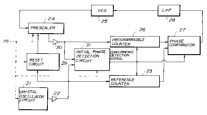
1 DESCRIPTION OF THE PREFERRED EMBODIMENT
Referring to FIG.4, a crystal oscillator
circuit 21 generates an oscillation signal having a
basic frequency, which is input to a reference counter
23 via a buffer circuit 22. The aforementioned power
save signal PS is input to the crystal oscillator
circuit 21, so that it executes an intermittently
oscillating operation. The reference counter 23 is
composed of CMOS transistors, and frequency-divides the
oscillation signal at a predetermined frequency dividing
ratio. A frequency-divided signal is output as a
reference signal. When the reference counter 23
receives a no-signal having a frequency of zero, it does
not receive the oscillation signal having a frequency
higher than zero until an in-phase signal generated by
an initial phase detection circuit 31 is received.
A prescaler 24 is composed of bipolar
transistors, and frequency-divides a signal generated by
a voltage-controlled oscillator 25 at a predetermined
frequency dividing ratio. A frequency-divided signal
from the prescaler 24 is output to a programmable
counter 26. The prescaler 24 receives the power save
signal PS, and is intermittently supplied with
electricity in response to the power save signal PS.
During the operation, current intermittently flows
through the bipolar transistors.
The programmable counter 26, composed of CMOS
transistors, frequency-divides the frequency-divided
signal from the prescaler 24 at a predetermined
frequency dividing ratio. A frequency-divided signal
from the programmable counter 26 is output as a compared
signal. Further, the programmable counter 26 does not
receive a signal having a frequency higher than zero
from the prescaler 24 until the in-phase signal
generated by the initial phase detection circuit 31 is
received.
A phase comparator 27 compares the phase of
2053657
1 the reference signal with the phase of the compared
signal, and outputs a voltage signal based on the phase
difference to the voltage-controlled oscillator 25 via a
lowpass filter 28. The voltage-controlled oscillator 25
generates a signal having a frequency based on the
voltage signal from the phase comparator 27 via the
lowpass filter 28. After the frequencies of the
reference signal and the compared signal become zero,
the phase comparator 27 does not receive the reference
signal having a frequency higher than zero and the
compared signal having a frequency higher than zero
until the in-phase detection signal generated by the
initial phase detection circuit 31 is received.
A reset circuit 29 inputs the signal generated
by the crystal oscillator circuit 21 via a buffer
circuit 22. The reset circuit 29 detects a state where
that the crystal oscillator circuit 21 has started to
oscillate normally, and outputs a reset signal to the
prescaler 24. The reset circuit 29 receives the power
save signal PS, and operates intermittently.
A no-signal hold circuit 30 cuts off the
output signal of the prescaler 24 until the initial
setting operation on the prescaler 24 is executed and
the prescaler 24 starts the stable operation. In this
case, the output terminal of the no-signal hold circuit
30 is maintained in a no-signal state. After the
prescaler 24 starts the stable operation, the no-signal
hold circuit 30 passes the output signal of the
prescaler 24.
When the power save signal PS turns OFF, a
phase comparison/detection circuit 31 inputs the signals
from the prescaler 24 and the crystal oscillator circuit
21, and determines whether or not the signal from the
prescaler 24 rises at almost the same time as the signal
from the oscillation signal from the crystal oscillator
circuit 21 rises. When the signals rise concurrently,
the phase comparison/detection circuit 31 outputs a
-- 10 --
205~6~7
1 concurrence detection signal to the counters 23 and 24,
and the phase comparator 27.
In the state where the entire system is in the
standby mode in which the PLL frequency synthesizer is
intermittently supplied with the power save signal PS,
the power save signal PS is output to the crystal
oscillator circuit 21, the prescaler 24, the reset
circuit 29 and the initial phase detection circuit 31.
These structural elements stop operating each time the
power save signal PS switches to the low level, and
start to operate each time the power save signal PS
switches to the high level.
The crystal oscillator circuit 21 stops
operating each time the power save signal PS switches to
the low level. At this time, the reference counter 23
receives a no-signal which is a signal having a
frequency of zero. Since the reference counter 23 is
composed of CMOS transistors as has been described
previously, the level inverting operation of a CMOS
inverter is not carried out, so that the reference
signal output by the reference counter 23 becomes a
no-signal which is a signal having a frequency of zero.
During this time, energy is not consumed in the
reference counter 23.
The supply of current to the prescaler 24 is
stopped, and thus the prescaler 24 generates a
no-signal, which is input to the programmable counter
26. Since the programmable counter 26 includes CMOS
transistors, it does not the level inverting operation
and does not consume energy. In this state, the
compared signal output by the programmable counter 26 is
a no-signal which is a signal having a frequency of
zero.
Since the phase comparator 27 includes CMOS
transistors, it does not consume energy when receiving
the no-signals from the counters 23 and 26. In
addition, the signal output to the lowpass filter 28 by
2053657
1 the phase comparator 27 when the no-signals from the
counters 23 and 26 are input thereto is in the
high-impedance state. Thus, the PLL frequency
synthesizer is maintained in a pseudo-lock state.
During the time the power save signal is OFF (that is,
maintained at the low level), the voltage-controlled
oscillator 25 continues to oscillate based on the output
signal from the phase comparator 27. In the pseudo-lock
state, the crystal oscillator circuit 21, the counters
23 and 26, the prescaler 24 and the phase comparator 27
do not consume energy.
When the power save signal PS turns OFF and
the crystal oscillator circuit 21, the prescaler 24, the
reset circuit 29 and the initial phase detection circuit
31 start to operate, the reset circuit 29 determines
that the crystal oscillator circuit 21 normally
generates its oscillation signal, and outputs the reset
signal to the prescaler 24, which is then initialized.
After the prescaler 24 is initialized in response to the
reset signal, the no-signal hold circuit 30 outputs the
signal from the prescaler 24 to the programmable counter
26 and the initial phase detection circuit 31.
Hence, the initial phase detection circuit 31
can detect the rise concurrence on the basis of the
stable signals output by the crystal oscillator circuit
21 and the prescaler 24. When the initial phase
detection circuit 31 detects the rise concurrence and
generates the concurrence detection signal, the
reference counter 23, the programmable counter 26 and
the phase comparator 27 start to receive the respective
stable input signals and start to operate. Hence, the
intermittent operation for saving energy consumed in the
PLL frequency synthesizer can be stably performed.
FIG.5 is a circuit diagram of the prescaler
24, the reset circuit 29 and the buffer 30 shown in
FIG.4, and FIG.6 is a circuit diagram of the initial
phase detection circuit 31 shown in FIG.4. The
20~357
- 12 -
1 reference counter 23, the programmable counter 26, the
phase comparator 27, the lowpass filter 28 and the
voltage-controlled oscillator 25 are the same as those
shown in FIGS.l and 2.
Referring to FIG.5, the crystal oscillator
circuit 21 is supplied with the power save signal PS.
When the power save signal PS is at the low level (ON),
the crystal oscillator circuit 21 stops oscillating.
When the power save signal PS is at the high level
(OFF), the crystal oscillator circuit 21 starts to
oscillate. The oscillation signal, labeled XCK, of the
crystal oscillator circuit 21 passes through the buffer
circuit 22 composed of two inverters, and is output to
the reset circuit 29, the initial phase detection
circuit 31 and the reference counter 23 including CMOS
transistors.
The reset circuit 29 has a D-type flip-flop
(hereafter simply referred to as FF) 41, which has a
reset terminal RS receiving the power save signal PS and
a clock input terminal CK receiving the oscillation
signal XCK. Further, the FF 41 has an output terminal
/Q (Q bar) and a data input terminal D, which are
mutually connected. The FF 41 is reset and the output
terminal /Q is switched to a high level when the power
save signal PS switches to OFF. In this state, when the
first oscillation signal XCK is input to the clock input
terminal CK, the output terminal /Q switches to a low
level.
The output terminal /Q of the FF 41 is
connected to one of two input terminals of an FF 42
composed of two NAND circuits. The other input terminal
of the FF 42 is supplied with the power save signal PS.
The output signal of the FF 42 switches to the low level
when the output terminal /Q of the FF 41 switches to the
low level in response to the first input of the
oscillation signal XCK. This state of the FF 42 is
maintained until the power save signal PS turns ON even
2Q53657
- 13 -
1 when the FF 41 operates in response to the oscillation
signal XCK.
In this manner, the FFs 41 and 42 has the
function of determining whether or not the crystal
oscillator circuit 21 starts the normal (stable)
oscillation operation after the power save signal PS
turns OFF. The output signal of the FF 42 is input to
one of two input terminals of a NAND circuit 43, the
other input terminal of which receives the power save
signal PS. The output signal of the NAND circuit 43 is
output, as a preset signal PRES, via a NOT circuit 44.
The present signal PRES is output to a reset signal
generation circuit 45.
The reset signal generation circuit 45 is
composed of four NAND circuits 46 - 49 and five NOT
circuits 50 - 54. The preset signal PRES is input to
the NAND circuit 47, and input to the NAND circuit 48
via the NOT circuit 54.
The NAND circuit 46 and the NOT circuits 50 -
52 form a delay circuit, which outputs the power savesignal PS to the AND circuit 48, and outputs the power
save signal PS to the NAND circuit 47 via the NOT
circuit 53. In this manner, the power save signal PS is
delayed and then input to the NAND circuits 47 and 48.
The delay time of the delay circuit is determined so
that when the power save signal PS switches to the high
level (OFF) from the low level (ON), the high level of
the power save signal PS is input to the NAND circuits
47 and 48 at the same time as the preset signal PRES
switches from the low level to the high level.
When the power save signal PS switches to the
high level (OFF), the low-level signal is applied to one
of the two input terminals 47, and the high-level signal
is applied to the other input terminal 48 thereof. In
this state, when the preset signal PRES becomes the high
level, the output signals of the NAND circuits 47 and 48
switch to the high level. As a result, the reset signal
- 14 -
2053657
1 RES output by the NAND circuit 49 is maintained at the
low level. When the preset signal PRES switches to the
low level from the high level, the output signal of the
NAND circuit 47 is maintained at the high level, and the
output signal of the NAND circuit 48 switches to the low
level. Hence, the reset signal RES output by the NAND
circuit 49 is inverted to the high level from the low
level.
That is, when the power save signal PS
switches OFF, the reset circuit 29 generates the reset
signal RES which rises from the low level to the high
level when it determines that the crystal oscillator
circuit 21 generates the first and normal oscillation
signal SCK. The reset signal RES is output to the
prescaler 24.
The prescaler 24 is composed of a
frequency-divider composed of five FFs 56 - 60 and a NOT
circuit 61, and a reset detection circuit composed of an
FF 62, NOT circuits 63 and 64, and AND circuits 65 and
66. These circuits are formed with bipolar transistors
in order to handle a high-frequency signal.
The FFs 56 - 60 are connected in series. The
output signal of the voltage-controlled oscillator 25 is
applied to a clock input terminal CK of the FF 56 in the
first stage. The FF 60 in the final stage generates,
via its output terminal /Q, an output signal obtained by
frequency-dividing the output signal of the
voltage-controlled oscillator 25.
The FF 62 has a reset input terminal coupled
to the reset circuit 2g via the NOT circuit 63. When
the reset signal RES switches to the high level, the FF
62 is reset. The output terminal /Q of the FF 62 is
connected to its data input terminal D and reset
terminals RS of the FFs 58, 59 and 60. When the reset
signal RES switches to the high level, the output
terminal /Q of the FF 62 switches to the high level,
which resets the FFs 58, 59 and 60.
205~657
- 15 -
1 The AND circuit 65 receives the reset signal
RES and the output signal of the FF circuit 62. When
the AND circuit 65 receives the high-level signal from
the FF 62 after receiving the reset signal FES, the
output signal of the AND circuit 65 switches to the high
level, which is applied to the AND circuit 66. The AND
circuit 66 receives the output signals of the FFs 56 and
57. When both the output signals of the FFs 56 and 57
switch to the high level after the output signal of the
AND circuit 65 switches to the high level, the AND
circuit 66 outputs a high-level signal to the clock
input terminal of the FF 62. In response to the
high-level signal from the AND circuit 66, the output
terminal /Q of the FF 62 switches to the low level, and
is maintained at the low level until the next reset
signal RES is input. The low-level signal via the
output terminal /Q of the FF 62 is input to the
no-signal hold circuit 30 via the NOT circuit 64.
That is, the reset detection circuit of the
prescaler 24 resets the three high-order FFs 58 - 60,
and detects the state where the two low-order FFs 56 and
57 are in the reset state in response to the output
signal of the voltage-controlled oscillator 25. At this
time, the reset detection circuit of the prescaler 24
determines that all the FFs 56 - 60 are in the reset
state, and outputs a signal to the no-signal hold
circuit 30.
The no-signal hold circuit 30 is composed of
two NAND circuits 67 and 68, four NOT circuits 69 - 72,
and an interface circuit 73. The NAND circuit in the
first stage receives the output signal of the reset
detection circuit of the prescaler 24 and the reset
signal RES. When the no-signal hold circuit 30 receives
the high-level output signal of the reset detection
circuit of the prescaler 24 after receiving the reset
signal maintained at the high level, it outputs a
high-level signal to the NAND circuit 68 via the NOT
2053~7
- 16 -
1 circuit 69.
When the NAND circuit 68 receives the power
save signal PS maintained at the high level (OFF) via
one of the two input terminals, and receives the
high-level signal via the other input terminal, it
outputs a control signal CT maintained at the high level
to the interface circuit 73 via the NOT circuit 70.
When the power save signal PS is ON (at the low level),
the reset signal RES is still at the low level, or the
output signal of the reset detection circuit of the
prescaler 24 is at the low level, the control signal
maintained at the low level is output to the interface
circuit 73.
The interface circuit 73 has an input terminal
connected to the frequency-dividing circuit of the
prescaler 24, and an output terminal coupled to the
programmable counter 26 and the initial phase detection
circuit 31 via the NOT circuits 71 and 72,
respectively. When the control signal CT is at the low
level, the interface circuit 73 cuts off the
frequency-divided signal PC from the prescaler 24, and
sets its output terminal to the no-signal state in which
a signal having a frequency of zero is output via the
output terminal of the interface circuit 73. When the
control signal CT is at the high level, the interface
circuit 73 passes the frequency-divided signal fro the
prescaler 24, and outputs it to the programmable
counter 26 and the initial phase detection circuit 31.
That is, the no-signal hold circuit 30
switches to the no-signal state when the power save
signal PS is ON (at the low level), and maintains the
no-signal state until all the FFs 56 - 60 are completely
reset and start to operate normally after the power save
signal PS switches to OFF. When the FFs 56 - 60 starts
to generate the normal frequency-divided signal PC, the
no-signal hold circuit 30 outputs the signal PC to the
programmable counter 26 and the initial phase detection
2053657
- 17 -
1 circuit 31.
As shown in FIG.6, the initial phase detection
circuit 31 is composed of a delay circuit 74, two FFs 75
and 76, a NAND circuit 78, and an FF 79 composed of two
NAND circuits.
The FF 75 has a reset input terminal RS
receiving the power save signal PS, and a clock input
terminal CK receiving the frequency-divided signal PC
transferred via the delay circuit 74. Further, the FF
75 has a data input terminal D receiving the oscillation
signal XCK generated by the crystal oscillator circuit
21. The FF 76 has a set input terminal S receiving the
power save signal PS, and a clock input terminal CK
receiving the frequency-divided signal PC. Further, the
FF 76 has a data input terminal D receiving the
oscillation signal XCK.
The FF 75 switches to the reset state when its
output terminal Q changes to the low level in response
to the switching of the power save signal PS from OFF to
ON, and outputs, via its output terminal Q, the state of
the frequency-divided signal PC obtained at this time in
response to the rise of the oscillation signal XCK.
The FF 76 switches to the set state when its
output terminal /Q changes to the low level in response
to the switching of the power save signal PS from OFF to
ON, and outputs, via its output terminal /Q, an inverted
version of the state of the frequency-divided signal PC
obtained at this time in response to the rise of the
oscillation signal XCK.
That is, when the power save signal PS is ON,
the power supply to the crystal oscillator circuit 21
and the prescaler 24 is stopped, and thus the
oscillation signal SCK and the frequency-divided signal
PC have the no-signal state where the frequencies
thereof are zero. Thus, the FFs 75 and 76 do not
operate. Even when the power save signal PS switches to
ON and the oscillation signal XCK is input to the data
2053657
- 18 -
1 input terminals of the FFs 75 and 76, the FFs 75 and 76
do not operate because the frequency-divided signal PC
is not output.
When the no-signal hold circuit 31 starts to
output the frequency-divided signal PC, the FFs 75 and
76 start to operate in synchronism with the
frequency-divided signal PC. At this time, the FF 75
receives the frequency-divided signal via the delay
circuit 74, the operation starting time of the FF 76
lags behind that of the FF 76 by the delay time of the
delay circuit 74. That is, the FF 75 detects the state
of the oscillation signal XCK which occurs slightly
later than the FF 76 detects the state thereof.
Thus, when the frequency-divided signal PC
rises and the oscillation signal XCK is at the low
level, the output signal obtained at the output terminal
/Q of the FF 76 is at the high level. Thus, the FF 76
waits for the next rise of the frequency-divided signal
PC. At this time, the FF 75 has not yet received the
rise of the frequency-divided signal PC due to the
function of the delay circuit 74. The FF 75 generates
the high-level output signal and waits for the next rise
of the frequency-divided signal PC when the
frequency-divided signal receives the frequency-divided
signal PC in the state where the oscillation signal XCK
switches to the high level before the elapse of the
delay time of the delay circuit 74 and is maintained at
the high level, in other words, in the state where the
rise timing of the oscillation signal XCK and the rise
timing of the frequency-divided signal PC are close to
each other so that the difference between the rise
timings thereof is shorter than the delay time of the
delay circuit 74.
The NAND circuit 78 receives the output
signals from the FFs 75 and 76 and the oscillation
signal XCK. The NAND circuit 78 outputs the low-level
signal to the FF 79, when the output signals from the
2053657
-- 19 --
1 FFs 75 and 76 and the oscillation signal XCK are at the
high level, that is, when the oscillation signal XCK
rises at almost the same time as the frequency-divided
signal PC rises.
The power save signal PS is input to the other
input terminal of the FF 79, which outputs the low-level
signal when the power save signal PS switches to ON.
The NAND circuit 78 changes its state and outputs the
high-level signal to the reference counter 23, the
programmable counter 26 and the phase comparator 27 when
the power save signal PS switches to OFF and then the
NAND circuit 78 switches to the high level. The
concurrence detection signal at the high level is
maintained until the power save signal PS turns OFF.
FIG.7 is a circuit diagram of each D-type
flip-flop used in the prescaler 24. As shown, the
D-type flip-flop is composed of bipolar transistors Q1 -
Q9 and resistors R1 and R2.
A description will now be given of the
operation of the above-mentioned PLL frequency
synthesizer with reference to FIG.8.
When the power save signal PS turns ON in the
standby mode where the power save signal PS alternately
turns ON and OFF, the crystal oscillator 21, the
prescaler 24, the reset circuit 29 and the initial phase
detection circuit 31 are cut off. At this time, the
crystal oscillator circuit 21 stops oscillating and
switches to the no-signal state. Similarly, the
prescaler 24 switches to the no-signal state, and the
no-signal hold circuit 30 switches to the no-signal
state. Thus, the programmable counter 26 receiving the
frequency-divided signal PC and the reference counter 23
receiving the oscillation signal XCK do not operate.
since the counters 23 and 26 are formed of CMOS
transistors, the reference signal and the compared
signal applied to the phase comparator 27 become the
no-signals.
2053657
- 20 -
1 Since the phase comparator 27 is composed of
CMOS transistors and receives no-signals from the
counters 23 and 26, it does not consume energy. During
this operation, the value of the phase comparator 27
which is output to the lowpass filter 28 when the
no-signals are applied to the phase comparator 27 is
maintained in the high-impedance state, so that the PLL
frequency synthesizer is maintained in the pseudo-lock
state. During the time the power save signal PS is ON,
the voltage-controlled oscillator 25 continues to
oscillate by using the value output by the phase
comparator 27.
When the power save signal PS turns OFF, the
crystal oscillator circuit 21, the prescaler 24, the
reset circuit 29 and the initial phase detection circuit
31 start to operate. When the crystal oscillator
circuit 21 starts to operate and generates the first
oscillation signal XCK, the reset circuit 29 recognizes
that the crystal oscillator circuit 21 operates
normally, and generates the reset signal having the high
level. During this operation, the low-level signal is
input to the NAND circuit 67 of the no-signal hold
circuit 30, the frequency-divided signal generated by
the prescaler 24, which already starts to operate in the
state where the initial setting has not yet been
established, is interrupted by the no-signal hold
circuit 30. Thus, the frequency-divided signal PC which
has unstable frequency components is not input to the
initial phase detection circuit 31. Thus, the detection
of the rise timings of the frequency-divided signal PC
and the oscillation signal XCK is not carried out.
Hence, the initial phase detection circuit 31 does not
generate the concurrence detection signal. Although the
reference counter 23 is supplied with the oscillation
signal XCK, the counters 23 and 26 and the phase
comparator 27 do not start to operate because the the
counter 23 is still in the cutoff state.
2() 53~7
- 21 -
1 When the FFs 56 - 60 of the prescaler 23 are
reset in response to the high-level reset signal RES,
the high-level signal is input to the NAND circuit 67 of
the no-signal hold circuit 30, so that the no-signal
hold circuit 30 passes the frequency-divided signal PC
from the prescaler 23.
The initial phase detection circuit 31 starts
to detect the rise timings of the oscillation signal XCK
and the frequency-divided signal after the initial
setting has been executed. When the initial phase
detection circuit 31 recognizes that the oscillation
signal XCK rises at almost the same time as the -
frequency-divided signal PC, it outputs the concurrence
detection signal to the counters 23 and 26 and the phase
comparator 27. In response to the concurrence detection
signal, the counters 23 and 26 frequency-divide the
oscillation signal XCK and the frequency-divided signal
PC at the respective frequency-dividing ratios, and
supply the respective output signals (the reference
signal and compared signal) to the phase comparator 27.
The phase comparator 27 compares the phase of the
reference signal with the phase of the compared signal,
and outputs the voltage signal having a magnitude
dependent on the phase difference.
In the above-mentioned manner, it becomes
possible to rest the reference counter 23, the program
counter 26 and the phase comparator 27 by simply
stopping intermittently operation of the crystal
oscillator circuit 21, the prescaler 24, the reset
circuit 29 and the initial phase detection circuit 31.
Hence, it is possible to save energy consumed in the PLL
frequency synthesizer. Further, it does not take a long
time to pull the PLL frequency synthesizer in the locked
state because the signals respectively latched in the
reference counter 23 and the program counter 26 are not
destroyed.
The frequency-divided signal PC input to the
20536~7
- 22 -
1 initial phase detection circuit 31 has been subjected to
the ini.tial setting procedure. With this arrangement,
it becomes possible to accurately detect the phase
difference between the rise timing of the stable
frequency-divided signal PC and the rise timing of the
oscillation signal XCK. In addition, it becomes
possible to detect the phase difference immediately
after the power supply is turned ON, so that the
intermittent operation on power saving can be stably
executed immediately after the power supply is turned
ON.
The present invention is not limited to the
specifically disclosed embodiment, and various
variations and modifications may be made within the
scope of the present invention.