Note: Descriptions are shown in the official language in which they were submitted.
~'O 90/13879 PCI /AI_i90/00181
a~34
LQCATION MARKER .
Technical Field
The present invention relates to a location marker and in particul~r
discloses a light emitting device that can be used to indica~e the location
of a person or ob~ect.
Conventional light emitting devices that have been used as distress
and location beacons generally utilise a flashing lamp and a battery source
suppling power to the lamp. A switching c~rcuit enables the lamp to flash
pulses of light whlch provide an ind~cation of distress or hazard.
However, these conventional devices suffer the problem that as the
battery source dissipates its energy, the volume of light decreases for
each pulse that is emitted. Also, the electronic circu~t that causes the
lamp to flash can consume a reasonable portion of the energy stored in the
battery and hence reduces the operable period of the light emltting beacon.
Summarv_of the Invention
It is an object of the present invent~on to overcome, or ameliorate
the abovementioned problems through provision of a location marker having
an emitting devlce (for example a light emitting device) that emits a
constant amount of energy for each emission (flash) for the entire life of
its energy supply.
In accordance with one aspect of the present invention there is
disclosed a signalling device comprising: .
a housing enclosing a battery source and an electronic circuit;
switching means adapted to connect said source to said circuit; and
a signal emitter connected to sa~d circuit, said circuit being
adapted to derive energy from said source and to supply pulses of energy to
said emitter, each sald pulse provid~ng substantially uniform energlsing
power during the life of said source.
In accordance with another aspect of the present invention there is
disclosed an electronic circuit~for interconnection between a source of
electrical energy and a load of electrical energy, said circuit comprising:
blocking oscillator means having an input connected to said source
and an output connected to a rect~fier and filter combination, sald
oscillator means converting the voltage of said source to a substantially
higher voltage, the output of said combination supplying sald load;
t~mer means supplied by said source that outputs to an electronic
~ ... ... ..... . , - .,, . ,,.. , . .. ~, ~, . . .,,-. .
~O 90/13879 PCT/AU90/00181
r ~
isolat10n devlce a triggerlng pulse at intervals proportional to the
voltage of sa~d source said isolation device interconnecting said tlmer
means wlth a trigger device sald trigger device being connected to sald
higher voltage and adapted to cause a pulse of electrlcal energy to be
dissipated by sald load in response to said trigger pulse the energy
disslpated in said load being substantially equal for each consecutive
pulse.
In accordance with another aspect of the present ~nvention there is
disclosed a lens formed of translucent diffusing plastics material said
lens hav~ng a substantlally cylindrical body the interlor of said body
belng adapted for the insertlon of a lamp one end of said body being
sealed by said plastics material with said seal being of such thickness so
as to allow for the formation within said seal of a conical or domed
structure sald lens further comprising a flange formed at the other end of
sald body through which said lamp can proiect into said body said
structure and saSd flange substantially increas~ng the d~sperslon of llght
em~tted by sald lamp from sald lens.
In accordance with another aspect of the present invention there is
disclosed a swltch assembly for select~vely connecting and disconnecting
two pairs of terminals sald assembly comprlsing:
two contact pads arranged on one surface of a contact block each of
sald pads adapted to contact ln a first pos~tlon two adjacently located
termlnals;
a magnetlcally operable swltch located ln said contact block that
provldes for electrical connection and disconnection between said contact
pads;
a boss rotatably connected to said contact block and rotatable
between two posltions one of said posltions allgning a magnet located
wtthln said boss with sald magnetically operable switch;
sald boss and said contact block being adapted to rotate together
such that each said contact pad contactsi in a second position to
adjacently located terminals.
The adaptatlQn of the present invention to a radio frequency
transmltting dlstress beacon is also disclosed.
Brief De~crlptiQn of the ~rawinas
A preferred embodiment of the present invention will now be described
wlth reference to the drawlngs in which:
,
.
WO 90/13879 PCI /AIJ90/00181
- 3 - 2~r~
F~g. 1 lllustrates a perspective view of a devlce of the preferred
embodiment;
Fig. 2 illustrates a longitudinal cross sectlon of Flg. l;
Fig. 3 is a block diagram of the complete electronic clrcult;
Fig. 4A and 4B are circuit diagrams of two embodiments of Fig. 3;
Figs. SA and 5B are graphs that show the performance of two
embodlments of the present invention;
Fig. 6A is an exploded perspective ~llustratlon of the swltch cap
assembly;
Fig. 6B ls a plan view of the contact block of Fig. 6A;
Fig. 6C is an lnverted plan view of the switch boss of Fig. 6A;
Figs. 7A to 7D illustrate different connectlons made by the operation
of the switch of Flg. 6 in various posltlons;
Fig. 8 ls a cross section of the lens;
Fig. 9 lllustrates the casing surface configuration.
Fig. 10 is a vlew s~m~lar to Fig. 2 showing an embodiment of an RF
transmittlng locatlQn marker; and
F~g. 11 ls a v~ew sim~lar to Fig. 1 but showlng an alternatlve
antenna arrangement to that of Fig. 10.
Best and Other Modes for Carrvinq Out the Invention
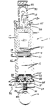
The locatlon marker 10 lll~strated in Fig. 1 comprlses a casing 11
that has attached to one end a lens 50 that encloses a lamp 12. At the
other end of the casing 11 is a switch cap assembly generally ind~cated at
30 that can be operated to cause the location marker 10 to flash. The
casing li ls preferably provided with an external configuration comprising
tetrahedon structures 13 that prevent slippage when held by an operator.
Also the locatiQn marker 10 can be provided with a metal ring 14 for
attachment to an object or the clothing of a person.
Flg. 2 illustrates a detailed longitudinal cross section of the
locatlon marker lO of Fig. 1. Enclosed wlthin the casing 11 is an
electronic circuit 60 that interconnects batteries lS to the lamp 12. The
electronic circuit 60 is suspended wlthin the casing 11 by a fllllng
material 17 that prevents damage to the electronic circuit 60 through shock
or vlbratlon. The flll~ng material 17 can be any substance commonly used ~;
for this purpose such as silicone rubber or epoxy resin.
The caslng 11 is div~ded in two portions by a wall 18 that separates
the filling material 17 from the battery compartment 16. The wall l$ can
:
WO 90~13879 P~/AU90/OOlXl
z~ 34 - ~-
be manufactured of epoxy resins bakelite or any other resllient
substance.
The preferred embodiment utilises four AA-size batteries 15 only two
of whlch are illustrated in Fig. 2. The batteries 15 rest on a spring
plate 19 that comprises springs 20 each of which providing connection to
one termlnal of each of the batteries 15. Electrical connections 21
between the springs 20 and the electronic circuit 60 pass through the
spring plate 19 and the wall 18.
The sw~tch cap assembly 30 comprises a contact block 35 and switch
boss 34 and is attached to the casing 11 by a threaded connection formed of
screw thread 22 on the caslng 11 and corresponding screw thread 31 on the
contact block 35. The threaded connection forms a waterproof seal between
the exterior of the locatlon marker 10 and the interior of the casing 11.
Contact pads 32 and 33 provide connection to the other ends of the
batteries 15.
The electrical operatlon of the location marker 10 will now be
descrlbed with reference to Flgs. 3 and 4 that lllustrate in detail the
electronic clrcult 60. Flg. 3 shows ln block diagram form the general
arrangement of the electrical clrcultry of the location marker 10. The
batterles 15 provlde electrical power vla the switch 30 to the electronlc
circult 60. The electronlc circuit 60 comprlses a chopper 61 that provides
pulses of electrical energy to a converter 62 which transforms the battery
voltage to a substantlally hlgher voltage. Thls substant~ally higher
voltage ls then flltered by rectlfler and storage element 63. A timer 64
connected to the batterles 15 via swltch 30 provides triggerlng pulses to a
trigger circuit 65 that triggers the lamp 12 lnto a conductlve state which ~:
draws energy from the rectifier and storage element 63.
One preferred embodiment of the electronic clrcuit of Fig. 3 is
illustrated in Fig. 4A. Transformer Tl resistor Rl and transistor Ql
together form the chopper 61 and converter 62. These components create a
blocklng oscillator that provldes a high voltage to the anode of diode Dl.
Together dlode Dl and capacitor Cl form the rectlfier and storage element
63 anci provlde a ~lltered high voltage that is connected to one input of
the lamp 12.
Integrated circult IC2 is the timer 64 that provides trigger pulses
to an opto isolator ICl. The time between the trigger pulses being
determlned by capacitor C3 and the voltage across IC2. As such the period
W O 90/13~79 ~ ~ /AU90/U0181
between trigger pulses increases as the battery voltage decreases as
occurs w~th extended usage. The opto isolator ICl commun~cates the trigger
pulse to the swltch SCRl that together wlth transformer T2 resistor R2
and capacitor C2 forms the trigger circu;t 65 and relays the trigger
pulse to the lamp 12.
The lamp 12 is preferably a xenon lamp that is capable of being
pulsed repeatedly over extended perlods of time.
The operation of the electronic c~rcult 60 of Fig. 4A wlll now be
described. In~tially all voltages and currents wlthin the circuit 60 are
at zero. When the batteries 15 are flrst connected across the circuit 60
upon closure of the sw~tch 30 current lnit~ally flows from the pos~tive
terminal of batter1es 15 lnto the emitter of Ql to bias the base of Ql via
wlnding Fl and resistor Rl. Ql then conducts from emitter to collector
through winding ~1. The flow current through Wl first opposes current flow
in Fl and once those currents achieve correspondlngly proportionate
magnitudes the b~as of Ql provided by Fl ls reversed switching Ql off. Ql
swltching off causes back EMF of transformer Tl to output a current through
Dl to charge capacitor Cl. Once the back EMF is dissipated the blocking
oscillator formed by Tl Ql and Rl reverts to it s initlal state.
Timer IC2 prodùces a sharp narrow pulse of repetltion rate
proportional to the battery voltage and the value of capacitor C3. The
period between the pulse can be determined by the equat~on
T KC3
V ':
where
T ~ perlod between each pulse
V - the supply voltage
K - constant determined by circuit parameters.
The pulse provided by IC2 being short and sharp is isolated from
the trlgger devices by opto-isolator ICl. Furthermore ICl provldes for
further shap~ng of the pulse that lmproves it s sharpness. Due to the
sharp quality of the~pulse the oscillation of the blocking oscillator
61 62 is not impeded should there be insufficient energy stored in Cl to
fire the lamp 12. ICl communicates the pulse to SCRl which then switches
on. The charge stored on C2 together with the current flowing through SCRl ~
`: :
:,
.
WO 90/13879 ` PCl/AU90/00181
lnduce a hlgh voltage pulse of approximately 300 volts that is supplied to
the lamp trlgger via T2.
An alternate embodiment of the electronic circult 60 ls shown in Fig.
4B as clrcuit 70. Components are as previously described but the trigger
clrcuit 65 has been rearranged. This embodiment provides marginally lower
voltage triggertng and hence longer operation than the circuit 60 of Fig.
4A.
The electronic clrcults 60 and 70 have been optimlsed to ensure that
maximum energy is transferred from the batteries 15 to the lamp 12. For
example the resonant frequency of the feedback winding Fl of transformer
Tl ls matched with that of the resistor Rl and the impedance presented by
translstor Ql. This eliminates the need for a bypass capacltor on the base
of translstor Ql as is normally requ~red in chopper circults used for
photographic lamps. As such the energy dissipated in such a bypass
capacitor ls not wasted in the electronic circuit of the Fiss. 4A and 4B.
Also the trigger circu~t allows for the blocking oscillator converter to
function uninterrupted. This provides for capacitor Cl to be continu~lly
charged so that a constant amount of energy can be transferred to the lamp
12. Other non preferred clrcuits place the load switchlng device SCRl
dtrectly off the converter 62 ~Tl). This unpreferred form requires high
gate currents on SCRl to ensure trigger7ny of the device and hence
illumlnation of the lamp 12.
The electronic circults 60 and 70 are further optimised ~n the use of
opto coupler ICl that provides a short sharp triggerlng pulse to SCRl and
also provides isolation protection for the timer 64 (IC2) from voltage
surges at the trigger clrcuit 65 (SCRl).
The opt1mlsation of the electronic eircuits 60 and 70 provide for
substantially the same amount of energy to be transferred to the lamp 12
with each trigger pulse. This occurs irrespective of the age and condition
of the batterles 15 and the period between the trigger pulses. As such a
constant volume of llght is emitted by the lamp 12 for the entlre life of
the batterles 15. ..
F1gs. SA and 5B illustrate the performance of two forms of the
electronic circuit 60 over a period of time. It will be seen from each of
the graphs in Figs. 5A and 5B that the period between the flashes of the
lamp 12 increases as the batteries deteriorate over time. Fig. 5A
illustrates a normal flash rate.commencing at approximately five seconds
.
.
,
WO 90/1387~ PCI`/ A U90/00 181
between each flash and Fig. 5B illustrates a rapid flash rate commencing at
approx~mately 2.3 seconds between each flash. The varlation in flash rate
being pravided between each case by changing the value of capacitor C3 in
Flgs. 4A or 4B.
The location marker 10 is operated by the actuation of the swltch cap
assembly 30. The assembly 30 is shown in an exploded perspective drawing
at F~g. 6A. The assembly 3Q comprlses a switch boss 34 that is rotatably
mounted on a contact block 35 uslng a sp~got 36. The spigot 36 is
preferably manufactured of stainless steel. The assembly 30 is res~liently
held together by spring 43 and nut 44. The switch boss 34 has finger
scallops 46 formed in it s circumferential surface to aid in grasping and
turnlng the boss 34 to operate the location marker 10. The contact block
35 has on lts lower face contact pads 32 and 33 that each make connection
with two of the four batteries 15. The contact pads 32 and 33 are
substant~ally hemispherical rings that provlde for the entire contact block
35 to be rotated across the surface of the four batteries 15.
Located within the contact block 35 and not illustrated is a
magnetically operable swltch which provides electrical connection and
dlsconnection between the contact pads 32 and 33. The magnetically
operable swltch ~s preferably a Reed Sw~tch or a Hall Effect Device.
The switch boss 34 compr~ses posts 37 and 38 that protrude from an
unders~de face of the switch boss 34 and mate wtth two holes 39
(~llustrated in Fig. 6B) located in the upper surface of the contact block
: 35. W1th reference to F~gs. 6B and 6C the holes 39 define two positions
of rotation of the switch boss 34 over the contact block 35 about the
spigot 36. Also located in the underside face of the sw~tch boss 34 and
between the posts 37 and 38 ls a magnet 40 that operates the magnetically
operated switch located in the contact block 35!
A vapour and water-tight seal is provided when the contact block 22
1s screwed lnto position on the thread 22 of the casing 11. The seal is
malntalned by a O-ring 41 located in a corresponding groove 42 as seen in
F~g. 2 of the contact block 35 adjacent its thread 31.
Those sk~lled in the art w~ll understand that when the switch cap
assemply 30 is assembled the switch boss 34 will be rotatable about the
sp~got 36 so that the magnet 40 can actuate the magnetically operated
switch located ln the contact block 35. This is a normal mode of operation
of the location marker 10 and the electrical connections prov~ded by this
:, '
.
W O 90/13879 PCT/AU90/oo
9~ - 8
normal mode are depicted in Figs. 7A and 7B. Fig. 7A illustrates the
locatlon of the contact pads 32 and 33 with the batteries 15a 15b, 15c and
15d, that provide power to the electronic circuit 60. Rotation of the
swltch boss 34 about the contact block 35 thus will close the magnetically
operable switch indicated diagrammatically at 45 in Fig. 7B and complete
the electrical ctrcuit. Fig. 7B illustrates the connection of the
batteries of the preferred embodiment. Spr~ng plate connections 23 and 24
connect terminals of adjacent batteries (15a,15b) (15c,15d) at the spring
plate 19 to which electrical connections 21 are made. The polarities
indicated on batterles 15a, 15b, 15c and 15d in Figs. 7A and 7C are those
at the contact block 35 end of the battery compartment 16.
~ hen using four standard AA batteries as the batteries 15, the
preferred embodiment provides a power source of approximately three volts.
The arrangement of the contact pads 32 and 33 provide for the switch
assembly ~0 to be operated in an emergency mode in which the magnetically
operable switch ~s by-passed. In this mode of operation, the entire switch
cap assembly 30 is rotated through 90 about the casing 11. A counter
clockwlse rotation causes the contact pads 32 and 33 to be arranged as
lndicated in Fig. 7Co The corresponding electrlcal connection of the
batterles 15a, 15b, 15c and 15d ~s deplcted in Fig. 7D~ It is seen from
F~g. 7D that the operatlon of the magnetically operable switch does not
impede the connection of the batteries lS to the electronic circuit 60. A
clockwlse rotatlon of the assembly 30 produces the same electrlcal result,
only lnterchang~ng the posltlons of the batteries 15a, 15b, 15c and 15d,
from those illustrated in Fig. 7D~
It will be realised by those skilled in the art that the operation of
the switch cap assembly 30 does not alter the vapour and water-proof
securlty of the interior of the casing 11 and thus effectively protects the
batter1es 15 and electronic clrcuit 60. This feature is afforded by the
use of the magnetically operable switch sealed within the contact block 35.
The locatlon marker 10 ls provided with a lens 5Q that disperses
light produced by the lamp 12. Referring to Fig. 8, the lens 50 is shown
ln longitudinal cross sectlon. Lens 50 comprises transparent or preferably
translucent plastics material formed by injection moulding or machining.
The lens 50 comprises a substantially cylindrical body 51 that has a hollow
lnterlor 52 centered about the longitudinal axis of the body 51. The
hollow inter~or 52 allows for the insertion of the lamp 12 into the lens
.
.
WO 90/13~79 PCll`~AU90/OOlX1
~ 9 ~ 2 ~ S~
50. Preferably, in the closed end of the hollow interior, a cone or dome
53 is formed which affords increased dispersion of the light through the
lens. It is considered that for the purposes of locat~ng persons in
distress by means of a light beacon, the dispersion of light provided by
the light beacon is as important as the intensity of the light provided by
the beacon. The cone of dome 53 can be formed by further boring of the
~nterior 52 or, as illustrated in Fig. 2, by double-shot injection moulding
of a plastics material of dlfferent refractive index to that used ~n the
cylinder 51 of the lens 50. The base of the lens S0 comprises a flange 54
that encloses the end of the casing 11 as seen in Fig. 2. The end of the
casing 11 is sealed by an 0-ring 55 and corresponding recess 56 formed on
the flange 54. The lens S0 is also bonded to the casing 11 by a solvent
weld or other sultable means.
In an alternative embodiment, the lens 50 can have shoulders 57
between the cylindrical body 51 and flange 54 that add to the dispersion of
llght from the lamp 12. Also, the lens can be coloured to provide for
group ident~f~cat~on when various location markers 10 are ln use at any one
point in time.
The casing 11 is an in~ected moulded cylinder that has an external
configuration formed of tetrahedon or pyram~dal structures 13. The rows of
tetrahedon structures 13 are interleaved as indicated in Fig. 9 with the
spaclng between these rows being tailored for maximum shedding of
detretious material such as mud, snow and ice. The result being that the
casing 11 is more readily grasped so that the switch cap assembly 30 can be
operated even under the most testing circumstances. This is due to the
interaction of the grasping hand, or gloved hand, causing a shearing action
agalnst the tetrahedon structures 13 that chann21s detretious material
between the adiacent 1nterleaved tetrahedons that transports such material
away from the casing 11.
The casing 11 is preferably manufactured of plastics material that
has a high impact resistance and can be used within broad temperature
ranges. Preferably, the plastics material is Noryl N225 (Registered Trade
Mark) which 1s useful from -50C to 120C.
Also, 1t is preferred that the posts 37 and 38 and spigot 36 be
manufactured of 316 stainless steel. The contact pads 32 and 33 and
springs 20 are preferably manufactured of nickel silver which affords low
electrtcal res~stance and substantial resistance to corrosion.
'~
.
, . ~ ... . . . .... . . . . . . .. . . . . . . . . .... .. . . . . . . . . . . . . . .
W O 90/13879 pcr/Au9o/ool81
-- 10 -
The location marker 10 has achieved a safety rating of Class 1 Zone 0
and Australian Standard AS2431-1981 Electr~cal Equipment for Explosive
Atmospheres. Also the electronic circuit 60 70 when encapsulated meets
the same standard. Also such a device is waterproof to 150 metres.
The present invention has advantages over prior art devices in that
the swtich cap assembly 30 is hermetically sealed and thus protects the
electr~cal components of the device as well as having an emergency by-pass
posltion that can be used if the normal switch fails. Such a locatlon
marker is extremely rugged and is suitable as a distress beacon or as a
location device for use in search and rescue.
The location marker 10 has negative buoyancy and thus can be used by
underwater divers as top and bottom markers on a diving line.
Alternatively the location marker 10 can be prov~ded Witil a float collar
(not illustrated) of positive buoyancy that fits over the casing with an
interference fit and provides for buoyancy of the marker such that the
cylindrical body 51 of the lens 50 protrudes from the water wlth the flange
54 belng slightly beneath the surface of the water. As such the
posltioning of the flange 54 within the water adds to the dispersion of
llght afforded by the lens 50. Alternatively depending upon the location
of the collar about the casing 11 the location marker ~s buoyant w~th the
lens 50 pointing downwards into the water. Such a use ls preferred by
underwater dlvers in provlsion of a top-marker .
The foregoing describes a number of embodiments o~ the present
inventlon and other embodiments obvious to those skilled in the art can
be made thereto w~thout departing from the scope of the present invention.
For example lithium batteries can be used where long shelf life is
required ~n l~feboats for example. At the date of this application
AA-s~ze lithium batteries are not available however C size lithium
batteries can be used by revising the arrangement of the contacts 32 and 33
and by ~nsertlng a collar around the batteries to retain them in the
battery compartment 16.
Also the location marker 10 and electronic circuit 60 can be adapted
to pulse a radio frequency transm~tter and an antenna in place of the lamp
12. Fig. 10 ~llustrates such an embodiment where a revised low voltage
electric circuit 80 similar to circuits 60 and 70 pulses a radio
frequency transmitter 85. The transmitter 85 preferably operates in the
VHF or UHF bands at appropriate distress/emergency frequencles. The
W O 90/13~7~ PCr/AU90/0~
1 1 - 2~ 34
transmitter 85 drives an antenna 90 that can be provided in place of the
lamp 12 within the lens 50. Alternat~vely as ~llustrated in Fig. 11 the
lens 50 is replaced entirely by an omnidirectional antenna 95 which is
sealed to the casing 11 in the same manner as the lens 50. Due to the size
of the antenna 95 frequencies of tranmission in the UHF band are
preferred. Such antenna 90 and 95 together with the RF transmitter 85 will
be known to those skilled in the art. This embodiment will however be
distlnguished from prior art transmitters by maintaining a substantially
constant transmltted power for each pulse over the life of the batteries
15.
Also the lens 50 can be provided with an infrared sleeve adapted to
cover the lens 50 to prevent the escape of visible light but transm~tting
infrared light. Alternatively the lens 50 can be manufactured of
materials transparent to infrared light but not visible light.
. .
,