Note: Descriptions are shown in the official language in which they were submitted.
I)UAL-CODED DATA Cl)MPARATOR
BACKGROUND OF THE INVENTION
The present invention relates generally to comparators, and more
particularly to a comparator for comparing dual-coded data, such as can be
5 used for fast address comparison in computer systems, for testing and
diagnosis of software, or in digital control circuits for comparison of reference
and actual values.
In some hardware comparators, the data is checked directly, bit by bit,
using gates or comparators. However, with the bit width of data words used
10 in current computer systems, this leads to a correspondingly large number of
components. In many instances, these large numbers of components cannot
be tolerated, because of the resulting space requirement.
f~ ~S~ ~aiel~t N~3scloses a comparator provided with
i~ memory in which characteristic data are stored at specific addresses, which
C ~ /D~ 15 map the comparison data in question so that the data can be output byC~6f 1 ,'c~f address control. By dividing the address lines into individual groups, the
6 ~ known device achieves a reduction in the required address space, and a 2-bit
i i 3 ~, ~ 1 7 ~
wide version of the memory makes it possible to provide information as to
whether a currently accessed address is equal to or greater than the~J61< ~/J 20 comparisonaddress.
The present invention is directed to the problem of further developing
hardware comparators for comparing dual-coded data by reducing the
number of required components and by expanding their area of application.
" . .
` 2~3~6
-2-
SUMMARY OF THE INVENTION
The present invention solves this problem by distributing the address
lines evenly in groups among several 1-bit wide memory chips, in which
characteristic d~ta are stored relative to a specific address mapping the
5 comparison data item. This characteristic data can be output with address
control by a second data item to be compared with the comparison data item,
in that the data output of each memory is connected with the read comrnand
input of the memory which is assigned to the address line group with the next
higher value.
B~rEF DESCRIP~ION OF THE DRAWINGS
FIG. 1 illustrates the basic structure of a ~AM.
FIG. 2 depicts a known address comparator with group-type division of
the address lines.
FIG. 3 shows an example for group-type evaluat;on of partial data
according to the present invention.
FIG. 4 illustrates a comparator according to the present invention for
eight addresses.
FIG. S depicts a basic element of a reference/actual value comparator
20 according to the present invention outputting the amount and the sign of the
deviation.
FIG. 6 shows a known embodiment for a reference/actual value
comparator which can be used in two-point or three-point controls.
FIGs. 7 and 8 depict the corresponding, improved embodiment
according to the present invention.
FIGs. 9 and 10 illustrate ~wo embodiments of reference/actual value
comparators according to the present invention outputting amount and sign of
the deviation, as well as group-type division of the address lines.
FIG. 11 shows a numerical example for formation of the deviation.
FI&. 12 depicts an implementation of a referencetactual value
comparator according to the present invention with more than two address
line groups.
.
., ~ ., :,
-- : , ~,, , :
,
2 ~
-3 -
DETAILED DESCRIPTION r
FIG. 1 shows the basic structure of a ~^bit wide memory using the
example of a read-write memory also designated as Random Access Memory
(RAM). The memory has three address inputs, to which address lines A0,
5 A1 and A2 are connected. These address inputs act on the inputs of an
internal decoder, which decodes the 23 possible signal combinations of the
address lines A0 to A2 into eight addresses 0 to 7, by outputting an access
signal for one of the memorS cells designated as MEM at only one of its
eight output lines for each individual signal combination. The content of the
10 memory cell selected by its address access can either be output ~y means of a read command RD, via a data gate OUT, to the output line D, or, by
activating the data gate IN, the signal on the data line D can be taken over
into this memory cell by means of a write command WR, i.e. it can be
written to. If, as shown, the address lines A2 and A1 have the value logic "1"
15 and the address line A0 has the signal status logic "0" and if the value logic
"1" is applied to the data line D, then this value is written into the memory
cell with the address 6, using the write command WR. On the other hand, if
the memory is charged in this way, and if the data gate OUT is activated
using the read command RD, the signal logic "1" is only issued if the address
20 lines have the signal combination shown, namely dual ~, applied to them, and
every other signal combination of the address lines A0 to A2 will result in the
value logic "0" when the memory is read out. In this way, it can be
determined whether any desired dual-coded data item which is applied to the
address lines of the RAM agrees with the comparison data item, i.e. if data
25 which is characteristic for the equivalence of the two data, in this example
logic "1", is stored at an address determined by the comparison data item.
The comparison of two data is reduced, so to spealc, to a comparison of
location in the RAM.
FIG. 2 shows a known address comparator, in which the number of
30 addresses to be decoded is reduced. This comparator has z 1-bit wide RAMs
RAM1 to RAMz. The n-address lines required for formation of the memory
addresses are divided in groups among the individual RAl~Is, so that z groups
- . .
%~;5~
-4-
of different value, with n/z address lines each, are passed to the RAMs~
Thus, the n-digit data to be compared is divided into z partial data, each of
which is n/z-digit and is decoded in its own R~I, the data output of which is
only logic "1", i.e. "true" at the partial address assigned to the partial
5 comparison data. The data outputs of all the RAMs are connected with the
inputs of an AND gate 2, the output signal K o which has the value logic "1",
if the value logic "1" occurs as the criterion of agreement of the comparison
data item with the data item to be compared, in groups at the assigned data
output D1 to I)z in each case. The memory volume to be built up is reduced
10 to ~.2~ with this arrangement. Therefore, the greater z is selected to be, the
smaller the required memory volume becomes, but the number of required
memory modules increases since this number is proportional to z. As a rule,
a comprornise will have to be reached between ~he smallest possible
expansion of the individual memory chips and minimization of the number o~
lS memory modules.
FIG. 3 serves to illustrate the group-type evaluation of the partial data
of an address comparator according to the present invention, showing an
easily understandable example. In the right part of ~IG. 3, the value range
of 0 to 15 which can be represented with four address lines A0 to A3 is
20 shown with the related combinations of signal status of these address lines. If
the address lines A0 to A1 are combined into a group with lower value, with
the weight 4 ~ 1, and the address lines A2 to A3 are combined into a grollp
with highe~ value, with the weight 4~ = 4, and if the address value is allowed
to run from 0 to 15, then four bit patterns BM1 to BM4 result for the lower-
25 value address line group ~0, A1, which repeat cyclically three times. Thesame ~it patterns occur in the same cyclical sequence also for the higher-
value address line group A2 and A3, but for a complete cycle of these bit
patterns in the lower-value address linè group, the bit pattern of the higher-
value address line group remains the same. Analogous to a mechanical gear
30 translation of 4:1, where for every four revolutions of the one gear wheel, one
revolution of the other one occurs, the bit pattern sequence ~M1 to BM4
occurs for the lower-value address line group A0, A1 per bit pattern of the
" ~ ~ -
-s-
higher-value address group A2, A3. Therefore it is possible, by taking into
consideration the weight of the groups, to decode 16 addresses ~Nith two
RAMs, each of which only has to decode four addresses. In the left part of
FIG. 3, two RAMs RAM1 and RAM2 are assigned to the address line groups
5 A0, A1 and A2, A3. As in FIG. 1, the value 6 is assumed as the comparison
data item, so that the value 1 is stored at the corresponding partial address,
as indicated with shading. This partial address is 2 in RAM 1 and 1 in
RAM2. In equivalent modification of FIG. 2, the AND link of the two data
outputs is brought about in that the data output of the ~AM assigned to the
10 lower-value address line group is connected with the read control input RD
of the RA~I assigned to the higher-value address line group and sllpplies the
read command in this way. Therefore the need for an AND gate is
eliminated. If the value of the data item to be compared, which is on the
address lines A0 to A3, now starts to increase from 0 to lS, then the data
15 output at RAM1 for the lower-value address line group will assume the logic
value "1" at the values 2, 6, 10 and 14 (A0=0, A1=1). The value logic "1"
can be read out of RAM2 only if A2=1 and A3=0 is also true, which is the
case when the value of the data item to be compared is 6.
The principle shown in FIG. 2 and explained using FIG 3 can be
20 implemented ~or any bit width, i~e. for any number o~ positions n of the dual-
coded information and for any number of groups z, and is essentially based
on dividing an n-digit dual mlmber into z groups with n/z digits in each case,
and processing it in a 2' number system.
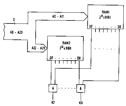
FIG. 4 shows an embodiment of the present invention with which an
25 address comparison with regard to eight reference value addresses is
supposed to be undertaken for an address bus with 24 address lines A0 to
A23. If a single memory is used, it would have to decode 224Zl6 lo6 in this
example. According to the present invention, the 24 address lines of the
address bus 3 are divided in half between RAM1 and RAM2, which are each
30 8 bits wide. According to the principle explained in FIG. 3, the characteristic
information for a specific partial address, namely logic "1", is stored in the
. ~ .
. - : :
' 3 ~ ~
-6-
columns belonging to the data outputs D0 to D7 of each of the two RAMs.
The data output lines D0 to D7 belonuing to a specific address are passed to
the inputs of AND gates, and the coincidence signals K0 to K7 then occur at
the outputs of these AND gates during inquiry, if the address on the address
5 bus agrees with one of the specific addresses. The arrangement according to
FIG. 4 corresponds to the arrangement according to FIG. 2 with n = 24 and
z = 2, as well as a multibit-width version of the memory chips, corresponding
to the multiple comparison.
For reference/actual value comparison in digital control circuits, it is
10 necessary not only to determine the agreement between a reference value
address marked in the memory with the address applied, which corresponds
to the current actual value in each case, but rather, for two-point or three-
point controls, a quali~ative statement whether the current actual value is
greater or less than the reference value, and, for quasi-constant controls, also15 a quantitative statement as to the size of the reference/actual value
difference, i.e. the deviation, is also required. The basic memory structure
for this is shown in FIG. 5. The characteristic information entered into a
memory line assigned to the reference value address is emphasized with
shading. The colurnns of a RAM, designated as RAM, assigned to the two
20 data outputs D0 and Dl, serve for an inqui~y of data as to how the actual
value is behaving relative to the reference value. At the reference value
address, this characteristic in~ormation consists of the logic value "11", for
addresses which are less than the reference value address, the logic value "01"
is entered, and for addresses which are greater than the reference value
25 address, the characteristic information consists of the value "ûO". The
inve~ted signal of the data output line D1 and the signal of the data output
line D0 are passed to an AND gate 4, so that a "1" signal occurs at its output
designated as al, if the actual value address is less than the reference value
address, i.e. if the difference between the reference value and the actual
30 value is positive. At the output of the AND gate 5, the inputs of which are
connected with the data lines D0 and D1, a "1" signal appears if the actual
value address agrees with the reference value address, while a "1" signal
3 Q ~
-7-
occurs at the output of the invertor connected with the signal of the data
output line D0 on the input side, if the actual value is greater than the
reference value, i.e. if the deviation has a negative sign.
The RAM designed for n address lines A0 to An-1 is furthermore
5 expanded by a column width which corresponds to the number of address
lines, and in each line assigned to an address, its relative distance from the
reference value address is entered in dual-coded form. Thus, the value of the
lines adjacent to the reference value address is 1, that of the next lines is 2,etc. With a write command WR, the RAM can be read OUt line by line,
10 corresponding to the applied address, with the amount l ~ l of the deviation
then being received at the data outputs D2 to Dn+ 1, "1" signals being
received at the outputs al or a3, depending on the sign of the deviation, or a
"1" signal being received at the output a2 if the reference value and actual
value are in agreement.
FIG. 6 is an example of the structure having a reduction in the
addresses to be decoded by dividing the address lines into three groups for
digital two-point or three-point control. RAM1 to RAM3 are two bits wide
and the characteristics are stored in their memory cells in the manner shown
in FIG. 5. Therefore it is possible to determine, per address line group,
20 whether the partial reference value address assigned to it is greater than,
equal to or less than the corresponding partial actual value address. The
ev~luation of the partial data relating to the individual group takes place by
me;~ns of a logic circuit consisting of the gates 7 to 14, taking into
consideration the weight of the individual groups. As a matter of principle,
25 the group with the highest value determines the sign of the deviation, and if an agreement between the reference value address and the actual value
address is found for this group, this function passes on to the group with the
next lower value. Therefore, the AND gates 8 and 9, which correspond to
the AND gates 4 and 5 in FIG. 5, are used to check whether the actual value
30 is less than the reference value. If this is the case, a "1" signal occurs at the
output of the O~ gate 13. Since the output of the AND element 9 then has
a "0" signal at the same time, the AND gates 10, 11 and 12 are blocked with
3 ~ ~
this "1" signal. If, on the other hand, the actual value address at the highest-value groups assigned to RAM3 is greater than the reference value address
there, the output signals of the AND gates 8 and 9 are both logic "0", as is
the output signal of the OR gate 13 and the output signal of the AND gate
5 12, so that the output of the AND gate 14 is a "1" signa}. If, on the other
hand, there is agreement between the actual value and the reference value at
the highest-value group, then only the output signals of gates 8 and 9, will
have a "1" signal, with which the AND gates 10, 11 and 12 are made ready to
undertake evaluation of the sign, using the data output signals D0 and D1 of
10 the next lower address line group, in precisely the same manner: If D1 = 0
and D0 = 1, then the reference value address of the address line group
assigned to RAM2 is smaller than the reference value and a "1" signal
appears at the output of the AND ga~e 10 and therefore also that of the OR
gate 13, while the "0" signal which occurs at the output of the AND gate 7 at
15 the same time blocks the ~ND gates 11 and 12. If agreement between the
reference value and actual value is achieved also at the address line group
assigned to RAM2, a "1" signal appears at the output of the AND gate 7,
which causes the determination of the sign of the deviation to pass on to the
group with the lowest value, until finally a "1" signal appears at the output of20 the AND gate 12, if agreement between the reference value address and the
actual value address prevails in all three RAMs, i.e. the deviation has become
zero.
FIG. 7 shows an advantageous embodiment of the reference/actual
value comparator shown in FIG. 6 according to the present invention. The
25 logic circuit, which consists of individual gates 7 to 14 there, is implemented
using a read-only memory 15 in the form of a PROM (Programmable Read
Only Memory). The data outputs D0 and D1 of the indi~idual RAMs,
RAM1 to RAM3, are connected with the inputs el to eG of the PROM 15,
and the connection between the signal status of these inputs and the signal
30 status of the outputs al, a2 and a3 of the PROM 15 is shown by the related
truth table in FIG. 8. In the right half of the truth table, the signal status of
the input lines al to a3 is entered, line by line, in the usual manner, with that
... .
-9-
signal status being supposed to result in the signal status of the outputs el toe6, with horizontal lines in the fields of the left half of the table pointing out
that the signal status of the assigned input line is meaningless (sometimes
referred to as a "don't care"). For example, independent of the signal status
5 of the input signals el to e4, all that is required is a signal status of e6 = 0
and eS = 1, in order to cause a "1" signal at the output, which characterizes a
positive deviation ( ), i.e. an actual value which is less than the reference
value. This condition, and also the conditions formulated in the other lines
of this truth table, are in harmony with the evaluation according to FIG. 6.
FI(~. 9 shows an embodiment of a reference/actual value comparator,
with which not only the sign of the deviation, but also its amount can be
output. The address lines A0 to An-1 are divided in half between two
RAMs, RAMl and RAM2, where the structure of each of the two RAMs
agrees with that described in FIG. S. Each of the two RAMs therefore
15 contains two columns, the data outputs of which are evaluated by two AND
gates, and "1" signals at the outputs al or a2 of this AND gate, not shown in
FIG. 9, give information as to whether an actual value address assigned to
their address line group is less than or equal to the reference value address.
The output lines al and a2 of the two RAMS, ~A~1 and RAM2, are
20 connected with a sign former 16 consisting of three AND gates l7, 18 and 1~,
or one OR gate 20, which also functions according to the method described
in connection with FIG~ 6, according to which the address line group with the
higher vnlue determines the sign, as long as no agreement between the
reference value address and the actual value address (a2 = l) has occurred
25 yet. This function therefore is passed on to the other address line group.
It is now dependent on the relative position of the actual value partial
addresses relative to the reference value partial addresses in the two RAMs,
RAMl and RAM2, in each case, how the weighted amounts of the partial
deviations I l~l I and 1 ~2 1, stored in RAM1 and RAM2, which can be
30 output by the write cornrnand WR, are processed to yield the total deviation
If the two partial deviations l ~1 l and l ~2 l have the same sign,
or if the partial actual value and the related partial reference value agree in
" ~,
.
.;
2~@~3~ ~
-10-
at least one RAM (a2 = 1), then the partial deviations I l~1 1 and I ~2 1
are joined together, unchanged, to yield the total deviation I ~ I, i.e. added
together w;th correct digit position, otherwise the partial deviation 1 ~1 1
with the lower value is subtracted, with corrert digit position, from the partial
5 deviation with the higher value. This is controlled by an exclusive OR
(XOR) gate 21, in which the "smaller" outputs ~1 of the two RAMs are
passed in on the input side, as well as by an AND gate 22 which follows it,
the t~,vo additional inputs of which have the inverted signals of the outputs a2of the RAMs applied to them. If the signals at the output of the two RAMs
10 designated with al have the same level, i.e. if both are logic "1" or logic "0",
then the output of the XOR gate 21 and therefore also the output of the
AND gate 22 demonstrates a "0" signal, which causes the partial deviations
I ~ 1 1 and 1 2 I to be switched through, unchanged, via data gates 23 and
24, and to appear added with correct digit position at the output, as a total
15 deviation l ~ l . Such switching through via the data gates 23 and 24 also
takes place if at least one of the outputs a2 of the ~M demonstrates a "1"
signal. If the signals at the outputs al of the two RAMs are different, and if
both the output al and the output a2 demonstrate a "0" signal at one of the
Is, then a "l" signal will appear at the output of the AND gate 22, with
20 which a subtractor 25 is activated, in order to reduce the amount of the
deviation l ~2 l by the value 1. ~t the same time, an adder 27 is also
activated with the "1" signal of the AND gate 22, in order to increase the
deviation I ~ t I, which has been inverted by means of an invertor 27, i.e.
complemented in bits to the value 1, by the value 1. The output of the adder
25 26 therefore makes the two's complement of the deviation I ~ 1 1 available.
The "1" signal of the AND gate 22 furthermore activates the data gates 27
and 28, causing the outputs of the subtractor 25 and the adder 26 to be
switched through to the output, and in this way, the difference I ~2 1 -
l ~1 l to be formed with correct digit position. Since only the input value is
30 to be changed by the value 1 in the calculation mechanisms 25 and 26, ineach case, they can be structured in correspondingly simple manner, in that
- .: . , .
. . . ~
2~3~6
they contain only one known half-adder or hal~-subtractor stage per bit
position, with this stage in turn consisting of only two gates.
FIG. 10 shows a variation which makes do without the adder 25 and
subtractor 26 as well as without the invertor 27, in that the results to be
S processed by these components, on a case by case basis, are kept available in
the RAMs, RAM1 and RAM2, for every possible act~lal value. For this
purpose, the bit width of these RAMs is expanded by n/2 bits at n address
lines A0 to An-1, as compared with the memory structure shown in ~IG. 9,
and the address difference from the predetermined partial reference value
10 address at the RAM assigned to the address line group with the higher value,
RAM2, is entered reduced by the value 1 ( I ~2 1 - 1), and the inverted
value of the address difference from the partial reference value address,
increased by 1 ( l ~1 l + 1) - as a two's complement -, is entered at the RAM
assigned to the address line group with the lower value, RAM1. In this way,
15 the partial results of a sign-correct weighted addition are immediately
available for every actual value address, i.e. for every possible actual value,
avoiding time-consuming arithmetical operations, and these are switched
through in exactly the same manner as described in FIG. 9, by means of the
XOR gate 21 and the AND gate 22 which follows it, via the data gates 23, 2
20 or 27, 28, i.e. brought together to yield the amount of the total deviation
I ~ I, while the sign of this deviation is determined by the sign former 16, as
with the arrangement according to FIG. 9.
FIG. ll represents a concrete numerical e,~ample for the arrangement
according to FIG. 10. A reference/actual value comparator with eight
25 address lines A0 to A7, yielding an actual value range of 0 to 255, is used as
the basis. The address lines A0 to A3 form the lower-value group and are
passed to RAM1, while the address lines ~4 to A7 form the higher-value
address line group and are applied to RAM2. The addresses decoded in
RAMl are therefore weighted with 16~ = 1, while those decoded in RAM2
30 are weighted with 16l = 16. The memory lines assigned to the reference
value address are emphasized with shading, which makes it evident that the
predetermined reference value address is 6x16+4x1=100. As the actual
. .-. -
:,
. . .
:
- ::.... .
2~3
-12-
value, the decimal value 42 is supposed to be on the address lines A0 to A3
in dual coding, which corresponds to the signal status indicated on these
address lines. With this, the addresses also emphasized with shading are
accessed in the RAMs, specifically the address 10 in the RAM assigned to
S the lower-value address line group, RAM1, and the address 2 in the RAM
assigned to the higher-value address line group, l~AM2. The output signals
of RAM1 assigned to the sign data are al=0 and a2=0, while the
corresponding output signals of RAM2 are al = 1 and a2=0. Corresponding
to the method of effect described in connection with FIG. 10, of the gates 21
10 and 22, not shown in FIG. 11, the data lines D6 to D9 are therefore switched
through at both RAMs, by corresponding activation of the data gates 27 and
24 assigned to the two RAMs. The amount of the total deviation ~
therefore comes to 00111010 = 58 on the output side, which corresponds to
the amount of the difference between a reference value of 100 and an actual
15 value of 42, while as the sign of the deviation, a "1" signal will occur in the
sign former 16, not shown in FIG. 11, only at its output designated with +.
The block diagram of FIG. 12 shows in schematic form how a
reference/actual value comparator for more than two address line groups,
according to the present invention, can be implemented for four address line
20 groups in the example shown. The n address lines A0 to An-1 necessary for
representation of the actual value data are distributed evenly among four
RAMs, RAlM1 to RAM4. The function block designated with 29 contains the
arrangement shown in FIG. 10, with the exception of the missing AND gate
19, and thus causes weighted addition of the partial deviations, with the
25 correct sign, which is assigned to the two address line groups with the lowest
value. The n/2-bit wide partial deviation l ~rl l outpllt from the function
block 29, as well as the signals of its output lines designated with "+" and
"=", are applied to a function block designated as 30, to which the partial
deviation 1 ~3 I stored in RAM3, and the signals of the outputs designated
30 with al and a2 are also passed, analogous to the arrangem~nt according to
FIG. 9. The function block 30 contains the arrangement according to FIG. 9,
with the exception of the RAMs and the AND gate 19, with the bit width of
.-
- - : ~ :
.. . . .. ..:
- :-
- 2 ~ 6
-13-
the invertor 27 fornung the one's complement, of the adder 26 as well as of
the data gates 24 ~nd 28 being twice as great as the bit width of the
subtractor 25 and of the data gates 23 and 27. If one takes into consideration
that the output line of the function block 29 designated with "+" is equivalent
S to the output line of RAM1 in FIG. 9, designated with al, in that it also has
a "1" signal in case of positive deviation (actual val~le less than reference
value), and the output line of the function block 2~ designated with "="
corresponds to the output line of RAM1 designated with a2 in FIG. 9, then it
becomes clear, referring to FIG. 9 and its description, that a 3.n/4-bit wide
10 partial deviation I ~r2 I will be obtained at the output of the function block,
which was formed with the correct sign from the partial data of the three
address line groups with the lowest value. In analogous manner, in the
subsequent stage, which contains the function block designated ~vith 31, and
the fourth RAM, RA1~4, the partial deviation l A4 I formed by the address
15 line group with the highest value is added to the partial deviation l ~r2 l
output by the function block 30, with the correct sign. The function block
designated with 31 contains the elements 21 to 28, as well as 17 to 20, of the
arrangement shown in FIG. 9, where the bit width of the elements 24, 26, 27
and 28 is increased to the bit width of the partial deviation I t~r2 I to be
20 processed. At the output of the function block 31, in the same manner as
with the arrangements according to FIGs. 9 and 10, the amount of the total
deviation I ~ I can therefore be obtained, and its sign can be identified.
lhe principle shown in ~IG. 12 can be used for any desired number of
address line groups, and instead of the read-write memory chips in the form
25 of RAMs shown in the embodiments, other memory chips which can be
written to at specific (reference val~e) addresses and read out with address
control can be used, such as those known under the designations EPROM
and EEPROM, if the slower and somewhat more complicated method of
writing to them, as compared to a RAM, is acceptable. This might apply for
30 those cases where a change in the specific (reference value) address occurs
only infrequently, or if it does not have to be changed in rapid sequence, as
in the case of fixed value controls, for example.
. . . - . . .