Note: Descriptions are shown in the official language in which they were submitted.
CA 02054360 2002-09-18
BACKGROUND OF THE INVENTION
Field of the Invention
The present invention, relates to a recording apparatus
l0 and, more particularly, to a recording apparatus for recording a
digital picture signal having a relatively large number of data
bits onto a magnetic tape that can be contained in a relatively
small cassette housing.
Description of the PriorArt ,
~ A D1 format component type digital video tape recorder
VTR and a D2 format composite tape digital VTR have been
developed for use by broadcasting stations in digitalizing color
video signals and recording the digitized signals on a recording
medium, such as a magnetic tape.
In the Dl format digital VTR, a luminance signal and
first and second color difference signals are A/D converted with
sampling frequencies of 13.5 MHz and 6.75 MHz, respectively.
Thereafter, the signals are suitably processed and then recorded
on a tape. Since the ratio of sampling frequencies of the signal
DS6:2439.APP 1
2054360
PATENT
39-0100.2439
components is 4:2:2, this system is usually referred to as the
4:2:2 system.
On the other hand, in the D2 format video digital VTR,
a composite video signal is sampled with a signal having a
frequency 4 times higher than the frequency fsc of a color
subcarrier signal and then A/D converted. Thereafter, the
resultant signal is suitably processed and then recorded on a
magnetic tape.
Since these known D1 and D2 format digital VTRs are
designed for professional use, for example, in broadcasting
stations, the attainment of high picture quality is given top
priority in the design and construction of such VTRs, and the
weight and size of the apparatus are not overly important.
In these known digital VTRs, the digital color video
signal, which results from each sample being A/D converted into,
for example, 8 bits, is recorded without being substantially
compressed. As an example, when the known D1 format digital VTR
A/D converts each sample into 8 bits with the frequencies noted
above, the data rate representing the color video signal is
approximately 216 Mbps (megabits per second). When the data in
the horizontal and vertical blanking intervals are removed, the
number of effective picture elements of the luminance signal per
horizontal interval and the number of effective picture elements
of each color difference signal per horizontal interval became.
720 and 360, respectively. Since the number of effective
DS6:2439.APP 2
~0~4366
PATENT
39-0100.2439
scanning lines for each field in the NTSC system (525/60) is 250,
the data bit rate Dv can be expressed as follows:
Dv = (720 + 360 + 360) x 8 x 250 x 60 = 172.8 Mbps
Even in the PAL system (625/50), since the number of
effective scanning lines for each field is 300 and the number of
fields per second is 50, it is obvious that the data bit rate in
the PAL system is the same as that in the NTSC system. If the
redundant components necessary for error correction and the
format with respect to such data are considered the total bit
rate of picture data becomes approximately 205.8 Mbps.
Further, the amount of audio data Da is approximately
12.8 Mbps, while the amount of additional data Do, such as, data
of a gap, a preamble, and a postamble used in editing, is
approximately 6.6 Mbps. Thus, the bit rate of information data
Z5 to be recorded can be expressed by the following equation:
Dt = Dv + Da + Do
Dt = 172.8 + 12.8 + 6.6 = 192.2 Mbps.
In order to record such amount of information data, the
known D1 format digital VTR employs a segment system having a
track pattern comprised of 10 tracks for each field in the NTSC
system, or comprised of 12 tracks for each field in the PAL
system.
A recording tape with a width of 19 mm is used. There
are two types of recording tapes having thicknesses of 13 ~m and
16 ~,m, respectively. To house these tapes, there are three types
DS6:2439.APP 3
PATENT
39-0100.2439
of cassettes, which are respectively characterized as being of
the large type, middle type, and small type. The information
data is recorded on such tapes in the above mentioned format with
the tape area for each bit of data being approximately
20.4 ~m2/ bit, which corresponds to a recording density of 1/20.4
bit/~m2. When the recording density is increased, an error tends
to take place in the playback output data due to interference
between codes or non-linearity of the electromagnetic conversion
system of the head and tape. Heretofore, even if error
correction encoding has been performed, the above given value of
the recording density has been the limit therefor.
By putting all the above described parameters together,
the playback times for the cassettes of various sizes and the two
tape thicknesses, when employed in the digital VTR in the D1
format can be tabulated as follows:
Size/tape thickness13~m l6um
Small 13 minutes 1l minutes
Middle 42 minutes 34 minutes
Large 94 minutes 76 minutes
Although the described D1 format digital VTR can
provide satisfactorily high picture quality for use in
broadcasting stations, even if a large cassette housing a tape
DS6:2439.APP 4
PATENT
39-0100.2439
with a thickness of 13 um is used, .the playback time is at most
1.5 hours. Thus, such a VTR is not adequate for consumer or home
use in which a playback time at least sufficient for the
recording of a telecast movie is required. On the other hand, in
VTRs intended for consumer or home use, the ~ system, the VHS
system, the 8-mm system, and so forth have been employed.
However, in each of these systems for consumer or home use,
analog signals have been recorded and reproduced. Although the
picture quality of these analog VTRs has been improved to the
point where the quality is satisfactory when a video signal is
simply recorded and then reproduced for viewing, the picture
quality is significantly degraded when the recorded signal is
dubbed and copied. Thus, when the recorded signal is dubbed
several times, the picture quality will become unacceptable to
the viewers.
As is to be appreciated, if the data to be recorded and
reproduced are in digital form as, for example, in the case of
the above-described D1 and D2 digital VTR's, signals having
acceptable picture quality can be produced even if the signal
data are dubbed several times. Thus, while the D1 and D2 digital
VTR's can produce signals of acceptable picture quality even if
the signals are dubbed several times, such digital VTR's are
relatively large in size, relatively expensive and, as previously
mentioned, are limited to a relatively short record or playback
DS6:2439.APP 5
2054360
PATENT
39-0100.2439
time. As a result, the D1 and D2 digital VTR's are typically
unacceptable for home use.
Thus, the prior art has failed to provide a relatively
low-cost VTR for home use which records and reproduces a digital
picture signal so as to produce signals having acceptable picture
quality when subjected to the above described situations, is of a
relatively small size and is capable of recording a reasonably
large amount of data.
OBJECTS AND SUMMARY OF THE PRESENT INVENTION
.Accordingly, it is an object of the present invention
to provide an apparatus for recording and reproducing a digital
picture signal which avoids the above-mentioned disadvantages of
the prior art.
More specifically, it is an object of the present
invention to provide an apparatus for recording and reproducing a
digital picture signal which is capable of recording a relatively
large amount of digital picture signal data and is relatively
small in size.
It is another object of the present invention to
provide an apparatus for recording and reproducing a digital
picture signal as aforesaid having a magnetic tape wound in a
tape cassette, in which the magnetic tape has a width of no more
than approximately 8 mm and a thickness of no more than
approximately 7 Vim.
DS6:2439.APP
2054360
PATENT
39-0100.2439
It is yet another object of the present invention to
provide an apparatus for recording and reproducing a digital
picture signal as aforesaid which reduces the number of data bits
of the received digital picture signal and records the reduced
number of data bits in successive skewed tracks, and in which
each track has a width of approximately 5.0 Vim, with a recording
density of at least approximately 0.8 bits/~m2.
It is still another object of the present invention to
provide an apparatus for recording and reproducing a digital
picture signal as aforesaid in which each recording head is
positioned so as to have an azimuth angle of approximately 20°. '
It is still a further object of the present invention
to provide an apparatus for recording and reproducing a digital
picture signal as aforesaid in which the magnetic tape is wound
on the peripheral surface of a rotation drum so as to have a
winding angle of less than 180°.
According to an aspect of the present invention, an
apparatus for recording an input digital picture signal comprises
a magnetic tape wound in a cassette and having a width of no more
than approximately 8 mm and a thickness of no more than
approximately 7 Vim; a data processing device for reducing the
data of the input digital picture signal by a ratio of
approximately 1 : 9 so as to provide a recardable signal having a
reduced data bit rate; and a device for recording the reduced
data bit rate signal in successive skewed tracks on the tape with
DS6:2439.APP
X054364
PATENT
39°0100.2439
an areal recording density of at least approximately 0.8
bits/~m2.
The above, and other objects, features and advantages
of the present invention, will be more fully understood from the
following detailed description of preferred embodiments of the
present invention when read in conjunction with the accompanying
drawings in which corresponding parts are identified by the same
reference numerals.
BRIEF DESCRIPTION OF THEDRAWINGS
Figs.lA and 1B are block diagrams of recording circuits
in an apparatus according to respective embodiments of the
present invention;
Figs. 2A and 2B are block diagrams of playback circuits
in an apparatus having the recording circuits of Figs. 1A and 1B,
respectively;
Fig. 3 is a schematic diagram to which reference will
be made in describing block encoding;
Fig. 4 is a schematic diagram to which reference will
be made in describing subsampling and subline processing;
Fig. 5 is a block diagram of a block encoding circuit;
Fig. 6 is a block diagram of a channel encoder;
Fig. 7 is a block diagram of a channel decoder;
Figs. 8A and 8B are schematic diagrams illustrating
recording and reproducing head locations;
DS6:2439.APP
2054360 PATENT
39-0100.2439
Fig. 9 is a schematic diagram illustrating the
different azimuths of the recording and reproducing heads;
Fig. 10 is a schematic diagram of a record pattern
formed by the heads with different azimuths;
Figs. 11A and 11B are a top view and a side view,
respectively, showing the wrapping of a tape about a head drum
assembly in a digital VTR according to this invention;
Figs. 12A and 12B are schematic diagrams to which
reference will be made in discussing the results of eccentricity
of the drum on which the heads are mounted;
Fig. 13 is a schematic diagram of an apparatus used to
produce a desirable magnetic tape for use with the digital VTR
according to this invention;
Fig. 14 is a perspective view showing an example of a
preferred construction of a magnetic head for use in the digital
VTR according to this invention;
Figs. 15 A, B, C and D illustrate top, side, bottom and
perspective views, respectfully, of a tape cassette;
Fig. 16 is a diagram of a tape loading mechanism;
Fig. 17 is a graph of the relationship between cross
talk and azimuth angle; and
Fig. 1g is a graph of the relationship between the
level of a reproduced signal and the azimuth angle,
DS6:2439.APP
~o~~~so
PATENT
39-0100.2439
DETAILED DESCRIPTION OF THE PREFERRED EMBODIMENTS
The size of a VTR is largely dependant on the size of
the tape cassette to be used therein. Therefore, by using a
relatively small size tape cassette, the size of a VTR can be
reduced accordingly. However, as is to be appreciated, a small
size cassette holds a proportionately small volume of magnetic
tape. Typically, with a conventional digital VTR and a small
tape cassette, only a relatively small amount of digital picture
data can be recorded on the consequent small volume of tape. To
enable a relatively large amount of data to be recorded on this
small volume of tape, significant changes are required in the VTR
and tape cassette. The present VTR and tape cassette incorporate
such changes while ensuring that the recording and playback
quality will not be adversely affected.
More specifically, as hereinafter more fully described,
the tape thickness is decreased to a relatively small value,
thereby increasing the recording area of the tape that can be
cont-ained in a cassette of predetermined volume. Further, tracks
having relatively small widths and without guard bands are formed
on a metal evaporated (ME) tape having predefined
characteristics. As a result, the number of data bits which may
be recarded per unit area on the tape, that is, the recording
density, is increased. Furthermore, the amount of digital
picture data is significantly reduced by hereinafter described
DS6:2439.APP 10
2054360
PATENT
39-0100.2439
data compression and processing techniques prior to being
recorded.
As may be expected, these changes have the potential to
adversely affect the operation or performance of the VTR. For
example, reducing the tape thickness may make the tape
excessively difficult to handle and may even result in the tape
being damaged during normal loading and unloading or recording
and reproducing operations. Likewise, reducing the width of the
tracks may increase the amount of cross talk between signals on
adjacent tracks, may increase the linearity error of the tracks
and may decrease the carrier-to-noise (C/N) ratio. However,
these adverse effects may be compensated by incorporating still
other changes into the VTR and tape cassette. For example, using
a Viterbi decoder and the previously-mentioned ME tape increases
the C/N ratio. Further, changing the azimuth angle and the
winding angle, from those typically utilized, reduces cross-talk
and linearity error. However, changing the azimuth angle may
also affect the performance of the VTR.
Therefore, while the above-mentioned factors or
parameters can be incorporated so as to increase the amount of
data which may be recorded onto a relatively small volume of
magnetic tape, they may not be indiscriminately selected.
Instead all of the consequences associated with the selection of
each parameter must be carefully analyzed and evaluated so as to
achieve the desired overall results.
DS6:2439.APP 11
~~~~a~~
PATENT
39-0100.2439
The parameters incorporated in the present VTR and tape
cassette have been devised so as to enable a relatively large
amount of data, for example, the amount of data corresponding to
approximately four hours of recording, to be recorded on a
relatively small volume of magnetic tape and still provide a
relatively high quality reproduced picture signal.
A signal process portion of a digital VTR according to
an embodiment of the present invention, will now be described
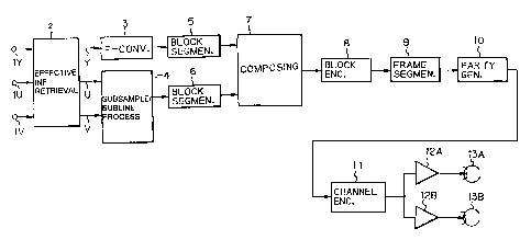
with reference to Fig. 1A . As shown therein, a digital
l0 luminance signal Y and digital color difference signals U and V,
which are formed by three primary color signals R, G and B, are
respectively supplied to input terminals 1Y, 1U and 1V. The
three primary color signals R, G, and B may, for example, be
supplied from a color video camera. The respective clock rates
of these signals are substantially the same as the frequencies of
the component signals of the above-mentioned D1 format digital
VTR. In other words, the sampling frequencies for the luminance
and color difference signals are 13.5 MHz and 6.75 MHz,
respectively. Similarly, the number of bits per sample is also 8
bits. Thus, the amount of data per second which is supplied to
the input terminals 1Y, 1U and 1V is also approximately 216 Mbps
as earlier described.
The signals from the input terminals 1Y, 1U arid 1V are
supplied to an effective information retrieval circuit 2 which
is adapted to omit or remove data from the received signals
DS6:2439.APP 12
205436
PATENT
39-0100.2439
during the blanking intervals and to retrieve information only
from the effective area. As a result, the data are compressed,
such that, the data rate is reduced to approximately 167 Mbps.
The luminance signal Y from the effective information
retrieval circuit 2 is supplied to a frequency conversion circuit
3. The frequency conversion circuit 3 converts the sampling
frequency from 13.5 MHz into a frequency which is 3/4 of 13.5
MHz. The frequency conversion circuit 3 may include a thin-out
filter so as to prevent reflected distortion from occurring. The
output signal of the frequency conversion circuit 3 is supplied
to a block segmentation circuit 5. The block segmentation
circuit 5 converts the received series luminance data into a
block sequence.
Fig. 3 is a schematic diagram illustrating a three-
dimensional arrangement of blocks which may be used by the block
segmentation circuit 5 as an encoding unit. More specifically,
by dividing a screen which may occupy, for example, two frames as
shown in Fig. 3, a large number of unit blocks (4 lines x 4
picture elements x 2 frames) are formed. In Fig. 3, the solid
lines represent lines associated with odd fields, while the
braken lines represent lines associated with even fields.
Returning to Fig. 1A, it will be seen that the two
color difference signals U and V from the effective information
retrieval circuit 2 are supplied to a subsampling and subline
processing circuit 4. The subsampling and subline processing
DS6:2439.APP 13
2054360
PATENT
39-0100.2439
circuit 4 converts the sampling frequency from 6.75 MHz into a
frequency which is 1/2 of 6.75 MHz and then alternately selects
one of the two digital color difference signals for each line.
Thereafter, the subsampling and subline processing circuit 4
composes the two digital color difference signals into one
channel of data and outputs a line sequential digital color
difference signal. Fig. 4 shows picture elements of a signal
which have been sub-sampled and sub-lined by the circuit 4. In
Fig. 4, "0" represents a sampling picture element of the first
color difference signal U; "d" represents a sampling picture .
element of the second color difference signal V; and "X"
represents a position in which a picture element has been thinned
out by the sampling processing.
The line sequential signal from the subsampling and
subline processing circuit 4 is supplied to a block segmentation
circuit 6. In a manner similar to the block segmentation circuit
5, the block segmentation circuit 6 converts scanning sequence
color difference data of television signals into a block sequence
data arrangement having a relatively large number of unit blocks,
in which each block may be (4 lines x 4 picture elements x 2
frames) in size. The output signals of the block segmentation
circuits 5 and 6 are supplied to a composing circuit 7.
The composing circuit 7 converts the received luminance
signal and the color difference signal which have been converted
into respective block sequence signals into one channel of data.
DS6:2439.APP 14
PATENT
39-0100.2439
The output signal of the composing circuit 7 is supplied to a
block encoding circuit 8. As will be more fully described
hereinafter, an encoding circuit adaptable to the dynamic range
(ADRC) of each block, a Discrete Cosine Transform (DCT) circuit,
or the like can be utilized in the block encoding circuit 8. The
output signal of the block encoding circuit 8 is supplied to a
frame segmentation circuit 9. The frame segmentation circuit 9
converts the received signal into data having a frame
construction. The frame segmentation circuit 9 exchanges between
a picture system clock and a record system clock.
The output signal of the frame segmentation circuit 9
is supplied to a parity generation circuit 10 which generates an
error correction code parity signal. The output signal of the
parity generation circuit 10 is supplied to a channel encoder 11
which performs channel encoding so as to decrease the low band of
the record data. The output signal of the channel encoder 11 is
supplied through recording amplifiers 12A and 12B and rotation
transformers (not shown) to magnetic heads 13A and 138,
respectively, and is then recorded on magnetic tape.
Referring now to Fig. lB,it will be seen that recording
side of the digital VTR there illustrated is similar to that of
Fig. 1A and, as such, only the differences therebetween will be
described below.
In Fig. 1B, a digital audio signal is supplied from an
input terminal 1A to an audio encoding circuit 15. The audio
DS6:2439.APP 15
2a54360
PATENT
39-0100.2439
encoding circuit 15 is adapted to compress the received audio
signal by differential pulse code modulation (DPCM) processing.
The output data of the audio encoding circuit 15 is supplied to
the frame segmentation circuit 9 which converts this output data,
along with the block encoded picture data from the block encoding
circuit 8, into data having a frame construction. The output
audio data supplied to the frame segmentation circuit 9 is real
time data and relates to the picture data.
The output signal of the frame segmentation circuit 9
in Fig. 1B is alsa supplied to a parity generation circuit 10
which generates an error correction code parity signal. The
output signal of the parity generation circuit 10 in Fig. 1B is
supplied to a mixing circuit 14. The output data of the audio
encoding circuit i5 is further supplied to a parity generation
circuit 16 which generates an error correction code parity
signal. The parity signal from parity generation circuit 16 is
supplied to the mixing circuit 14. Subdata from an input
terminal 1S is supplied to a parity generation circuit 17 which
performs an error correction encoding process on the received
subdata and generates a parity signal. The parity signal from
the parity generation circuit 17 is also supplied to the mixing
circuit 14.
The mixing circuit 14 is adapted to combine the
received parity signals from the parity generation circuits 10,
16 and 17 such that picture data, audio data and subdata are
DS6:2439.APP 16
20~43~0
PATENT
39-0100.2439
arranged in a predetermined pattern. The output signal of the
mixing circuit 14 is supplied to a channel encoder 11 which
performs channel encoding so as to decrease the low band of the
record data. The output signal of the channel encoder 11 is
supplied to a mixing circuit 18 along with a pilot signal for
automatic track following (ATF) control from an input terminal
19. The pilot signal is a relatively low frequency signal which
can be readily separated from the record data. The output signal
of the mixing circuit 18 is supplied through recording amplifiers
12A and 12B and rotation transformers (not shown) to magnetic
heads 13A and 13B, respectively, and is then recorded on magnetic
tape.
In the above-described signal process portion of the
recording sides of digital VTR shown on Figs. 1A and 1B, by not
considering the blanking intervals and by retrieving data only
from the effective area, the input data rate of 216 Mbps is
decreased to approximately 167 Mbps. The frequency conversion
and the sub-sample and sub-line processing further reduce the
data rate to approximately 84 Mbps. As a result of the
compressing and encoding by the block encoding circuit 8, the
data rate is still further reduced to approximately 25 Mbps.
Thereafter, by adding additional information such as a parity
signal and an audio signal to the resultant compressed data, the
recording data rate becomes approximately 31.5 Mbps.
DS6:2439.APP 17
~05~360
PATENT
39-0100.2439
The playback sides of digital VTRs according to the
invention will now be described with reference to Figs. 2A and
2B. As is to be appreciated, the playback sides of Figs. 2A and
2B correspond to the recording sides of Figs. 1A and 1B,
respectively.
In Fig. 2A, playback data obtained from the magnetic
heads 13A and 13B are supplied through rotation transformers (not
shown) and playback amplifiers 21A and 21B, respectively, to a
channel decoder 22. The channel decoder 22 is adapted to
demodulate the received channel encoded data. The output signal
of the channel decoder 22 is supplied to a time base compensation
(TBC) circuit 23 which removes time base fluctuating components
from the reproduced signal. The reproduced playback data from
the TBC circuit 23 is supplied to an error correction code (ECC)
circuit 24 which corrects and modifies errors by utilizing a
predetermined error correction code. The output signal of the
ECC circuit 24 is supplied to a frame disassembling circuit 25.
The frame disassembling circuit 25 separates each
component of the block encoded picture data and exchanges between
the recording system clock and the picture system clock. Each
data component separated i.n the frame disassembling circuit 25 is
supplied to a block decoding circuit 26, The block decoding
circuit 26 decodes the received data in accordance with the
original data of each block and supplies the decoded data to a
distribution circuit 27. The distribution circuit 27 separates a
DS6:2439.APP l8
~o~~~s
PATENT
39-0100.2439
luminance signal and color difference signal from the received
decoded data which are supplied to block disassembling circuit 28
and 29, respectively. The block disassembling circuits 28 and 29
function in a substantially opposite manner to that of block
segmentation circuits 5 and 6 of Fig. 1A. More specifically, the
block disassembling circuits 28 and 29 convert the received block
sequence signals into raster scanning sequence signals.
The decoded luminance signal from the block
disassembling circuit 28 is supplied to an interpolation filter
30 which converts the sampling rate of the luminance signal from
3 fs to 4 fs (4 fs = 13.5 MHz). The digital luminance signal Y
from the interpolation filter 30 is supplied to an output
terminal 33Y.
On the other hand, the digital color difference signal
from the block disassembling circuit 29 is supplied to a
distribution circuit 31. The distribution circuit 31 separates
digital color difference signals U and V from the line sequential
digital color difference signals U and V. The separated digital
color difference signals U and V are supplied from the
distribution circuit 31 to an interpolation circuit 32. The
interpolation circuit 32 interpolates the received decoded
picture element data to obtain the line and picture element data
which have been previously thinned out by the circuit 4 of Fig.
1A. The interpolation circuit 32 supplies digital color
D56:2439.APP 19
X054360
PATENT
39-0100.2439
difference signals U and V, each having a sampling rate of 4 fs,
to output terminals 33U and 33V, respectively.
The playback side of the digital VTR of Fig. 2B is
similar to that of Fig. 2A and, as such, only the differences
therebetween will be described below.
In Fig. 2B, playback data obtained from the magnetic
heads 13A and 13B are supplied through rotation transformers (not
shown) and playback amplifiers 21A and 21B, respectively, to the
channel decoder 22 and an ATF circuit 34. As previously
described, the channel decoder 22 is adapted to demodulate the ,
received channel encoded data. The output signal of the channel
decoder 22 is supplied to the TBC circuit 23 which removes time
base fluctuating components from the playback signal. The ATF
circuit 34 generates a tracking error signal in accordance with
the level of a beat component of the reproduced pilot signal.
The tracking error signal from ATF circuit 34 may be supplied to
a phase servo circuit of a capstan servo circuit (not shown).
The ATF circuit 34 functions in substantially the same manner as
that of a conventional VTR.
The playback data from the TBC circuit 23 is supplied
to ECC circuits 24, 37 and 39 which correct and modify errors by
using a predetermined error correction code. More particularly,
the ECC circuit 24 corrects and modifies errors in the picture
data, the ECC circuit 37 corrects and modifies errors in the
audio data recorded in an audio dedicated area, and the ECC
DS6:2439.RPP 20
205360
PATENT
39-0100.2439
circuit 39 corrects errors in the subdata. The output signal of
the ECC circuit 37 is supplied to an audio decoding circuit 38
which decodes the compressed and encoded audio signal. The
decoded data from the audio decoding circuit 38 are supplied to a
composing circuit 36. The subdata from the ECC circuit 39 is
supplied through an output terminal 33S of the ECC circuit 39 to
a system controller (not shown) which controls the operations of
the VTR. The output signal of the ECC circuit 24 is supplied to
a frame disassembling circuit 25.
The frame disassembling circuit 25 separates each
component of the block encoded picture data and exchanges between
the recording system clock and the picture system clock. Each
data component separated in the frame disassembling circuit 25 is
supplied to a block decoding circuit 26, as previously described.
The frame disassembling circuit 25 further separates audio data
from the received signal and supplies the separated audio data to
an audio decoding circuit 35. The audio decoding circuit 35
decodes the separated audio data so as to retrieve the original
audio data which are supplied to the composing circuit 36. The
composing circuit 36 switches between the two audio signals
received from the decoding circuits 35 and 38 or combines them in
a close fading arrangement and supplies the output audio signal
to an output terminal 33A.
The block encoding circuit 8 of Fig. 1A or 1B may
include an ADRC (Adaptive Dynamic Range Coding) encoder similar
DS6:2439.APP 21
204360
PATENT
39-0100.2439
to that disclosed in Japanese Patent Application Nos. SHO 59-
266407 and SHO 59-2698666, which have a common assignee herewith.
Such ADRC encoder generally detects the maximum value MAX and the
minimum value MIN of data representing a plurality of picture
elements contained in each block and then calculates a dynamic
range DR of the block from the detected maximum and minimum
values. Thereafter, the ADRC encoder encodes the data in
accordance with the dynamic range such that the data are
requantized so as to have a lesser number of bits than those of
the original picture element data.
Alternatively, the block encoding circuit 8 may include
a discrete cosine transform circuit in which the picture element
data of each block is subjected to discrete cosine transform
(DCT) processing and the coefficient data obtained by the DCT
processing are quantized. Thereafter, the quantized data are
compressed by utilizing the run-length Huffman encoding process.
An example of a block encoding circuit having an ADRC
encoder, in which-the picture quality is not degraded by multiple
dubbing operations, will now be described with reference to Fig.
5 in which an input terminal 41 receives the output signal from
the composing circuit 7 of Fig. 1A or 1B where each sample of the
signal has been quantized to 8 bits.
The block segmentation data from the input terminal 41
are supplied to a maximum value and minimum value detection
circuit 43 and a delay circuit 44. The maximum value and minimum
DS6:2439.APP 22
204360
PATENT
39-0100.2439
value detection circuit 43 detects the minimum value MIN and the
maximum value MAX for each block of received data. The delay
circuit 44 delays the received data for the time period necessary
for the circuit 43 to detect the maximum and minimum values. The
picture element data from the delay circuit 44 are supplied to
comparison circuits 45 and 46.
The maximum value MAX and the minimum value MIN from
the detection circuit 43 are supplied to a subtraction circuit 47
and an addition circuit 48, respectively. The value of a
quantized step width for the situation in which non-edge matching
quantization is performed with a fixed length of 4 bits, that is
D = 1/16 DR, is applied from a bit shift circuit 49 to the
subtraction circuit 47 and the addition circuit 48. More
specifically, in the bit shift circuit 49, the dynamic range DR
is shifted by 4 bits sa as to deviate or shift the dynamic range
by (1/16). The value D may be a fixed value which is equivalent
to a noise level value and the quantizing step width value. The
subtraction circuit 47 subtracts the quantized step width value D
from the maximum value MAX and outputs a threshold value of
(MAX - D). On the other hand, the addition circuit 48 adds the
quantized step width D value and the minimum value MIN together
and outputs a threshold value of (MIN + A). The threshold values
from the subtraction circuit 47 and the addition circuit 48 are
supplied to the comparison circuits 45 and 46, respectively.
DS6:2439.APP 23
204360
PATENT
39-0100.2439
The output signal of the comparison circuit 45 is
supplied to one input terminal of an AND gate 50. The output
signal of the comparison circuit 46 is supplied to one input
terminal of an AND gate 51. The delayed data from the delay
circuit 44 are supplied to the other input terminals of AND gates
50 and 51.
The output signal of the comparison circuit 45 is a
relatively high value when the level of the data from the delay
circuit 44 is greater than that of the threshold value. When
this occurs, picture element date from the delay circuit 44
having level values in the maximum level range of (MAX to MAX -
d) are supplied from the output terminal of AND gate 50. On the
other hand, the output signal of the comparison circuit 46 is a
relatively high value when the level of the data from the delay
circuit 44 is less than that of the threshold value. When this
occurs, picture element data from the delay circuit 44 having
level values in the minimum level range of (MIN to MIN + D) are
supplied from the output terminal of AND gate 51.
The output signals of AND gates 50 and 51 are
respectively supplied to averaging circuits 52 and 53 which
calculate average values for each block. A reset signal is
supplied from a terminal 54 to the averaging circuits 52 and 53
at a rate corresponding to the block intervals.' The averaging
circuit 52 outputs an average value MAX' of the picture element
data in the maximum level range of (MAX to MAX - D). Similarly,
DS6:2439.APP 24
~~~4~6~
PATENT
39-0100.2439
the averaging circuit 53 outputs an average value MIN' of the
picture element data in the minimum level range of (MIN to MIN +
D). The average values MAX' and MIN' are supplied to a
subtraction circuit 55 which subtracts the average value MIN'
from the average value MAX' and outputs an adjusted dynamic range
DR'.
The average value MIN' is further supplied to a
subtraction circuit 56. The delayed data from the delay circuit
44 is supplied through a delay circuit 57 to the subtraction
circuit 56. The subtraction circuit 56 subtracts the average
value MIN' from the delayed data from the delay circuit 57 and
outputs data PD1 in which the minimum value has been removed.
The data PD1 is supplied through a delay circuit 63 to a
quantizing circuit 58, which may include a ROM. The adjusted
dynamic range DR' from the subtraction circuit 55 and a bit
number n from a bit number determination circuit 59 are also
supplied to the quantizing circuit 58. More specifically, in the
embodiment being described, ADRC with variable length encoding is
used, with the number of bits assigned for quantization being one
of 0 bits (no code signal transmission), 1 bit, 2 bits, 3 bits or
4 bits, and with an edge matching quantizing operation being
performed. The bit number determination circuit 59 determines
the number of bits (n) to be assigned for each block and applies
corresponding data to the quantizing circuit 58.
DS6:2439.APP 2 5
205430
PATENT
39-0100.2439
In ADRC with variable length encoding, for a block
having a relatively small dynamic range DR', the bit number n is
decreased, while for a block having a relatively large dynamic
range DR', the bit number n is increased. Thus, the encoding
operation can be effectively performed.
To further clarify this matter, consider the situation
in which a threshold value for determining the bit number n is T1
to T4 (where T1 < T2 < T3 < T4). For a block in which (DR' <
T1), the dynamic range DR' information is transmitted, but not
l0 the code signal. For a block in which (T1 <= DR' < T2), (n = 1)
is assigned. For a block in which (T2 <= DR' < T3), (n = 2) is
assigned. For a block in which (T3 <= DR' < T4), (n = 3) is
assigned. For a block in which (DR' >= T4), (n = 4) is assigned.
In ADRC with variable length encoding, by varying the
threshold values T1 to T4, the amount of information generated or
supplied can be controlled, that is, the information can be
buffered. Thus, even for a transmission path as in the present
digital VTR in which the amount of supplied information is set to
a predetermined value, ADRC with variable length encoding can be
utilized:
Referring again to Fig. 5, a buffering circuit 60
receives the dynamic range DR' from the subtraction circuit 55
and is adapted for determining the threshold values T1 to T4 so
as to set the amount of information which may be generated or
supplied to a predetermined value. The buffering circuit 60 has
DS6:2439.APP 26
~o~~~so
PATENT
39°0100.2439
a plurality of sets, for example, 32 sets, of threshold values
(T1, T2, T3, T4). The sets of the threshold values are
identified by a parameter code Pi (where i = 0, 1, 2, ... , 31).
In a preferred embodiment, as the value of i increases, the
amount of information which may be generated linearly decreases.
However, as the amount of generated information decreases, the
quality of the picture being recorded is degraded.
The threshold values T1 to T4 from the buffering
circuit 60 are supplied to a comparison circuit 61. The.dynamic
range DR' from the subtraction circuit 55 is also supplied to the,
comparison circuit 61 through a delay circuit 62. The delay
circuit 62 delays the dynamic range DR' for the time period
necessary for the buffering circuit 60 to select a set of
threshold values. The comparison circuit 61 compares the dynamic
range DR' of the block with each threshold value and supplies a
compared output to the bit number determination circuit 59. As
previously described, the determination circuit 59 determines the
number of bits (n) to be assigned to the block and supplies data
representing such number to the quantizing circuit 58. The
quantizing circuit 58 converts the data PD1 received from the
delay circuit 63, in which the minimum value has been removed as
previously described, into a code signal DT by the edge matching
quantizing operation utilizing the received dynamic range DR' and
the assigned bit number n. This code signal DT is outputted from
the quantizing circuit 58.
DS6:2439.APP 2~
204360
PATENT
39-0100.2439
The dynamic range DR' and the average value MIN' from
the delay circuits 62 and 64, respectively, are outputted.
Furthermore, the parameter code Pi which represents the code
signal DT and the set of threshold values is outputted.
In the above-described arrangement, since a signal
which had been quantized in a non-edge matching operation is
requantized in an edge matching operation in accordance with
information concerning the dynamic range, the degradation of
pictures being dubbed is relatively minimal.
Practical arrangements of the channel encoder 11 (Fig.
1A or 1B) and the channel decoder 22 (Fig. 2A or 2B) may be as
disclosed in 3apanese Patent Application No. HEI 1-143,491,
having a common assignee herewith, and as now further described
with reference to Figs. 6 and 7, respectively.
More particularly, in the channel encoder 11 of Fig. 6,
the output of the parity generation circuit 10 is supplied to an
adaptive type scramble circuit 71. In fact, a plurality of M
system scramble circuits are provided, with one of such circuits
being selected so that the high frequency component and the DC
component are smallest therein with respect to the input signal.
The output of the scramble circuit 71 is supplied to a partial
response class 4 detection type precoder 72.
The precoder 72 calculates 1/1 - D2 (where D is a unit
delay or delay operator). The precoder output is supplied to the
magnetic heads 13A and 13B through the record amplifiers 12A and
DS6:2439.APP 2 8
2fl~4~6fl
PATENT
39-0100.2439
12B, respectively, for recording on the tape. The reproduced
signals output from the heads 13A and 13B are amplified by the
playback amplifiers 21A and 21B prior to being supplied to a
partial response class 4 calculation process circuit 73 in the
channel decoder 22 ( Fig. 7). The circuit 73 performs the
calculation 1 + D on the reproduced output signals and, the
result of such calculation, is supplied to a Viterbi decoding
circuit 74 which decodes the output of the calculation process
circuit 73 in accordance with the Viterbi algorithm.
As disclosed in "Analog Viterbi Decoding far High Speed
Digital Satellite Channels", A.S. Acampora et al., IEEE
Transactions on Communications, Vol. Com. 26, No. 10, October
1978, pages 1463-1470; and in "The Viterbi Algorithm", G.D.
Forney, fir., Proceedings of the IEEE, Vol. 61, No. 3, March 1973,
pages 268-278, the Viterbi decoding circuit 74 utilizes
likelihood of correlation between data input successively thereto
for detecting transit of the data and decodes the data on the
basis of the detected result. Since the relationship (1-D2) of
the reproduced signal relative to the signal used for recording
(hereinafter referred to as the "recording signal") is utilized
to decode the recording signal from the reproduced signal and
then the digital video signal is decoded by the circuit 74 on the
basis of the decoded data, the bit error rate of the decoded data
can be reduced as compared with a standard decoding circuit which
decodes data with reference to the signal level. Therefore, the
DS6:2439,APP 29
~0~4360
PATENT
39-0100.2439
decoded data output by the Viterbi decoding circuit 74 has high
noise resistance. More specifically, by reason of the Viterbi
decoding circuit 74 in the channel decoder 22, the reproduced C/N
(carrier/noise) ratio is improved by 3 dB in respect to that
achieved when decoding bit-by-bit.
As shown in Fig. 8A, the magnetic heads 13A and 13B may
be mounted in diametrically opposed positions on a rotation drum
76. However, as shown in Fig. 8B, the magnetic heads 13A and 13B
are desirably mounted on the drum 76 adjacent each other in a
unified construction. A magnetic tape (not shown on either Fig.
8A or 8B) is wrapped obliquely on the peripheral surface of the
drum 76 with a winding angle of approximately 180°. With the
head locations shown in Fig. 8A, the magnetic heads 13A and 13B
are alternately contacted with the magnetic tape. On the other
hand, with the heads located as shown in Fig. 8B, both of the
magnetic heads i3A and 13B scan the magnetic tape at the same
time.
The directions of the gaps of the magnetic heads 13A
and 13B differ from each other, that is, the heads 13A and 13B
have different azimuth angles. For example, as shown in Fig. 9,
azimuth angles of ~ 20° are given to the magnetic heads 13A and
13B, respectively. By reason of the difference of the azimuth
angles, a record pattern is formed on the magnetic tape, as shown
in Fig. 10, in which adjacent tracks TA and TB on the magnetic
tape are formed by the respective magnetic heads 13A and 13B,
DS6:2439.APP 3 0
2054360
PATENT
39-0100.2439
which have different azimuth angles. Thus, when the magnetic
tape is played back or reproduced, due to an azimuth loss or
attenuation, the amount of cross talk between adjacent tracks can
be decreased.
Figs. 11A and 11B show a practical arrangement in which
the magnetic heads 13A and 13B are adjacent each other, as in
Fig. 8B and included in a unified structure to provide a so-
called double azimuth head. By way of example, the unified
magnetic heads 13A and 13B are shown to be mounted on an upper
drum 76 which is rotated at a high speed of 150 rps for the NTSC ,
system, while a lower drum 77 is fixed. Therefore, the unified
heads 13A and 13B effect 2 1/2 revolutions with the upper drum 76
for each NTSC field so that each field is recorded in five
tracks. In other words, each field is divided into five segments
recorded in respective tracks on the magnetic tape. By using
this segment system, the length of the tracks can be decreased
and, as a result, the track linearity error can be decreased.
For example, the winding angle D of the magnetic tape 78 on the
drum assembly 76-77 is desirably set to be less than 180°, for
example, approximately 166° and the drum diameter ~ is desirably
determined to be less than 25 mm, for example, 16.5 mm.
When recording on relatively narrow tracks, for
example, tracks having a pitch of approximately 5.5 Vim,
mechanical errors in the head and drum system may affect the
mechanical interchangeability. These mechanical errors may
DS6:2439.APP 3 1
2o543so
PATENT
39-0100.2439
include static track linearity error, dynamic tracking linearity
error and error in the positioning or pairing of the heads 13A
and 13E.
The static track linearity error may be caused by
nonlinearity of a lead on the drum, misalignment of the tape path
and inclination of the rotational axis of the drum. The
nonlinearity of the drum lead and the misalignment of the tape
path are related to the track length, and the inclination of the
rotational axis of the drum is related to the drum diameter.
More specifically, the tracking factor, which is an indication of ,
the static track linearity, is proportional to the track pitch
and inversely proportion to the product,of the track length and
the drum diameter. In the above-described arrangement, the drum
diameter is reduced from 40 mm to 16.5 mm and the track length is
reduced from approximately 74 mm to approximately 26 mm, as
compared with the drum diameter and track length, respectively,
of a conventional 8 mm analog VTR. Therefore, a tracking factor
larger than that of the 8 mm analog VTR can be obtained even
through the track pitch is relatively small, for example, 5.5 ~,m.
Thus, the static track linearity error for a digital VTR
embodying this invention is less than that of the conventional
8 mm VTR.
By using the double azimuth head, simultaneous
recording is performed. Normally, due to eccentricity or the
like of the rotating upper drum 76 relative to the fixed lower
DS6:2439.APP 32
205430
PATENT
39-0100.2439
drum 77, the magnetic tape 78 vibrates and thereby a track
linearity error takes place. As shown in Figs. 12A and 12B, if
the heads are diametrically opposed, the eccentricity of the
rotary upper drum 76 may urge the tape 78 downwardly when one of
the heads, for example, the head 13A, traces a track on the tape
(Fig. 12A), whereas, the tape 78 is urged upwardly when the other
head 13B traces a track on the tape (Fig. 12B). By reason of the
foregoing, adjacent tracks will be oppositely bowed and track
linearity is substantially degraded. On the other hand, when the
magnetic heads 13A and 13B are unified so as to substantially
simultaneously scan respective tracks on the tape, any
eccentricity of the rotary upper drum 76 similarly influences the
linearity of the tracks scanned by both heads so that the
linearity error is relatively reduced. Moreover, the distance
between the heads 13A and 13B is relatively small when the heads
are unified, as in the so-called double azimuth head, so that the
paired heads can be more accurately adjusted then when the heads
are diametrically opposed.
The above-described tape and head system enables tracks
having a relatively narrow width or pitch, such as no more than
5.5 Vim, to be recorded on the magnetic tape 78. Errors which may
be produced by using this tape and head system are typically lass
than that produced by the conventional 8mm VTR.
The tape used in the magnetic recording apparatus
embodying this invention is desirably produced as described below
DS6:2439.APP 33
2054360
PATENT
39-0100.2439
so as to contribute to the attainment of the desired high
recording density:
A solution containing an emulsion whose principal
component is an acrylic acid latex is coated on a base film
composed of a 7 ~m thick polyethylene phthalate (PET).
Thereafter, the base material is dried and thereby only fine
projections made of the emulsion particles are formed. As a
result, the surface roughness of the base material, measured as
the center line average height, Ra, is about 0.0015 ~m and the
to density of the fine projections is approximately 5,000,000 ,
particles / mm2.
Thereafter, by using a vacuum deposition unit shown in
Fig. 13, a magnetic layer whose principal component is cobalt
(Co) is formed on the base material in an oxygen atmosphere by
the so-called slant-deposition method.
More particularly, the vacuum deposition unit of Fig.
13 is shown to include two communicating vacuum chambers 81a and
81b with a partition 82 therebetween, and with a vacuum exhaust
valve 83 connected with the chamber 81b and through which both
chambers 81a and 81b can be evacuated. A supply roll 84 of the
base material B for the magnetic tape is rotatably mounted within
the chamber 81a, and a take-up roll 85 on which the completed
magnetic tape material is wound is rotatably mounted within the
chamber 81b. A guide roller 86 is situated in an opening in the
partition 82 approximately at the same level as the rolls 84 and
DS6:2439.APP 34
2054360
PATENT
39-0100.2439
85, and cylindrical cooling cans 87a and 87b are rotatably
mounted within the chambers 81a and 81b, respectively, at levels
substantially below that of the guide roller 86 so that the base
material B being unwound from the supply roll 84 is led
downwardly therefrom under the cooling can 87a, then over the
guide roller 86 and under the cooling can 87b prior to being
rewound on the take-up roll 85. Evaporation sources of cobalt
88a and 88b which, for example, may be ingots of 100% cobalt, are
provided in the chambers 81a and 81b, respectively, and are
heated by electron beams indicated~schematically at 89a and 89b.
Insulating shields 90a and 90b extend below the cooling cans 87a
and 87b, respectively, for restricting the incident angles at
which cobalt evaporated from the sources 88a and 88b can impinge
on the base material B running under the cooling cans 87a and
25 87b. Finally, the chambers 81a and 81b are provided with oxygen
gas supply pipes 91a and 91b for directing flows of oxygen
against the surface of the base material B at areas thereof where
evaporated cobalt is being deposited on the base material.
In the above-.described vacuum deposition unit, as the
web of base material B travels therethrough from the supply roll
84 past the cooling can 87a, the guide roller 86 and the cooling
can 87b to the take-up roll 85, two cobalt (Co) layers forming a
magnetic coating are deposited at an angle to the base material,
that is, by the slant deposition method, in an oxygen atmosphere.
DS6:2439.APP 35
w 254360
PATENT
39-0100.2439
The conditions under which such vacuum deposition is
effected, are as follows:
The vacuum chambers 81a and 81b are maintained at a
vacuum of 1 x 10⁻⁴ Torr., while the pipes 91a and 91b introduce
oxygen at a rate of 250 cc/min. into the vacuum chambers. The
shields 90a and 90b are arranged so that the incident angles of
the evaporated cobalt relative to the base material B are between
45° and 90°. The cobalt layer deposited on the base material at
each of the cooling cans 87a and 87b is provided with a thickness
of 1000 angstrom units, so that the total thickness of the
magnetic layer formed on the base material is 2000 angstrom
units.
After the magnetic layer composed of two cobalt layers
has been formed on the web of base material B, the back or under
side of the base material is coated with a uniform mixture of
carbon and epoxy resin binder, and the cobalt magnetic layer is
top coated with a perfluoro-polyether, as a lubricant. Finally,
the coated web of base material B is cut into strips having
widths of 8mm so as to produce the desired magnetic tapes.
The magnetic tape produced as described above, has been
found to have the following characteristics:
a residual magnetic flux density (Br) of 4,150 G;
a coercive force He of about 1690 Oe;
a rectangular ratio Rs of 790;
DS6:2439.APP 3 6
2~543~~
PATENT
39-0100.2439
and a surface roughness with a center line average
height Ra as small as 0.0015 Vim, which is due to the very low
surface roughness of the base material B.
Although surface roughnesses are usually measured in
accordance with JIS B 0601, the above noted surface roughness was
measured under the following conditions:
measuring instrument: Talystep (from Rank/Taylor, Inc.)
stylus diameter: 0.2 x 0.2 ~m (rectangular stylus)
stylus pressure: 2 mg
high-pass filter: 0.33 Hz.
Referring now to Fig. 14, it will be seen that a
magnetic head desirably used in a magnetic recording apparatus
embodying the present invention has monocrystal Mn-Zn ferrite
cores lOlA and 101B on which Fe-Ga-Si-Ru soft magnetic layers 102
and 103 are formed, by sputtering, for forming a gap 104
therebetween. Both sides of the gap 104, in the direction of the
track width, are filled with glass, as at 105 and 106, to limit
the effective gap length to 0.20 Vim, and to limit the track width
to approximately 4~m. A winding hole 107 is provided for
receiving a recording coil (not shown).
Since the magnetic head of Fig. 14 provides the Fe-Ga-
Si-Ru soft magnetic layers 102 and 103 having a saturation
magnetic flux density Bs of 14.5 kG in the vicinity of the gap
104, it is possible for the magnetic head to record data on a
DS6:2439.APP 37
~0~4360
PATENT
39-0100.2439
magnetic tape of high coercive force without causing magnetic
saturation of the head.
By using the (ME) metal evaporated tape and the
magnetic head as described above, a recorded bit area of 1.25
~m2/bit or less can be achieved, so as to obtain an areal
recording density of 0.8 bits/~m2. In other words, the described
ME tape and magnetic head make it possible to record a signal
with the shortest wavelength of 0.5~m on a track having a width
of 5~m so that the bit area of 1.25~m2/bit can be achieved while
minimizing the deterioration of the C/N ratio of the reproduced
output that otherwise results as the recording wavelength and
track width are reduced.
In 1988, the assignee of this application produced an
experimental consumer digital VTR which incorporated an ADRC bit
reduction scheme, scrambled NRZ coding, a class IV partial
response (PR4) detection scheme, and a modified 8mm video
transport mechanism used with ME tape. With a rotary drum having
a diameter of 40mm and a rotation speed of 60 rps, and using a
track pitch of 15 ~m at the wavelength of 0.5 Vim, a raw bit error
rate of 4 x l0-5 and a C/N of 51 dB (with a resolution bandwidth
of 30 KHz) at the half-Nyquist frequency were obtained. When
such experimental consumer digital VTR was used with a track
width of 5 Vim, the C/N obtained was only approximately 44 dB and
the picture quality was correspondingly degraded. However, the
various features described above in respect to the apparatus for
DS6:2439.APP 38
2~~4360
PATENT
39-0100.2439
magnetically recording digital data in accordance with this
invention, and in respect to the ME tape for use therewith, serve
to compensate for the reduction of the C/N by 7 dB, that is, make
it possible to obtain a C/N of 51 dB with a track pitch of 5 um.
In connection with the foregoing, it is known that an
increase in the space between the tape and the magnetic head
recording or reproducing a signal on the tape causes the signal
output level to decrease. Further, it is known that the space
between the tape and the magnetic head depends on the flatness of
20 the tape. In the case of a tape of the coated-type, the flatness
of the tape depends on the coating material that is used,
whereas, in the case of a vacuum deposited tape, such as, an ME
tape, the flatness of the tape surface depends on the smoothness
of the base material on which the metal is vacuum deposited. It
has been determined that, when the surface of the base film is
made as flat as possible, for example, as described above the C/N
is increased by 1 dB. Furthermore, by effecting the vacuum
deposition of cobalt on such base material or film in the manner
described above, with reference to Fig. 13, the C/N ratio is
further improved by 3 dB, as compared with the tape used in the
experimental consumer digital VTR produced in 1988. Further, by
using a Viterbi channel decoding scheme, as described above,
there is realized a further increase of 3 dB in the C/N ratio
over the bit-by-bit decoding scheme employed in the experimental
apparatus.
DS6:2439.APP 3g
2054360
PATENT
39-0100.2439
As a result, the deterioration of 7 dB in the C/N ratio
associated with a reduction of the track pitch to 5 ~m is fully
compensated so that, with a recording density resulting in a bit
area of 1.25 um2/bit, the described embodiment of this invention
makes it possible to achieve a raw bit error rate of 4 x 10⁻⁵,
that is, a raw bit error rate equivalent to that achieved by the
experimental apparatus of 1988 with a track pitch of 15 Vim. In
connection with the foregoing, it is to be noted that the raw bit
error rate, that is, the bit error rate prior to correction,
needs to be 10-4 or less in order to ensure that the errors will -
be contained within a correctable amount when error correction
codes with a redundancy of about 20% are employed.
Therefore, a digital picture signal can be recorded on
a magnetic tape with a relatively high density by using tracks
having a relatively small pitch in accordance with the described
embodiment of the present invention. As a result, such
embodiment of the present invention enables a relatively long
recording or reproducing operation to be performed on a magnetic
tape that can be contained in a relatively small size cassette.
Furthermore, since a relatively small diameter rotational drum is
utilized, the size of the cassette housing and of the tape
loading mechanism can be further reduced for minimizing the size
of the VTR.
DS6:2439.APP 40
_\
~p~4~~0
PATENT
39-0100.2439
An example of a tape cassette 211 for use with the
above-described recording and reproducing apparatus will now be
described with reference to Figs. 15A, B, C and D.
As shown in Fig. 15 A, a transparent window 215 is
provided on the top wall of the tape cassette 211 to enable a
visual inspection of the inside of the tape cassette. The
dimensions of the tape cassette 211 axe slightly smaller than
those of the cassette intended for use in the conventional 8 mm
analog VTR. As shown in Figs. 15A and B, the dimensions of the
tape cassette 211 may be 93 mm (width) x 69 mm (depth) x 12 mm
(thickness). Fig. 15C illustrates the tape cassette 211 with its
top wall removed to show hubs 213 and 214 which are rotatably
disposed within the tape cassette housing. The magnetic tape 78
is wound around hubs 213 and 214, and is suitably guided
therebetween.
As shown in Figs. 15 A and D, a pivoted cover or lid
212 is mounted at the front of the tape cassette 211. When the
tape cassette 211 is loaded into a VTR (not shown), the lid 212
is pivotally opened by a conventional member provided therefor
within the VTR, so as to allow access to the magnetic tape 78
contained in the cassette housing.
The tape cassette 211 having the indicated dimensions
is, nevertheless, adapted to contain an amount of the magnetic
tape 78 sufficient to enable 4 hours of recording operations.
The number of bits to be recorded in 4 hours is:
DS6:2439.APP 4 1
204360
PATENT
39°0100.2439
31.56 x 106 x 60 x 60 x 4 = 4.545 x 1011 bits
The required tape area needed to record 4.545 x 10110
bits of data is:
4.545 x 1011 x 1.25 (~.m2~bit) = 5,681 x 105 mm2
If, for example, the tape has a width of 6 mm and an
effective width of 5 mm, the length of tape needed to obtain a
tape recording area of 5.681/ x 105 mm2 is:
5.681 x 105 mm2 / 5 mm = 113,625 mm = 113.6 m
The volume occupied by a tape having a length of 113.6
1~0 m, width of 6 mm and a thickness of 7 ~,m is:
113.6 x 103 x 6 x 0.007 = 4771.2 mm3
The radius x of a reel containing a tape having a
length of 113.6 and a width of 6 mm (assume that the diameters of
the reel hubs 213 and 214 are each 16 mm) can be derived, as
follows:
x2 ~r x 6 = 82 ~ x 6 + 4771.2
x = 17.8 mm.
Since the maximum allowable winding radius of the tape
78 in the tape cassette 211 is 22 mm, as shown in Fig. 15C, the
above-described amount of tape can be well contained on reel hubs
213 and 214 in the tape cassette 111. Thus, a recording
operation of 4 hours can be performed.
Although the above calculations have assumed a tape
width of 6 mm and an effective width, that is, the width of the
tape across which signals can be recorded, of 5 mm, it is to be
DS6:2439.APP 42
2054360
PATENT
39-0100.2439
understood that, in accordance with this invention, the tape
width may be as large as 8 mm (effective width 7 mm) or as small
as 5 mm (effective width 4 mm) with the limits of the recording
time being correspondingly adjusted.
A tape loading mechanism for use with the above-
described recording and reproducing apparatus will now be
described with reference to Fig. 16 which shows a drum chassis
111 and a cassette support chassis 114. The drum chassis 114 has
a drum 76, a tension regulator 112 and a capstan 113 mounted
thereon. On the other hand, the cassette support chassis 114
operatively positions a cassette 115 which contains, reels 116
and 117 and roller guides 118, 119, 122 and 123 for the tape 78
running between the reels.
In an unloaded state, that is, when the tape 78 in the
cassette 115 on chassis 114 is not loaded so as to engage the
drum 76 on chassis 111 of a VTR, the drum chassis 111 is in the
position shown by the broken lines of Fig. 16. However, when the
tape 78 is to be loaded, a loading motor (not shown) is energized
to drive a gear 120 so as to move the drum chassis 111 toward the
cassette support 114. At the initiation of such movement of the
drum chassis 111, a lid of the cassette 115 (similar to the lid
212 on Fig. 15D) is opened so as to allow the drum 76, tension
regulator 112 and capstan 113 on chassis 111 to be inserted into
the cassette 115. More specifically, the drum 76 is inserted
into the cassette 115 so that the magnetic tape 78 between the
DS6:2439.APP 43
205~36~
PATENT
39-0100.2439
guides 122 and 123 is wound on a portion of the periphery of the
drum. This portion, or winding angle is less than 180°. In a
preferred embodiment, the winding angle is approximately 166°.
Further, the tension regulator 112 is inserted into a cut-out
portion at the front of the cassette 115 so as to contact the
magnetic tape 78 between the guides 11$ and 122 and impose a
predetermined tension thereon. Furthermore, the capstan 113 is
inserted so as to engage the tape between guides 119 and 123 with
a pinch roller 121 of the cassette 115, thereby causing the
magnetic tape 78 to travel about the drum 76 at a predetermined ,
rate.
Since the winding angle is relatively small, the
frictional drag of the moving magnetic tape on the drum 76 is
less than that of arrangements utilizing a larger winding angle.
This reduction in frictional drag is particularly advantageous
when the VTR is operated in a fast forward state or a rewind
state. Further, if the winding angle is 180° or more, cross talk
between signals may occur when two channels of data are recorded
or reproduced using a double azimuth head. However, using a
winding angle of less than 180°, as in the preferred embodiment
of the present invention, eliminates cross talk between signals.
Furthermore, since only one of the drum chassis 111 and the
cassette support chassis 114 is movable relative to the other,
the complexity of the loading mechanism can be minimized.
DS6:2439.APP 44
2054360
PATENT
39-0100.2439
As previously stated, one way to increase the recording
density is to decrease the track pitch. However, decreasing the
track pitch typically results in increased cross talk between
signals recorded in adjacent tracks. In the prior art, blank
spaces or guard bands are sometimes used between adjacent tracks
so as to isolate the signals recorded in those tracks, thereby
reducing cross talk. However, since signals are not recorded in
the guard bands, using them reduces the tape recording density.
Therefore, as is to be appreciated, it is desirable to eliminate
guard bands and yet still provide isolation between signals
recorded in adjacent tracks. One means to accomplish this for
high frequency signals is to position the heads which record in
adjacent tracks sa that the gaps of such heads have different
azimuth angles. More specifically, by providing the heads with
different azimuth angles, each head will strongly reproduce the
high frequency signals in the tracks corresponding to the
respective head., while the high frequency signals in the adjacent
tracks will not be substantially reproduced due to azimuth error
or attenuator. Heretofore, the azimuth angles have been about
10° or less.
However, in order to allow the track pitch to be
decreased to be about 5 um so as to increase the recording
density and still avoid cross talk between signals recorded in
adjacent tracks, the magnetic heads 13A and 13B are provided with
azimuth angles of ~ 20°, respectively.
DS6:2439.APP 45
20~436~
PATENT
39-0100.2439
The selection of the ~ 20° azimuth angles will now be
explained with reference to Fig. 17 which illustrates the
relationship between cross talk and azimuth angle. The values of
Fig. 17 were obtained from a reproduced signal passed through a
partial response class IV (PR 4) filter at the Nyquist frequency
for a case where the track pitch is approximately 5.5 ~m and the
speed of the magnetic tape 78 is approximately 7.75 m/sec. As
shown in Fig. 17, the amount of cross talk decreases as the
azimuth angle increases. However, as the azimuth angle increases
the effective relative speed in a direction normal to the gaps of ,
the magnetic heads 13A and 13B decreases. As a result, the level
of the playback signal decreases as shown, for example, in Fig.
18.
The following table shows the amount of decrease of the
cross talk and the amount of decrease of the playback signal
level when the azimuth angle is changed from 10° to various other
angles:
Azimuth angle Amount of decrease Amount of decrease
of cross talk (dB) of playback signal
(d8)
10 to 15 - 3.64 - 0.17
10 to 20 - 6.30 - 0.41
10 to 25 - 8.45 - 0,72
10 to 30 -10.31 - 1.12
DS6:2439.APP 4 6
~o~~~~o
PATENT
39-0100.2439
Tt has been found that, when the azimuth angle is
approximately 20°, both the amount of decrease of cross talk and
the amount of decrease of the playback signal are suitable for a
digital VTR.
Thus, in a preferred embodiment of the present
invention, the azimuth angles of the magnetic heads 13A and 13B
are set to approximately ~ 20°. There azimuth angles
significantly reduce the amount of cross talk between adjacent
tracks while ensuring that the level of the playback signal will
be at an acceptable level for digital signals. Therefore, by ,
using the azimuth angles of ~ 20°, tracks can be formed on the
magnetic tape 78 having a relatively narrow track pitch without
guard bands so as to increase the recording density.
Having described illustrative embodiments of the
invention with reference to the accompanying drawings, it is to
be understood that the invention is not limited thereto, and that
various changes and modifications can be effected therein by one
skilled in the art without departing from the scope or spirit of
the invention as defined in the appended claims.
DS6:2439.APP 47