Note: Descriptions are shown in the official language in which they were submitted.
2 ~ ~ ~ 3 ~
The present invention relates to control
circuits for pump motors. More specifically, the
field of the invention is that of liquid level
control circuits which automatically maintain the
liquid level within a predetermined range.
In sump and water tanks, for example, the
liquid level should be maintained within a ~ `
predetermined range for proper functioning of the ~ ~-
tank. Many prior art devices automatically
control the liquid level within the tank by -~ ~
activating a pump when the liquid rises above a ~ ;
first predetermined level and deactivating the
pump when the liquid level falls below a second
predetermined level. Some of the prior art
devices use mechanical or moving parts such as
mechanical switches op~rated by rubber diaphragms,
springs, rods, floats, or balls, all of which may -
j tend to wear out or mal~unction over time.
Other prior art devices use electrical or -`
optical probes positioned within the tank to
determine the liquid level and control the pump
accordingly. For example, self-heating ~ -; ;
thermistors or conductivity probes may be used.
However, such prior art systems using probes may `
be sensitive to humidity, moisture, changing - -
temperatures, and varying voltage levels in the
sensing circuit, all of which may produce
erroneous results and subject the probes to wear.
Also, contamination of the probes may adversely
effect their performance. The probes and their
associated circuitry may be adjusted to improve
performance, but making the adjustments may be
inconvenient and expensive. ~
~ .
:: -: `
;~x: ::
,~ 2~3~
! What is needed i5 a liquid level control -- -
~ which reliably operates without the need for
¦ adjustment.
Also needed is a liquid level control which
minimizes operating problems associat~.d with , ~
contamination and mechanical wear. '~ ~;
A further need exists ~or a liquid level
control which minimizes inaccuracies associated
with varying temperatures.
The present invention is a ~iquid level
control system utilizing capacitive sensors which -
avoids the aforementioned problems. Activating ;
circuitry starts the pump motor when both upper
and lower sensors indicate the presence of liquid.
The pump motor continues operation until both of
the capacitive sensors indicate the absence of
liquid, in which case the pump is shut off. The
circuitry of the present invention operates
reliably over a wide range of operating
conditions.
One construction of a capacitive sensor
includes having one electrode as a metal plate
disposed in a plastic box enclosing the circuitry/ :
and the other electrode as the pump case. This
provides a simple and reliable capacitive sensor
which is generally isolated from any problems of
contamination or mechanical failure.
Alternatively, a capacitive sensor may include an
insulated wire capable of mounting at any position ~- `
in the tank.
One portion of the circuitry includes
thermistors which can turn off the pump motor when
a predetermined temperature is reached. This is
; particularly important when the system is operated
~ 35 in a circulating mode wherein the liquid pumped
. ~.,"
~'' '' '~' '
2~38~
~; out of the tank is returned to the tank and the
;~ water temperature becomes increasingly higher.
Another portion of the circuitry maintains ; ---
voltages at switch terminals at predetermined ~i -
levels so that false triggering of the activating
circuitry does not occur, which can be
particularly troublesome at high operating
temperatures.
The present invention is, in one form, an -
apparatus for controlling liquid levels comprising i`
a pump, a motor drivingly connecked to the pump,
first and second sensors, and an activation
circuitry. The first sensor detects the presence ; -~
of liquid and at a first position, producing a
first signal indicative of the presence of liquid ~ ~-
at that first position. The second sensor detects -~
the presence of liquid and at a second position, ~ -~
producing a second signal indicative of the ~
presence of liquid at the second posi~ion. An ` :
activating device is operably coupled to the first
and second sensors, and starts the motor to drive ;
the pump when both of the first and second signals ;
are produced. The activating devices continues
operation of the motor while at least one of the -
first and second signals are being produced.
Finally, the activating device stops the motor
when both the first and second signals are no
longer produced. The first and second sensors
each include a capacitive circuit having two
capacitive electrodes.
The above mentioned and other features and
objects of this invention, and the manner of
attaining them, will become more apparent and the ~`
invention itself will be better understood by
reference to the following description of an
-~
embodiment of the invention taken in conjunction
with the accompanying drawings, wherein~
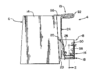
Figure 1 is a side, elevational view, in
partial cut-away, o~ the liquid contr~l system o~ -
the present invention. ~ ;-
Figure 2 is an enlarged cross-sectional view -~
taken along view lines 2-2 of Figure lo
.: .........
Figure 3 is a schematic circuit diagram of - ~ i
the control circuitry of the present invantion.
lo Corresponding reference characters indicate -
corresponding parts throughout the several views.
The exemplification set out herein illustrates one ;~
preferred embodiment of the invention, in one
form, and such exemplifications are not to be
construed as limiting the scope of the invention ~ -~
in any manner. - -~
The present invention comprises a liquid
level control system adapted for use in a tank or - - -- P
other vessel in which the level of liquid is to be
controlled. As depicted in Figure 1, control
system 4 includes pump 6, which can be a
submersible sump pump, controller box 8, and upper
sensor 10. The water in which control system 4 is
immersed acts as a conductive medium. Pump 6 is
disposed within the tank (not shown) in which the
liquid level is to be controlled, and includes
insulated motor 12 (see Figure 3) located within
pump casing 14. Controller box 8 is also disposed
within the tank, and is preferably attached to
casing 14. Circuit board assembly 16 and lower
sensor 18 are disposed within box 8. Box 8 is
spaced away from pump casing 14 by mounting posts
20, and preferably box 8 is made of a dialectric
material. Upper sensor 10 includes sensor portion
22 of insulated wire 24 which is vertically `~
adjustable at an upper portion o~ pump casing 14
i;'; ~ ' '
by means of mounting bracket 26. Sensor portion - -
22 is electrically coupled to circuit board 16 via
connecting portion 28 o~ insulated wire 24. ~-
Figure 2 shows the arrangement of lower
sensor 18. Metal plate 30 is located on bottom
wall 32 of box 8 and is separated fra,m any liquid
adjacent bottom wall 32 by the dielectric barrier
formed by the material of box 8, which i6
preferably plastic or the like. Printed circuit
board assembly 16 is secured vertically above
plate 30 and is connected to metal plate 30 by ~`
electrical wire 34. Epoxy potting compound exists
between circuit board assembly 16 and metal plate
30 so that assembly 16 and plate 30 are
electrically isolated.
Figure 3 shows the circuitry of the present
invention, most of which is generally located on
circuit board assembly 16. Alternating current
(AC) power supply 36 is selectively electrically
coupled to pump motor 12 by triac 38. Direct
current (DC) power supply 40 converts alternating
current from power supply 40 to a direct current
bus between DC positive terminal 42 and DC
negative terminal 44. Activating circuitry, ;
re~erred to generally by numeral 4S, is connected
to the direct current bus and selectively
activates triac 38 according to the states of ;~
upper and lower capacitive sensors C2 and C3 as ;~
described in more detail below. Grounding wire 48 ;~
;~ 30 is connected to pump case 14 to provide a ground
for the AC circuit through pump motor 12. A more
'~ detailed description of the circuitry of the ,~
present invention is provided below by describing
~ the arrangement and operation of activating ~ -
j 35 circuitry 46.
~` 6
Also shown in Figure 3, activating circuitry
, :-- . .-
:~i. 46 includes astable multivibrator 50 and
~;. monostable multivibrators 52 and 54. Astable
.~ multivibrator 50 includes NAND gate Gl, resistor - ~-
Rl, and capacitor Cl. NAND gate Gl has input pin
1 coupled to DC positive terminal 44, input pin 2 .
coupled to one terminal of resistor R1 and one
terminal of capacitor Cl, and output pin 3 coupled ~ ,
, to the cathode of diode D3, the cathode of diode ~-
D5, and the other terminal of resistor Rlo The
other terminal of capacitor Cl is coupled to DC `~
negative terminal 44.
~' Monostable multivibrator 52 includes NAND
J' gate G4, resistor R2, and upper sensor capacitor
C2. NAND gate G4 has input pin 12 coupled to DC
positive terminal 44 and one terminal of resistor
R2, input pin 13 coupled to the other terminal of
resistor R2, the anode of diode ~3, and the series
circuit of capacitors C2 and C4, and output pin 11
coupled to the base of transistor Q2. The series
circuit of capacitors C2 and C4 includes one
terminal of capacitor C4 coupled to input pin 13
of NAND gate G4, the other terminal of capacitor `~
C4 coupled to one terminal of capacitor C2, and
the other terminal of capacitor C2 coupled to DC
negative terminal 42.
Monostable multivibrator 54 includes NAND
gate G2, resistor R3, and lower sensor capacitor ;~
C3. NAND gate G2 has input pin 6 coupled to DC -~
positive terminal 44 and one terminal of resistor
R3, input pin 5 coupled to the other terminal of ::~
resistor R3, the anode of diode D4, and the series
circuit of capacitors C3 and C5, and output pin 4
coupled to the cathode of diode D4. The series
circuit of capacitors C3 and C5 includes one .
terminal of capacitor C5 coupled to input pin 5 of
`'``''':
NAND gate G2, the other kerminal of capacitor C5 -
coupled to one terminal of capacitQr C3, and the
.` other terminal of capacitor C3 coupled to DC
negative terminal 42. ~: ;
capacitors C4 and c5 are not needed to .
.. ~ achieve the desired functionality of monostable
multivibrators 52 and 54. As a precautionary
.i measure, however, capacitors C4 and C5 are
~-!'' included in activating circuitry 46 to limit the
~^.; 10 amount of current which could potentially pass ~;
through the liqjuid in case that insulation on any
,. of the sensor wires is damaged.
NAND gate G3 is coupled to monostable
! multivibrator 54 via diode D4, wherein the anode -
of diode D4 is coupled to input pin 8 of NAND gate
G3. Resistor R8 is also coupled between DC
~, positive terminal 44 and input pin 8, and ~ :
capacitor C8 is coupled between input pin 8 and DC
negative terminal 42. Input pin 9 of NAND gate G3
is coupled to voltage divider 56, which includes ~ ~:
~! resistor R9 coupled between DC positive terminal
44 and input pin 9, and negative temperature
coefficient (NTC) thermistor R4 coupled between
input pin 9 and DC negative terminal 42. Output
pin 10 of NAND gate G3 is coupled to the base of ;~
transistor Ql.
Transistor Ql is disposed in negative gate
current path circuit 58 to switch the gate current
of triac 38. Triac 38 conducts AC line current
¦ 30 when current flows through negative gate current
path circuit 58. Current path circuit 58 includes
the gate of triac 38 which is coupled to one
terminal of resistor R7, the other terminal of
resistor R7 which is then coupled with the anode
of SCRl, the cathode of SCR1 which is then coupled
to the emitter of transistor Ql, and the collector
.i., . .,,~. ~i
8 ~ ;
of transistor Q1 which is finally coupled to DC -:
negative terminal 42. Further, resistor Rll has
~ one terminal coupled to DC positive terminal 44
'~'?~, and the ot~er terminal coupled to th~e cathode of ~ --
SCRl and the emitter of transistor Ql for
maintaining the emitter of transistor Ql at i- ~,
several t~nths of a volt above DC negative :-
~,~ terminal 42 when Ql is in a conductive state.
r'~ SCR1 also switches current path circuit 58 by
. 10 means of capacitor C9, resistor R6, and transistor
Q2. Capacitor cg has one terminal coupled to DC ~ .
ç' negative terminal 42 and the other terminal
coupled to the gate of SCRl, one terminal of ~ :
,~, resistor R6, and the emitter of transistor Q2. .:
~' 15 This arrangement allows capacitor C9 to charge
from DC positive terminal 44 through resistor R6,
;.~i, and discharge when the base of transistor Q2 is ;~
.~ conducting to the output terminal of NAND gate G4,
through the collector of transistor Q2 which is
coupled to DC negative terminal 42. When the base
of transistor Q2 is not conducting, voltage on
capacitor C9 rises to a voltage suf~icient to . -~.
. trigger the gate of SCR1, thus closing current
path circuit 58 from the gate of triac 38 to the
emitter of transistor Q1. ;: ~ :
DC power supply 40 includes capacitor C11,
Zener diode Dl, diode D2, capacitor C7, and
resistor R5. DC positive terminal 44 is the same
as the AC line labeled HOT, and DC negative
terminal 42 is the negative terminal of
electrolytic capacitor Cll. Capacitor Cll is
coupled between DC positive terminal 44 and DC
negative terminal 42. The cathode of Zener diode
D1 is coupled to DC positive terminal ~4 and the
anode of Zener diode Dl is coupled to the cathode
: of diode D2 and one terminal of capacitor C7. The
3~
. .
: : :
~ 2 ~
~ . - . -
anode of diode D2 is coupled to DC negative
terminal 42, while the other terminal of capacitor
C7 is coupled to one terminal of resistor R5. The ~ -;
other terminal of resistor R5 is coupled to the -~
common return line (labeled COMMON) Oe power
supply 36.
In accordance with the present invention,
upper and lower sensors 10 and 18, respectively,
comprise capacitive sensors C2 and C3, -~-
respectively. Upper capacitive sensor C2 includes -~
the insulation on sensor portion 22 of insulated
wire 24 which forms the electrolyte of capacitor
C2, and the insulation on lead wires or other
conductors also forms part of the electrolyte of ~-~
capacitor C2. Lower capacitive sensor C3 has
metal plate 30 as one electrode and pump casing 14
(with the insulated motor and circuit lead wires
immersed in water) as the other electrode.
Alternatively, lower capacitive sensor C3 may have ;~
an insulated wire (similar to sensor portion 22 of
upper sensor 10) as one electrode and pump casing -~
14 (with the insulated motor and circuit lead
wires) as the other electrode. With the structure
of upper and lower capacitive sensors C2 and C3,
the sensing circuitry is much less vulnerable to
physical contamination or physical wear.
In operation, the liquid level rises from an
empty state due to external conditions, but pump 6
does not operate until after upper sensor 10 is
submerged in liquid. When lower sensor 18 is ~ -~
covered by liquid, the capacitance of capacitive
sensor C3 is sufficiently large that the voltage
at input pin 5 of gate G2 does not exceed the trip
threshold so that output pin 4 of gate ~2 stays
high. Diode D4 does not allow capacitor C8 to
discharge, and resistor R8 is able to charge
2 ~ ~ ~ 3 8 ~
capacitor c8 above the trip voltage of gate G3 at
input pin 8, causing output pin 10 of gate G3 to
drop to a low voltage which is only .slightly above
; nPgative DC terminal 42. Pin 10 of gate G3 can
then receive current from the base terminal of
~ transistor Ql and activating circuitry 46 is then ~ `
:J~.' in an enabled state. ;~
As the water level rises and reclches upper
sensor lO, the capacitance of capacitive sensor C2 ~;;
increases to a value such that the voltage at pin
13 of gate G4 does not exceed the trip threshold
voltage. Consequently, pin 11 of gate G4 stays at
a high voltage preventing transistor Q2 from
~! conducting. Capacitor C9 charges through resistor
~;1 15 R6, and as the voltage on C9 rises slightly above ~ ~
~- l volt, the gate of SCRl receives a triggering ~ -;
current. Therefore, SCR1 conducts current which
passes through a path including main terminal l
~ (MT1) and the gate of triac 38, resistor R7, the
¦ 20 anode-cathode of SCRl, and the emitter-collector
~l of transistor Ql. Current path circuit 58 and
resulting negative triac gate current causes triac
38 to conduct AC current through motor 12.
In operation, the liquid lev~l drops from a
full state wherein both capacitive sensors C2 and
C3 are immersed and motor 12 is actively driving
pump 60 Eventually, an electrode of the upper
capacitive sensor C2 is uncovered, and pin 11 of
gate G4 is tripped low toward the end of the AC `~
cycle of astable multivibrator 50. Transistor Q2
conducts, periodically discharging capacitor C9.
Resistor R11 causes transistor Q2 to have an -~
emitter voltage about several tenths above that of
DC negative terminal ~2. The time constant o~ the
circuit comprising resistor R6 and capacitor C9 is
very large in comparison with discharge events
-
::
occurring through transistor Q2 so that voltage on ;~
capacitor C9 is kept in a low state, removing the
gate current source for SCR1. However, due to the ~ `
SCR's latching characteristics, SCR1 remains in
conduction without need for gate current and ~ ;
therefore triac 38 continues to supply current to
the pump motor. Further, the gate voltage of SCR1
is the difference between the emitter voltage of
transistor Q2 and the emitter voltage of
transistor Ql. This voltage difference is a very
low value when no gating current is desired.
Since this gives the effect of a shorted
gate-cathode, SCR1 may operate at high
temperatures while eliminating the occurrence of
false triggering.
After the water level has been pumped low
enough to partially uncover an electrode of lower
~ capacitive sensor C3, pin 4 of gate G2 drops to a
3 low voltage near the end of the astable
multivibrator cycle. With pin 4 of gate Ç2 low,
capacitor C8 discharges thus causing the output - ~`
~ pin 10 of gate G3 to go high. This turns off
I transistor Q1, thereby turning off SCR1 by I -
~ decreasing its anode current to a value below its ;1
j 25 holding current. Without a triac gate current
! through SCRl, triac 38 drops out of conduction at
¦ the next zero crossing of the main terminals' -~
I current. -
I Resistor R9 and NTC thermistor R4 form
voltage divider circuit 56 with input to pin 9 of
gate G3. Thermistor R4 is placed in thermal
contact with the case (not shown) of triac 38. If
triac 38 exceeds a predetermined temperature and
becomes overheated, thermistor R4 drops in
resistance and lowers the voltage at pin 9 of gate
G3 below the tip-off voltage, causing pin 10 of
':. '"`':
12
gate G3 to go high and thereby turning off Q1.
Alternatively, R9 may be a positive temperature
coefficient (PTC) thermistor in thermal contact
with triac 38, and resistor R4 would then be have
a fixed resistance.
Triac 38 is attached to heat spreader 60 and
is cooled by the liquid which surrounds the
control box 8 and pump 6. Pump 6 may operate in a
circulating mode whereby the liquid discharge of
pump 6 is returned to the tank. In the
circulating mode, the liquid temperature
continually rises and may result in failure of
motor 12 or activating circuitry 46 unless the `
heating process is interrupted. Thus, the
thermistor in conjunction with input pin 9 of gate
G3 forms both a motor protector and a circuit
protector. ;;~
The values of the circuit elements shown in
Figure 3 are given below in Table l~
Element Value ,~
R1 220Kn
R2 lOOKn
R3 lOOK~
R4 NTC Thermistor (Keystone)
RL1006-135.2K-138-Dl
R5 47
R6 33R~
R7 22 on
R8 lOOKn ;;~
R9 18KQ
R10 22 on
Rll 18K~
C1 150pf
C2 50pf
C3 50pf
C4 0.0047~f~00v
C5 0.0047~f~00v
C7 2.0~f, 200v
C8 2.2~f, 16v
C9 2.2~f, 16v
C10 O.l~f, 200v
C11 470 ~,16v
. :.: ~
~ . :
:~ ' `:~. '.- ' .
-
:
3~Q ~:
13
Ql,Q2 2N4126
SCRl C103
TRIAC 8 Amp, 40~v, Iso ~ab: (Teccor) ~ :~
Q4008L4
Gl,G2,G3,G4 Quad 2-Input NAND Schmitt
Trigger CD4093BE
Dl 12v, lw Zener IN4742
D2 IN4001
D3 IN4001
D4 IN4001
D5 IN4001
TABLE 1 :~
The attributes o~ NTC thermistor R4 inalude a
resistance of 250 Knat 25Cwith a resistance ratio
of 12 in the range of 0Cto 50C. If the
alternative embodiment having R9 as a PTC
thermistor is used, R9 would preferably have
attributes including a resistance of 50Qat 25C
with a transition temperature of 70C(for example,
using a Keystone RL3006-50-70-25-PT0), and R4
would have a fixed resistance of 18Kn.
It should be understood that the signals
generated by the capacitive sensing circuits that ~.. ,`".,.~,r
activate and deactivate the pump control circuitry
can be of any form, such as voltage levels as
disclosed, logic levels, polarity, current levels
etc. The present invention is not limited to the
disclosed embodiment.
While this invention has been described as
having a preferred design, the present invention
can be further modified within the spirit and
scope of this disclosure. This application is
therefore intended to cover any variations, uses, : ~
or adaptations of the invention using its genaral . ~-:
: principles. Further, this application is intended -
¦ 40 to cover such departures from the present
~-~ 2 ~ ~ ~ 3 g o
14 ~: ~
- ,: . "~ .
disclosure as come within known or customary
practice in the art to which this invention
pertains and which fall within the limits of the
appended claims. .
'q!~
~''"','''~ ",
. . ' ' ' . '' .
'' ~'"'''''''' "
'.,, ,'. "~ '" .'
.''''.'"', '.'''','~''~"''
.`.' "' ' `',''' -`'.".
,.~
" ~'' '' "':'~'
~"'~'~' ' '` '' ' ",
' ~"~' " ''`'' '` .
~` ~`f~ 5