Note: Descriptions are shown in the official language in which they were submitted.
CFO 8011 CA
- - 2059498
l MIS Transistor
BACKGROUND OF THE INVENTION
Field of the Invention
The present invention relates to an MIS
(Metal Oxide Insulator) transistor having an MIS
structure in which an insulating film and a metal
electrode are formed on the surface of a
semiconductor.
Related Background Art
MIS field effect transistors formed on thin
film insulating substrates have recently attracted
attention as high-speed semiconductor devices. The
structure of such MIS semiconductor devices is
basically the same as that of an MIS field effect
transistor formed on a bulk substrate. Fig. lA is
a schematic sectional view showing an example of
such MIS field effect transistors. In Fig. lA,
reference numeral 151 denotes a ground silicon oxide
film; reference numeral 152, a semiconductor layer;
reference numeral 153, a thermal oxidation film;
reference numeral 154, a polycrystalline silicon
film; reference numeral 156, a sulfur nitride glass
layer; reference numeral 157, an interlayer
insulating film; reference numeral 158, wiring
electrodes; and reference numeral 159, a protective
film. Fig. lB is a drawing showing the energy band
of the MIS field effect transistor shown in Fig. lA
~,.;.
2054~98
-- 2
in the channel direction in thermal equilibrium, and
Fig. lC is a drawing showing the energy band of the
same transistor when a drain voltage is applied
~hereto, and Fig. 2 shows the voltage-ampere
characteristics of the transistor. In this MIS
field effect transistor, the source and drain
portions are doped with boron, phosphorous or
arsenic. As shown in Fig. lB, the energy band gap
Eg1 of the source and drain portions is the same as
the energy band gap Eg2 of the channel portion.
As described abov~, since the MIS field
effect transistor has the channel portion comprising
the thin film semiconductor layer formed on the
insulating substrate, non-transport carriers (holes
in the case of N-MOS) which are produced by impact
ionization at the drain are accumulated in the
channel portion. As a result, the electrode
potential in the channel portion is decreased,
thereby causing the problem that a kink phenomenon
occurs, and the source-drain endurance voltage is
decreased. Namely, since the energy band gap Eg1 of
the source and drain portions is equal to the energy
band gap Eg2 of the channel portion, charge is
concentrated at the drain edge, and many parts of
electrons 113 and holes 114 are thus produced by the
impact ionization, as shown in Fig. lC. Although
the electrons 113 produced are discharged to the
drain electrode 112, the holes 114 flow in the
A
20S4498
1 channel portion 115. In MOS transistors comprising
a thin film silicon oxide substrate, an electrode
for fixing the potential of the substrate is
sometime not provided in order to obtain the thin
film effect of improving the mobility or the like.
In this case, the holes are inhibited from flowing
in the source by the potential wall and accumulated
in the channel portion without being discharged,
resulting in a decrease in the electron potential,
as shown in Fig. lC. The steady state is thus
maintained by decreasing the height of the potential
barrier between the source and channel portions to a
value smaller than the intrinsic height so as to
partially discharge the holes. This state
corresponds to the state wherein a positive voltage
is applied to the substrate, i.e., the state wherein
the Vth value is shifted to the negative direction
in a N-MOS transistor. This is generally called
"substrate floating effect". This phenomenon
becomes significant when a drain voltage is applied
and causes the fault that the drain current Id is
abruptly increased when the drain voltage is
increased to a certain value, as shown in Fig. 2.
For example, in a field effect transistor having a
gate length of 1 ~m, the drain current is abruptly
increased at a drain voltage of about 5 volt. Even
if a substrate electrode is provided for removing
2054498
-- 4
l this fault, since the semiconductor layer has a very
small thickness and a low efficiency of hole
discharge, although the endurance voltage between
the source and drain is slightly increased, the
above problem is not solved.
An LDD (Light Doped Drain) structure is
employed as a measure to solve the above problem.
However, this structure is designed for relieving
the electrical field at the drain edge so as to
inhibit electron-hole pairs from being generated by
the impact ionization. Since most current measures
to solve the problems are designed for relieving the
electrical field at the drain edge, conventional
structures for relieving the electrical field
including the LDD structure and the like slightly
increased the endurance voltage between the source
and drain by about 2 volt.
SUMMARY OF THE INVENTION
The present invention has been achieved for
solving the above problem, and it is an object of
the invention to provide an MIS field effect
transistor which is capable of effectively
controlled the phenomenon of inhibiting the
discharge of holes, which is due to the above
causes, and maintaining a sufficient source-drain
endurance voltage.
2054498
-- 5
1 It is another object of the present
invention to provide an MIS transistor which is
capable of removing a kink phenomenon and improving
the source-drain endurance voltage and which can be
operated at a high speed with a sufficiently low
dark current.
BRIEF DESCRIPTION OF THE DRAWINGS
Fig. lA is a schematic sectional view
showing a conventional MIS field effect transistor;
Fig. lB is a drawing showing the energy band
of the same transistor in the channel direction in
thermal equilibrium;
Fig. lC is a drawing showing the energy band
of the same transistor when a drain voltage is
applied thereto;
Fig. 2 is a drawing showing the
characteristics of the transistor shown in Fig. l;
Figs. 3A to 3C are drawings for respectively
explaining the sectional structure of a thin film
SOI-MIS transistor containing heterojunctions, the
energy band and the energy band between the source
and channel;
Fig. 4 is a sectional view showing the
structure of an SOI-MIS transistor containing
heterojunctions;
Figs. 5A and 5B are graphs respectively
- 6 _ 2 0 S 4 4 9 8
1 showing the dependency of the driving force (Gm) of
a thin film SOI-MIS transistor on the gate length
(L) and the Id-Vg characteristics thereof;
Fig. 6 is a drawing the energy band of a
thin film SOI transistor in which a heterojunction
is sufficiently separated from the depletion edge of
the source/channel junction;
Fig. 7 is a graph showing a relation between
the minority carrier injection current J and the
ideal electrode W;
Fig. 8 is a graph showing a relation between
the source-drain endurance voltage and the distance
between the depletion edge of a PN junction and a
heterojunction, which distance is defined by the
diffusion length Ld (the thickness of a Si layer is
1000 A);
Fig. 9 is a graph showing a relation of the
impurity concentration N to the diffusion length Ld
and the lifetime ~;
Fig. 10A is a sectional view showing the
structure of a transistor of the present invention,
and Fig. 10B is a drawing showing the energy band of
the same;
Fig. 11 is a drawing showing a relation
between the mixed crystal rate X and the mobility
in a mixed crystal SixGel
Fig. 12A is a sectional drawing showing the
~ 7 ~ 20S4498
l structure of a thin film SOI-MIS transistor of the
present invention, and Fig. 12B is~.a drawing showing
the energy band of the same;
Fig. 13 is a drawing for explaining the
energy band of a thin film SOI transistor of the
present invention;
Figs. 14A to 14E are sectional view for explaining
the process of producing a transistor according to
Embodiment 2, and Fig. 14F is a drawing the energy
band thereof;
Figs. 15A and 15B are drawings respectively
showing the Id-Vg characteristics of a transistor
according to Embodiment 2 and the log(Id)-Vg
characteristics of the same;
Figs. 16A to 16E are sectional views of the process
of producing a transistor according to Embodiment 4;
Figs. 17A to 17G are schematic sectional
views for explaining the process of producing a
transistor according to Embodiment 5;
Figs. 18A and 18B are drawings for
respectively explaining the Id-Vd characteristics of
the transistor according to Embodiment 5 and the
1/Gm -L characteristics of the same;
Figs. l9A to l9G are schematic sectional
views for explaining the process of producing a
transistor according to Embodiment 6;
Figs. 20A to 20H are schematic sectional
- 8 _ 2054~98
l views for explaining the process of producing a
transistor according to Embodiment 7:
Figs. 2lA and 2lB are respectively a
sectional view showing the structure of a thin film
SOI-MIS transistor according to an embodiment of the
present invention, and a drawing of the energy band
of the same;
Figs. 22A to 22G are schematic sectional
views for explaining the process of producing a
transistor according to Embodiment 8;
Figs. 23A to 23D are drawings for
respectively explaining the Id-Vd characteristics,
the dependency of driving force on the gate length,
the Id-Vd characteristics, and a relation between
the contact distance and the source-drain endurance
voltage;
Figs. 24A to 24H are schematic sectional
views for explaining the process of producing a
transistor according to Embodiment 9;
Figs. 25A to 25G are schematic sectional
views for explaining the process of producing
Example 10;
Fig. 26A is a schematic sectional view of an
MIS field effect transistor according to Embodiment
1 of the present invention;
Fig. 26B is a drawing showing the energy
band of the same MIS field effect transistor in the
9 2054498
l channel direction in thermal equilibrium;
Fig. 26C is a drawing showing the energy
band of the same transistor when a drain voltage is
applied thereto;
Fig. 26D is a drawing for explaining a
relation in the energy band gap between the channel
and source portions;
Figs. 27A to 27C are drawings for explaining
the process of producing the transistor shown in
Fig. 26;
Fig. 28 is a drawing showing the
characteristics of the transistor shown in Fig. 26.
DETAILED DESCRIPTION OF THE PREFERRED EMBODIMENTS
The inventors investigated the mechanism
of producing the above-mentioned faults in an MIS
field effect transistor. As a result, the inventors
found that the potential barrier to movement of holes
between source and channel portions can be decreased
by using materials having different band gaps for
the source and channel portions. This finding lead
to the achievement of the present invention.
In order to achieve the objects, the present
invention provides an MIS field effect transistor
comprising a first conductivity type semiconductor
layer having a channel portion, a second
conductivity type impurity region which forms
- 10_ 2054498
l opposite source and drain portions with the channel
portion therebetween, and a gate electrode provided
on the channel portion with a gate insulating film
therebetween, wherein the channel and source
portions respectively comprises semiconductors
having different energy gaps.
In order to achieve the objects, the present
invention is characterized by the following:
tl) The PN junction between the source and
the channel portions is a homojunction, and a
heterojunction is provided outside the depletion
layer region of the PN junction and inside the
diffusion length Ld from the depletion layer region
edge.
(2) The heterojunction is made of the same
first semiconductor material as that of the channel
region and the second semiconductor material which
forms the source region, and the energy band gap of
the second semiconductor material is narrower than
that of the first semiconductor material.
The feature (1) includes the following
preferred forms:
(l)-1 ... A heterojunction is separated from
a source-channel PN junction and present in the
source reglon.
(1)-2 ... The distance between a
heterojunction and a PN junction is equal to the
11- 2054498
l diffusion length Ld (this is because the depletion
layer edge is substantially considered as the PN
junction since the width of the depletion layer can
be substantially neglected in a high-concentration
impurity region such as the source and drain regions
or the like).
In another preferred form of the invention,
a thin film MIS transistor comprises a channel
portion formed on an insulating substrate and
comprising a first conductivity type semiconductor,
source and drain portions formed with the channel
portion therebetween and comprising a second
conductivity type semiconductor, and a gate
electrode formed on the main surface of the channel
portion with an insulating film therebetween,
wherein at least the source portion contains a
heterojunction and, as the second conductivity type
semiconductor, a mixed crystal (SixGel x) region
containing silicon with a mixed crystal rate x and
germanium, and the channel portion contains, as the
second conductivity type semiconductor, a mixed
crystal(SiyGel y)region containing silicon with a
mixed crystal rate of y and germanium, the mixed
crystal rates x and y satisfying the conditions that
x ' y and x _ 0.12.
It is also preferable that a heterojunction
is not included in the depletion layer formed in a
20`54498
- 12 -
l PN junction portion and is provided inside the
diffusion length Ld from the depletion edge of the
PN junction.
In a further preferred form of the
invention, a metal electrode of the source portion
is provided outside the depletion layer region of
the PN junction between the source and channel
portions and inside the diffusion length Ld from the
depletion edge on the source side, and the metal
electrode is extended to the ground insulating
substrate. Namely, the present invention provides
an MIS transistor which has improved resistance to
the kink phenomenon, an increased source-drain
endurance voltage, which comprises the source and
drain regions with sufficiently low parasitic
resistance and which can be operated at high speed.
As described above, there are demands for
increasing the operating speed such as the switching
speed of a semiconductor device and the degree of
integration thereof. The micronization of the
device accelerates increases in the operating speed
and the degree of integration and reaches the
submicron order. However, the micronization is
limited by a problem with respect to the short
channel effect or the like.
The thin film SOI transistor is investigated
as a transistor having short channel resistance for
2054~98
- 13 -
l inhibiting the short channel effect. Since the thin
film SOI transistor has the effect of inhibiting the
short channel effect and the effects of improving
the mobility at the boundary between the gate and
the insulating film by relieving the vertical
electrical field, decreasing the junction capacity
between the source and drain portions and decreasing
dark current, the SOI transistor permits further
increases in the operating speed and the quality.
However, thinning of the transistor
accelerates the kink phenomenon that non-transport
carriers (in the case of a N-type MOS transistor,
holes) among the electron-hole pairs produced by
impact ionization at the drain edge and the
deterioration in the source-drain endurance voltage.
This is a critical problem of the thin film SOI
transistor.
While the MIS transistor containing
heterojunctions and the source and drain portions
made of a semiconductor material having a energy
band gap narrower than that of a semiconductor
material used for the channel portion does not have
the above problem.
Fig. 3A schematically shows the sectional
structure of an example of thin film SOI-MIS
transistors containing heterojunctions, and Figs. 3B
and 3C show the energy band thereof.
2054~98
- 14 -
1 Fig. 3C is a partially enlarged view for
explaining the energy band shown in Fig. 3B.
In Fig. 3A, reference numeral 309-2 denotes
a ground insulating layer (SiO2); reference numeral
309-3, a semiconductor active layer (Si); reference
numeral 309-4, a gate insulating layer; reference
numeral 309-6, a channel portion made of a first
semiconductor material; reference numeral 309-8,
source and drain regions made of a second
semiconductor material; and reference numeral 309-5,
a gate electrode.
As shown in Figs. 3A to 3C, the energy
barrier of non-transport carriers is lowered without
changing the energy barrier of transport carriers so
that the PN junction (heterojunction) between the
source and channel portions facilitates the flow of
the non-transport carriers in the source region.
As a result, no non-transport carrier is
accumulated in the channel portion, thereby removing
the kink phenomenon and increasing the source-drain
endurance voltage.
In a typical example of such transistors,
silicon (Si) is used as a semiconductor material for
the channel portion, and a mixed crystal (SixGel x)
containing silicon and germanium is used as a
semiconductor material for the source portion.
Fig. 4 is a schematic sectional view showing
20S~98
- lS -
l the structure of such a thin film SOI-MIS field
effect transistor containing heterojunctions.
In the drawing, reference numeral 409-2
denotes a ground insulating film (SiO2); reference
numeral 409-3, a semiconductor active layer (Si)
which forms a channel portion; reference numeral
409-4, a gate insulating layer; reference numeral
409-5, a gate electrode; reference numeral 409-6, a
silicon nitride mask film; reference numeral 409-8,
source and drain regions consisting of silicon (Si);
reference numeral 409-9, a polycrystalline silicon
oxide film (spacer); reference numeral 409-10,
source and drain regions consisting of SixGel
reference numeral 409-11, an interlayer insulating
film (PSG); reference numeral 409-12, alumina; and
reference numeral 409-13, a protective film (PSG).
Si of the source and drain regions 409-8 and
the mixed crystal Si Gel of the source and drain
regions 409-10 form heterojunctions.
The mixed crystal rate x of the mixed
crystal SixGel x is about 0.8 which is sufficient
for improving the resistance to the kink phenomenon
and the source-drain endurance voltage.
If the semiconductor active layer (Si) which
forms the channel portion 409-3 is considered as a
mixed crystal (SiyGe1 ) with a mixed crystal rate y
of 1, since the x value is about 0.8, the relation,
- 16 - 205~98
l x < y, is established.
However, as described above, in the MIS
transistor containing heterojunctions, the PN
junctions between the source and channel portions
are heterojunctions between the first semiconductor
material and the second semiconductor material.
Since such heterojunction interfaces have
many defects, as compared with homojunctions, if the
PN junction portions between the source and channel
portions are heterojunction portions, or if the
heterojunction portions are contained in the
depletion layers of the PN junction portions, a
current is generated due to the defects serving as
generation sources'or serving as paths (for example,
hopping current). This sometimes causes the problem
that the dark current of the MIS transistor is
increased.
In addition, a thin film SOI transistor
sometimes produces the problem that thinning of the
semiconductor layer and the submicronization of the
gate make the parasitic resistance component of the
source and drain regions significant, as compared
with on resistance, thereby deteriorating the
driving force of the transistor.
Further, in the above-mentioned MIS
transistor containing the Si : SixGel_
heterojunctions, since the carrier mobility in
- 17 - 20S~498
1 SixGel-x is decreased, a problem is sometime
produced due to the high parasitic resistance of the
source and drain regions.
Namely, since the resistance is
significantly increased by the thinning of the
semiconductor layer and the formation of the source
and drain regions made of a mixed crystal, and the
parasitic resistance component of the source and
drain regions relatively significantly increased
by a decrease in the channel length of the MIS
device, the parasitic resistance is substantially
equal to or higher than the on resistance of the
channel. This sometimes causes the problem that the
driving force Gm deteriorates to about 1/2 of the
original force.
Fig. SA shows the relation between the
driving force Gm and the gate length L, which
relation is obtained by extrapolation using an MIS
transistor 507-1 consisting of Si and an MIS
transistor 507-2 containing heterojunctions of Si :
Sio 8GeO 2 with a mixed crystal rate x of 0.8. As
shown in the drawing, since the driving force Gm
depends upon only the on resistance of a transistor
because the parasitic resistance is intrinsically
negligible, the dependency on the gate length (L) is
shown by a straight line (ideal line) passing
through the origin shown in the drawing. However,
- 18 - 2054498
1 the dependency on the gate length (L) of both the
above MIS transistors 507-1 and 507-2 is
significantly deviated from the ideal line due to
the deterioration in the driving force Gm. Namely,
both the transistors 507-1 and 507-2 show the
deterioration in the driving force Gm, which is due
to a relative increase in the parasitic resistance
component caused by a decrease in the channel
length. This shows that the excellent properties
of a MIS transistor containing heterojunctions are
sometimes insufficiently exhibited in view of some
properties.
Fig. 5B shows the Id-Vg characteristics of
the triode region of a transistor formed by using
Si. In the drawing, the linearity is significantly
deteriorated by an increase in the parasitic
resistance component of the source and drain
regions, as the Vg value is increased.
This relative increase in the parasitic
resistance of the source and drain regions, which is
caused by a decrease in the channel length, is also
a problem of a bulk silicon transistor. However,
an MIS transistor formed on a thin film SOI substrate
sometimes produces a problem for the following
causes:
(1) If the thickness of the semiconductor
layer is 500 A or less, it is difficult to inject
19 2054498
1 a high concentration of impurities in the layer by
ion implantation.
(2) Since the ground comprises an amorphous
insulating substrate, it is difficult to recover the
crystallinlty loss, which is caused by ion
implantation in the source and drain regions.
Namely, when an attempt is made to further
improve the properties of the source and drain
regions of an SOI-MIS transistor, problems to be
solved are further produced.
As described above, an MIS transistor having
heterojucntions has the tendency that if the PN
junction between the source and channel portions is
provided in the same region as that of the
heterojunction, the dark current of the PN junction
is increased due to the presence of many defects
serving as recombination centers in the
heterojunction face.
If the problem about the dark current is
neglected, when the PN junction between the source
and channel portions is the heterojunction, the
source-drain endurance voltage is most effectively
increased due to the lowest energy barrier between
the source and channel.
On the other hand, as shown in the energy
band in Fig. 6, when a heterojunction face is simply
separated from a PN junction face, the ability to
- 20 - 2054498
l discharge non-transport carriers is the same as that
of a thin film SOI-MIS transistor having a
homojunction. Thus the heterojunction becomes
meaningless, and the source-drain endurance voltage
is the same as that of a conventional thin film SOI-
MIS transistor.
However, even if the PN junction between the
source and channel is separated from a
heterojunction, when "the distance between the
heterojunction and the PN junction (depletion edge)
between the source and channel" is less than the
diffusion length Ld, the source-drain endurance
voltage is effectively increased (refer to Fig. 13).
The minority carrier (holes in an n-type
semiconductor or electrons in p-type semiconductor)
injection forward current J at the PN junction is
generally a diffusion current and is expressed by
the following equation:
J = (qD/Ld)nO(expL0V] - l) coth(W/Ld) ... (a)
nO : minority carrier concentration in
thermal equilibrium
V : applied voltage
Ld : diffusion length
W : distance from depletion edge to
electrode
D : diffusion constant
q : charge elementary quantity
- 21 - 2054498
1 0 : q/kT
In this case, the position W satisfies the
boundary condition that n (W) = nO.
The minority carrier current (holes in NMOS)
injected in the source region of a thin film SOI
transistor is also expressed by the same equation
as the equation (a).
For example, considering .an NMOS thin film
SOI transistor, it is necessary for improving the
resistance to the kink phenomenon and the source-
drain endurance voltage to increase the injection of
holes into the source from the channel without
changing the amount of the electrons injected into
the channel region:
Fig. 7 shows of the dependency of the
injection current J on the electrode position W when
nO(exp(0V)-l) is considered as a constant, and the
diffusion length Ld is 10 (considered as a relative
value without any unlt for general consideration).
In the drawing, the injection current is
abruptly increased from a turn at W = 10.
A semiconductor material having an energy
band gap narrower than that of the semiconductor
material in the channel portion is thus used for a
region which satisfies the boundary condition, n(W)
= nO, in the source region, and the heterojunction
position W is placed within the diffusion length Ld
- 22 - 2054498
1 from the depletion edge of the source-channel
junction portion, whereby the above problems are
resolved (refer to Fig. 13).
Fig. 8 is a drawing showing the relation
between "the distance between the heterojunction and
the source-channel junction" and "the source-drain
endurance voltage".
As shown in the drawing, the property of the
endurance voltage is increased when the distance is
smaller than the diffusion length Ld.
Namely, a region (the second semiconductor
material) with a high recombination speed is
provided-inside the diffusion length Ld without
hindering the flow of transport carriers (electrons
in a NMOS transistor), thereby improving the ability
to discharge non-transport carriers from the channel
region.
Fig. 9 is a graph showing the relations of
the impurity concentration N to the diffusion length
Ld and the life time ~. As seen from the drawing,
the diffusion length of the source and drain regions
is about 1 ~m because the impurity concentration
of the source and drain regions is generally about
1019 to 1020.
The above-described heterojunction is
described below. For example, in the case of an Si-
Ge type semiconductor, Si can be used as the first
- 23 - 205~498
1 semiconductor material, and SiGe having an energy
gap smaller than that of Si can be used as the
second semiconductor material.
It is preferable for decreasing the energy
band gap that the ratio of Ge/Si is at least 1%.
Such a material is not limited to the Si-Ge
type, and, in a GaAsSb type, GaAsl XSbx can be used
as the first semiconductor material, and a compound
semiconductor such as GaAsl Sb (wherein x ~ y) can
be used. Other types of semiconductors such as an
InPAs type can also be used.
In this case, for example, if the
conductivity type of the source region is N, the
energy band of the second semiconductor material
preferably has a conduction band with an energy edge
substantially equal to that of the first
semiconductor material, and a valence band with an
energy edge (electron energy) higher than that of
the first semiconductor material. This is because
the holes accumulated in the channel portion can be
discharged without inhibiting the flow of the
electrons in the source region.
In addition, in an SOI-MIS transistor in
which an SiGe type material is used as a
semiconductor material, at least the source portion
in the source and drain regions contains a
heterojunction of SiyGe1 y : SixGel x (shown by
- 24 - 2054498
l reference numerals 100-8 : 1001-10 in Fig. 10 in
which reference numeral 1001-8 shows as an example
Si with a mixed crystal rate y of 1), and the
channel portion is also made of SiyGe1 y with a
different mixed crystal rate y, the mixed crystal
rate y of the channel portion is greater than the
mixed crystal rate x of the source portion, and the
mixed crystal rate x of the mixed crystal SixGel x
in the source and drain regions is 0.12 or less.
This enables the formation of a high-speed thin film
SOI-MIS transistor having the following properties:
(1) The source and drain regions has a low
resistance.
(2) The driving force Gm is not
deteriorated by the parasitic resistance of the
source and drain regions.
In the present invention, the mixed crystal
rate x of the mixed crystal SixGel x at least in the
source portion is 0.12 or less so that the source
and drain regions has a low resistance. The reasons
for this are described below.
The mobility ~ of a mixed crystal is
expressed by the following equation:
(~) = (~i) + (~a) + (~1)
~i : mobility based on impurity diffusion
~a : mobility based on alloy
~1 : mobility based on lattice diffusion
2 0 5 4 4 9 8
l When the mixed crystal rate x is close to
zero or 1, the mobility ~ is determined by the
lattice diffusion, and is a value near ~1 (Ge or
Si). When the mixed crystal rate is about 0.5, the
mobility is dominated by the mobility ~a by an
alloy. The value of ~a is as low as 300 to 400
cm /v s.
Fig. 11 is a graph showing the relation
between the mobility ~ and the mixed crystal rate x.
In a conventional MIS transistor containing
SixGel x' the mobility ~ is as low as about 400
cm2/v s at x = 0.2.
As seen from the graph, the mobility ~ of
SixGel x exceeds that (point A at x = 1.0 shown in
the drawing) of silicon (Si) when the mixed crystal
rate x is 0.12 or less. The use of the region with
a mixed crystal rate x of 0.12 or less thus permits
an attempt to be made to decrease the resistance of
the source and drain regions. In addition, since
the melting point also decreases with an increase
in the Ge ratio, this region is useful from the
viewpoint of recovery of the damage produced by ion
implantation.
The MIS transistor has a structure in which
the distance between the heterojunction face of at
least the source portion in the source and drain
regions and the PN junction portion between the
- 26 - 2054~98
l source and channel at the depletion edge on the
source side is within the diffusion length Ld of
non-transport carriers so that the accumulation of
the non-transport carriers can be decreased, and the
endurance voltage between the source and drain can
be further increased (20 V or more).
When the resistance to the kink phenomenon
and the source-drain endurance voltage of the MIS
transistor comprising the source portion made of the
mixed crystal SixGel x with a mixed crystal rate x
of 0.12 or less are further improved, for example,
in the case of a NMOS thin film SOI transistor, it
is necessary to increase only the injection of holes
into the source from the channel.
As shown in Fig. 7 showing the dependency
of the injection current J on the electrode position
(heterojunction position) W when the diffusion
length Ld is 10, the injection current J abruptly
increases from a turn at W = 10 (considered as a
relative value without any unit for making general
consideration). It is therefore preferable that a
semiconductor material (SixGel x) (denoted by
reference numeral 1001-10 in Fig. 10) having an
energy band gap smaller than that of the
semiconductor material (Si) forming the channel
portion is provided as a region satisfying the
boundary condition, n(W) = nO, in the source portion
- 27 - 2054498
1 Of a thin film containing a heterojunction, and
that the heterojunction position W is placed inside
the diffusion length Ld from the depletion edge
of the source-channel junction.
In the thin film SOI-MIS transistor, for
example, in the case of a N-type MOS transistor,
the kink phenomenon or deterioration in the source-
drain endurance voltage is produced due to an
increase in the substrate potential, which is caused
by the accumulation, in the channel portion, of the
holes serving as non-transport carriers among the
electron-hole pairs generated at the drain edge by
the impact ionization. Namely, an increase in the
substrate potential lowers the potential barrier
between the source and channel and thus causes the
flow of a large quantity of current into the drain
from the source. It is thus effective to cause the
holes to efficiently flow in the source electrode,
without lowering the potential barrier, i.e., while
maintaining the good operation of the MOS
transistor.
As described above, for example, when a NMOS
thin film SOI transistor is considered, it is
therefore necessary for improving the resistance
to the kink phenomenon and the source-drain
endurance voltage that only the injection of the
holes into the source from the channel is increased
- 28 - 2054498
1 for the good operation of the MOS transistor,
without changing the amount of the electrons
injected into the channel region.
It is therefore possible to apparently
decrease the life time of the holes in the source
region and increase the recombination speed by
providing a metal electrode near the PN junction
face.
On the basis of this thinking, the region
satisfying the boundary condition, n(W) = nO, i.e.,
the metal electrode W serving as a source, is
provided within the diffusion length Ld from the
depletion edge of the source-channel junction so
that the holes can be efficiently discharged to
the source electrode, without changing the potential
barrier.
Fig. 23D is a drawing showing the relation
of the distance between the source metal electrode
and the source-channel PN junction to the source-
drain endurance voltage, as described in detail
below. As shown in the drawing, the source-drain
endurance voltage is increased with a decrease in
the distance between the source metal electrode and
the source-channel PN junction.
In the case of a N-MOS field effect
transistor, the semiconductor energy gap Egl of
the channel portion is greater than the
- 29 - 2054498
1 semiconductor energy gap Eg2 of the source portion.
In this case, the holes generated at the drain edge
by impact ionization first flow into the channel
portion. However, if the potential barrier between
the source and channel is low, the holes are easily
discharged to the source. Since no hole is thus
accumulated in the channel portion without producing
the substrate floating effect, good saturation
properties and a high drain endurance voltage can
be obtained. On the other hand, in the case of a
P-MOS field effect transistor, the semiconductor
energy gap Egl of the channel portion is smaller
than the semiconductor energy gap Eg2 of the source
portion.
(Embodiment 1)
A first embodiment of the present invention
is described below with reference to the drawings.
Fig. 26A is a schematic sectional view for
explaining the first embodiment. In the drawing,
reference numeral 2601 denotes a ground silicon
oxide film; reference numeral 2602, a semiconductor
layer; reference numeral 2603, a thermal oxidation
film; reference numeral 2604, a polycrystalline
silicon film; reference numeral 2605, a sulfur
nitride glass layer; reference numeral 2607, an
interlayer insulating film; reference numeral 2608,
a wiring electrode; and reference numeral 2609, a
2054498
1 protective film. Fig. 26B is a drawing showing
the energy band of the MIS field effect transistor
shown in Fig. 26A in the channel direction in
thermal equilibrium, and Fig. 26C is a drawing
showing the energy band when a drain voltage is
applied to the same transistor.
A description will now be made of the
process of producing the MIS field effect transistor
shown in Fig. 26 with reference to Figs. 27A to 27C.
Oxygen ions were injected into a silicon wafer 2740
with a substrate concentration of 1 x 10 cm 3
under the conditions of an acceleration voltage
being 200 KeV, and a dose being 3.0 x 10 8 cm 2,
followed by heat treatment at 1300C for 6 hours
to form a ground silicon oxide film 2741. The
thus-obtained SiMO substrate had a semiconductor
layer 2742 having a thickness of 1000 A. After
a thermal oxidation film 2743 having a thickness
of 500 A had been formed on the SiMOX substrate by
heat treatment at 950C for 30 minutes, a
polycrystalline silicon film 2744 was deposited to a
thickness of 4000 A by a low-pressure CVD process.
A sulfur nitride glass layer 2745 was then deposited
to a thickness of 3000 A by an atmospheric CVD
process, and a gate was formed by patterning. The
energy band gap Egl of the gate portion was 1 eV.
In order to form a semiconductor having a
;j!
- 31- 2054498
small energy band gap in the source and drain
portions, Ge was then implanted with self alignment
by using as a mask material the polycrystalline
silicon film 2744 and the sulfur nitride glass 2745,
5 both of which had been already formed. In this
embodiment, Ge was introduced by ion implantation
under the conditions that Rp was 500 A, i.e., at
an acceleration voltage of 500 KeV, and a dose of
4 x 1017 cm , so that the mixed crystal rate of
Ge was 40%, followed by heat treatment at 900C
for 1 hour. As a result, a good Si-Ge mixed crystal
having an energy band gap Eg2 of 0.74 eV was formed
in the source and drain portions. This energy band
gap Eg2 was smaller than the energy band gap E
lS of the gate portion by about 0 3. ~.
,,
25 ~
- 32 - 20S4498
1 Phosphorous ions were then injected at an
acceleration voltage of 60 KeV and a dose of 3 x 10¹⁵
cm 2, and phosphorous glass was deposited to a thickness
of 6000 A to form an interlayer insulating film 2747 by
an atmospheric CVD process and then activated by heat
treatment at 800C for 20 minutes. Contact holes were
formed in the interlayer insulating film 2747 so that
an Al wiring electrodes 2748 were formed therein,
followed by heat treatment at 400C for 1 hour.
Phosphorous glass was then deposited to a thickness
of 8000 A to form a protective film 2749 by a CVD
process.
Fig. 26B is a drawing showing the energy band
of the MIS field effect transistor shown in Fig. 26A
in the channel direction thereof, Fig. 26C is a drawing
showing the energy band when a bias is applied to the
transistor, and Fig. 26D is a drawing showing the
energy band of the heterojunction between the source and
channel portions. As described above, the energy band
gap Eg2 of the source portion is 0.74 eV and has a
Fermi level at a position near the valence band rather
than the mid gap. While the energy band gap Egl of the
channel portion is 1.1 eV and has a Fermi level at
about 0.28 eV from the mid gap on the valence band side.
The barrier ~E (denoted by reference numeral 2611 in
Fig. 26C) between the source and channel to the movement
of the holes is thus about 0.45 eV even if no bias is
2054498
- 33 -
1 applied. This value can be easily exceeded by thermal
excitation. The holes generated at the drain edge
are thus smoothly discharged to the source portion,
without producing the problems with respect to the
occurrence of the kink phenomenon and the deterioration
in the source-drain endurance voltage, which are caused
by the substrate floating effect or the like.
In Fig. 28, solid lines show the results of
measurement of the Vd-Id characteristics of the MIS
field effect transistor produced under the above-
described conditions. It was confirmed from the
measurement that the source-drain voltage is 20 V or
more and is significantly increased. The broken lines
in Fig. 28 show the characteristics of a field effect
transistor having the source and channel portions with
the same energy band gap. The field effect transistor
exhibits excellent saturation characteristics at about
5 volt.
(Embodiment 2)
A second embodiment of the present invention is
described below with reference to Figs. 12, 13, 14 and
15.
Fig. 12A is a sectional view of the structure
of an MIS transistor in the second embodiment, and Fig.
12B is a drawing showing the energy band of the same.
Fig. 13 is a drawing for explaining the energy band of
the transistor in this embodiment, Fig. 14 is a
- 34 - 2054498
1 schematic sectional view for explaining the process of
producing the transistor in the embodiment, and Fig. 15
is a drawing showing the characteristics of the
transistor according to the embodiment.
The second embodiment is described below with
reference to the production process shown in Fig. 14.
An SiO2 film 1203-2 having a thickness of 500G
A was formed as a ground insulating film on a silicon
wafer 1203-1, and an Si layer 1203-3 having a thickness
of 500 A was then formed as a semiconductor active
layer on the SiO2 film to form a SIMOX substrate having
a substrate concentration of lE + 16 cm (= 1 x 10
cm ) (Fig. 14A).
A gate insulating film 1203-4 of 500 A was then
formed by thermal oxidation at 900C for 30 minutes,
and a polycrystal Si was deposited to 4000 A by the LP-
CVD process. After boron had been then injected by
ion implantation with an injection energy of 20 KeV and
a dose of 4E + 15cm 2 (= 4 x 1015 cm 2), a P-type
polycrystalline Si gate electrode 1203-5 was formed by
photolithography (Fig. 14B).
p31 ions were then injected with an injection
energy of 60 KeV and a dose of lE + 15 cm (=1 x 10
cm 2) by using as a mask the gate electrode 1203-5,
followed by heat treatment at 950C for 20 minutes to
form source and drain regions 1203-6 (Fig. 14C).
SiO2 was then deposited by the CVD process
_ 35 _ 2054498
1 and subjected to anisotropic etching to provide a side
wall 1203-7.
Ge ions were then injected by using as a mask
material the side wall 1203-7 and the gage electrode
1203-5. The conditions of the ion injection were an
injection energy of 130 KeV and a dose of lE + 17 cm
Heat treatment was then performed at 950C for 30
minutes to form source and drain regions 1203-8 made
of SiGe as a second semiconductor material.
As a result, an Si-SiGe heterojunction was
provided in the source and drain regions, the
heterojunction being placed at about 5000 A from the
source-channel PN junction face (Fig. 14D).
PSG (phosphorous glass) was then deposited to
6000 A by the CVD process to form an interlayer
insulating film 1203-9.
Wiring Al electrodes 1203-10 were deposited
by the sputtering method. After PSG had been deposited
to 8000 A as a protective film 1203-11, heat treatment
was performed at 400C for 30 minutes to form the
SOI-MIS transistor of this embodiment shown in Fig.
14E or Fig. 12A.
In this embodiment, the mixing ratio of SiGe
was Si : Ge = 5 : 1, and the energy band gap of the
formed SiGe portion was about 0.9 eV.
Fig. 12B shows the energy band gap of the
embodiment.
-
- 36 - 2054~98
1 As shown in Fig. 13, in this embodiment, the
heterojunction is vertically formed, on the substrate,
at a distance of about 5000 A from the PN junction face
between the source and channel. Since the width of
the depletion layer of the source portion is about
3000 A, the heterojunction is not included in the
depletion layer of the PN junction. The whole
heterojunction face is contained within the diffusion
length Ld (about 1 to 2 ~m) from the depletion layer
edge.
Fig. 15 shows the device characteristics of
this embodiment.
Fig. 15A shows the Id-Vd characteristics in
which solid lines 1504-1 show the results of this
embodiment, and dotted lines 1504-2 show the results
of a silicon thin film SOI-MIS transistor containing no
heterojunction. It is found from the drawing that the
source-drain endurance voltage is significantly
increased to 20 V or more by providing the
heterojunction within the diffusion length Ld from the
depletion edge of the PN junction.
Fig. 15B shows the log Id-Vg characteristics
when the drain endurance voltage is 5 V. In the
drawing, a solid line 1504-1 shows the characteristics
of the embodiment, and a dotted line 1504-3 shows the
characteristics of the thin film SOI-MIS transistor
containing a heterojunction and having the sectional
2054~98
1 structure shown in Fig. 1. The dark current (current
at Vg = 0) of the embodiment is decreased by two figures
or more, as compared with the transistor shown in Fig.
1. This is attributed to the separation of the
heterojunction interface from the depletion layer
region.
Embodiment 3
A third embodiment of the present invention is
described below.
A device was formed by using a ZMR (Zone Melting
Recrystalization) wafer comprising an Si layer of 4000 A
and ground SiO2 layer of 1 ~m according to the same
production process as that employed in Embodiment 1.
However, the conditions of ion injection in the source
and drain regions were an energy of 60 KeV and a dose of
2E + 15 cm 2, and the conditions of Ge ion injection for
forming the second semiconductor material were an energy
of 130 KeV and a dose of 2E + 17 cm
A general thin film SOI-MIS transistor containing
no Ge ions was formed by the same production method and
compared with the transistor of this embodiment.
As a result, the thin film SOI-MIS transistor
containing the heterojunction according to the
embodiment of the present invention produced no kink
phenomenon and had the good characteristics that the
source-drain endurance voltage was 20 V or more, and
the dark current was 0.1 to 1 nA/cm2.
- 38 - 205~98
1 Embodiment 4
A fourth embodiment of the present invention is
described below with reference to the sectional view of
the production process shown in Fig. 16.
A CVD oxide film 1606-2 was deposited to 1 ~m as
a ground insulating film on a melt quartz substrate, and
LPCVD polycrystalline silicon was then deposited to 2000
A on the CVD oxide film 1606-2. An eximer laser was
applied to the polycrystalline silicon so as to melt
and recrystallize it to form an SOI substrate having a
silicon semiconductor active layer 1606-3 having a
thickness of 2000 A (Fig. 16A).
A silicon nitride film 1606-12 was then deposited
on a portion corresponding to a channel, and a thermal
oxidation film 1606-13 was then formed by using as a
mask the silicon nitride film 1606-12. The oxidation
of the silicon layer was performed so that the silicon
layer 1606-3 remained in a thickness of about 300 to 500
A (Fig. 16B).
A SiGe layer 1606-8 made of a second semiconductor
material was then formed by epitaxial growth from the
exposed silicon layer 1606-3 using a gas mixture
SiH4/GeH (Fig. 16C).
A CVD silicon oxide film was then deposited to
500 A as a gate insulating film 1606-4.
A polycrystalline silicon gate electrode 1606-5
was then formed on the film 1606-4 so as to be offset
- 9- 205~98
1 from the SiGe:Si heterojunction face by about 0.5 ~m.
Impurities were introduced into the source and drain
regions by using as a mask material the polycrystalline
silicon under the same injection conditions as those in
the above-described embodiments to form first
semiconductor material portions 1606-6 (Fig. 16D).
The subsequent heat treatment and the formation
of an interlayer insulating film 1606-9, aluminum
electrodes 1606-10 and a protective film 1606-11 were
performed by the same method as that employed in the
above embodiment to form a thin film SOI-MIS transistor
(Fig. 16E).
The thus-formed thin film SOI-MIS transistor
of this embodiment was compared with a recrystallized
silicon thin film SOI-MIS transistor formed by the same
method. As a result, the endurance voltage of the
transistor of this embodiment was improved, and the
dark current could also be decreased to a value of as
low as several nA/cm .
Embodiment 5
A fifth embodiment of the present invention is
described below with reference to the drawings.
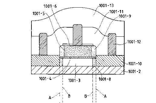
Fig. 10A (or Fig. 17G) is a schematic sectional
view of the structure of an MIS transistor according to
this embodiment, and Fig. lOB is a drawing for
explaining the energy band thereof.
Fig. 17 is a sectional view showing the prodcution
- 40 - 2054~98
1 process in this embodiment. Because Fig. 10A is the
same as Fig. 17G, this embodiment is described below
with reference to the production process of this
embodiment shown in Fig. 17.
As shown in Fig. 17A, à~SIMOX substrate having
a substrate concentration of lE + 16 cm 3 (= 10 6 cm
and comprising a silicon wafer 1703-1, a ground SiO~
layer 1703-2 having a thickness of 5000 A and an Si
layer 1703-3 having a thickness of 500 A was formed
(Fig. 17A).
A gate insulating film 1703-4 of 500 A was then
formed on the SIMOX substrate by thermal oxidation at
900C for 30 minutes. Polycrystalline silicon was then
deposited to 4000 A by the LP-CVD process, and boron was
introduced into the polycrystalline silicon by ion
implantation. A polycrystalline Si gate electrode
1703-5 was then formed by using as a mask material a
resist 1703-7 and Si3N4 1703-6 (Fig. 17B).
First ion implantation was then performed by
using as a mask material the gate electrode 1703-5 for
introducing impurities in source and drain regions
1703-8 (Fig. 17C).
After the resist 1703-7 was removed with leaving
the Si3N4 1703-6, the polycrystalline silicon of 2500 A
was subjected to side oxidation to form a layer 1703-9
(Fig. 17D).
The oxide film and silicon layer in the source
- 41 - 2054498
1 and drain regions were then etched by using as a mask
material the Si3N4 1703-6. During this etching, the
silicon layer 1703-8 was not completely etched, with
leaving a slight portion (for example, about 50 A) of
the layer 1703-8 (Fig. 17E).
A mixed crystal SixGel x 1703-10 was then
selectively deposited to a thickness of about 500 A on
the silicon layer 1703-8 exposed in the source and drain
regions by using a gas mixture SiH4/GeH. The deposited
portion comprised silicon, and the non-deposited portion
comprised a silicon oxide film and a silicon nitride
film. The mixed crystal rate x was 0.1
p31 was then injected by ion implantation
using as a mask the gate electrode (with a polyoxide
film) 1703-S, 1703-9 with an injection energy of 60 KeV
and a dose of lE + 15 cm~2 (= 1ol5 cm~2), followed by
heat treatment at 950C for 20 minutes and thermal
oxidation.
As a result, heterojunctions between Si 1703-8
and Sio lGeO 9 1703-10 were provided in the source and
drain regions so that the heterojunctions were placed
at a distance of about 2500 A from the source-channel PN
junction faces. Namely, the heterojunction faces
(1703-8 : 1703-10) were within the diffusion length
Ld = about 1 ~m from the depletion edges of the PN
junctions (1703-3 : 1703-8) (Fig. 17F).
PSG (phosphorous glass) was then deposited to
_ 42 - 2054498
1 6000 A by the CVD process to form an interlayer
insulating film 1703-11. Wiring Al 1703-12 was
deposited by the sputtering process. PSG was finally
deposited to 8000 A to form a protective film 1703-13
and then subjected to heat treatment at 400C for 30
minutes (Fig. 17G).
The transistor of this embodiment shown in Fig.
10A was produced by the above-described method.
Fig. 10B is a drawing showing the energy band
of the transistor. In the drawing, character A denotes
the heterojunction faces, and character B denotes the PN
junction faces, the region between the junction faces A
and B being a high-concentration impurity regions
comprising the same semiconductor as that of the channel
region. The heterojunction faces A comprise a
semiconductor having a narrow energy band gap.
Fig. 18 shows the results of measurement of the
characteristics of the transistor produced by the above
method in this embodiment.
Fig. 18A shows the Id-Vg characteristics in which
curve 1805-1 shows the results of this embodiment, and
curve 1805-2 shows the results of a thin film SOI-MIS
transistor containing hetrojunctions. As shown in the
drawing, this embodiment shown by the curve 1805-1 has a
good linearity.
In this embodiment, the silicon-germanium mixed
crystal in the source region was Sio lGe0 9 having a
- - 2054498
1 mixed crystal rate x of 0.1 and a mobility of about
2000 cm /v.s which was about twice that of silicon.
This resulted in the formation of a thin film SOI-MIS
transistor having good linearity and high driving force
Gm and exhibiting no deterioration in the driving force
Gm.
Fig. 18B shows the dependency of the driving
force Gm on the gate length. In the drawing, curve
1805-3 shows the results of this embodiment, and curve
1805-4 shows the results of a thin film SOI-MOS
transistor containing heterojunctions. The transistor
shown by curve 1805-4 has the tendency that the driving
force Gm is deviated from an ideal straight line as the
gate length is decreased because the parasitic
resistance of the source and drain regions is made
significant, as compared with the on resistance.
However, the transistor of this embodiment shown by
curve 1805-3 shows the driving force Gm along the ideal
line up to a gate length of about 0.8 ~m.
zo In this embodiment, the endurance voltage
between the source and drain was at least 20 V.
Embodiment 6
A sixth embodiment of the present invention is
described below with reference to the schematic
sectional view for explaining the production process in
Fig. 19.
A ZMR (Zone Melting Recrystallization) substrate
_ 44 ~ 2 054498
1 having a substrate concentration of lE + 16 cm 3
(= 1016 cm 3) and comprising a Si film 1904-3 having
a thickness of 500 A was first formed (Fig. l9A).
A gate insulating film 1904-4 was then formed
on the ZMR substrate by thermal oxidation at 900C
for 30 minutes. A polycrystalline Si was then
deposited to 4000 A by the LP-CVD process, and boron
was introduced therein by ion implantation. A
polycrystalline Si gate electrode 1904-5 was then
formed by using as a mask material a resist 1904-7 and
Si3N4 1904-6 (Fig. l9B).
First ion implantation was performed by using
as a mask material the gate electrode 1904-5 for
introducing impurities into the source and drain
regions 1904-8 (Fig. l9C).
After the resist 1904-7 was then removed with
leaving the Si3N4 1904-6, the polycrystalline silicon of
2500 A was subjected to side oxidation 1904-9 (Fig.
l9D).
The oxide film and silicon layer in the source
and drain regions were then etched by using as a mask
the Si3N4 1904-6. During this etching, the silicon
layer 1904-8 was not completely etched, with leaving a
slight portion (for example, about 50 A) of the silicon
layer (Fig. l9E).
Ge 1904-10 was then selectively grown from the
silicon portion 1904-8 exposed to the source and drain
~ 45 ~ 2 05 ~ q 9 8
1 regions.
p 31 was injected by ion implantation using as
a mask the gate electrode (with a polyoxide film)
1904-5, 1904-9 with an injection energy of 60 KeV and
a dose of lE + 15 cm 2 (= 1ol5 cm 2), followed by heat
treatment at 950C for 20 minutes and thermal oxidation.
As a result, heterojunctions between Si 1904-8 and Ge
1904-10 were provided in the source and drain regions
so that the heterojunctions were placed at a distance
of about 2500 A from the source-channel PN junction
faces. Namely, the heterojunction faces (1904-8 :
1904-10) were within the diffusion length Ld of about
1 ~m from the depletion edges of the PN junction
portions (1904-3 : 1904-8) (Fig. l9F).
PSG (phosphorous glass) was then deposited to
6000 A by the CVD process to form an interlayer
insulating film 1904-11. Wiring AlSi 1904-12 was
deposited by the sputtering process, and PSG was
finally deposited to 8000 A to form a protective film
1904-13, followed by heat treatment at 400C for 30
minutes (Fig. l9G).
As a result of measurement of the properties of
the thus-formed transistor in this embodiment, the
mobility of the source and drain regions was about
4000 cm /Y.S, and good MOSFET characteristics were
obtained in the same way as Embodiment 4.
_ 46 - 2054498
1 Embodiment 7
A seventh embodiment of the present invention
is described below with reference to Fig. 20.
As shown in Fig. 20A, a concave portion of 800
A deep was formed in a portion on a quartz substrate
2008-1 on which MOSFET is formed later. In this
embodiment, the concave portion had a size of 40 x 40
~m. A polycrystalline silicon region of 2 ~m square
was formed at the center of the concave portion. Heat
treatment was then performed in an atmosphere of H2 to
change the polycrystalline silicon region to a single
crystal silicon region 2008-2 by aggregation (Fig.
20A).
Selective growth was then performed by the CVD
process using GeH/SiH4 as a raw material gas and the
2-~m square single crystal silicon region as a seed
crystal (Fig. 20B~.
Selective polishing was then performed by using
as a stopper the quartz substrate 2008-1 to form a
SOI substrate having a single crystal region 2008-4
composed of a mixed crystal Sio lGe0 9 and selectively
formed in the concave portion only. In this embodiment,
as a result of measurement, the thickness of the
semiconductor layer was about 600 A (Fig. 20C).
A silicon oxide film 2008-5 was deposited as a
gate oxide film on the substrate by the CVD process
(Fig. 20D).
_ 47 _ 2 05 1~ 98
1 Polycrystalline silicon was then deposited to
4000 A by the CVD process to form a gate electrode
2008-6. Impurities were introduced by ion implantation
using as a mask the gate electrode 2008-6 to form
source and drain regions 2008-7 (Fig. 20E).
A silicon oxide film was then deposited by
the CVD process for forming a side wall. Anisotropic
etching was then performed to form a side wall 2008-8
having a thickness of about 1000 A (Fig. 20F).
Germanium (Ge) ions were then injected by ion
implantation using as a mask the gate electrode with
the side wall under the conditions of a dose of
2E + 16 cm~3 (= 2016 cm 3) and an injection energy
of 130 KeV. After the ion implantation, heat treatment
was performed at 900C for 30 minutes. As a result,
the region in which Ge ions were injected was composed
0.05 0.95 ( g-
As a result, as shown in Fig. 2OG, the channel
region 2008-4 and the source and drain regions 2008-7
had the following structure:
(1) the semiconductor layer of the channel
region 2008-4 was composed of sio lGeO g;
(2) the source-channel junctions (2008-7 :
2008-4) was homojunctions composed of Sio lGeO g;
and
(3) a region 2008-9 composed of Sio 05GeO 95
with a germanium mixed crystal rate higher than that
- 48 - 2054498
1 of the channel region was provided within a distance
of 1000 A from the depletion edge of the source-
channel junction (2008-7 : 2008-4) on the source side
to form a heterojunction (2008-7 : 2008-9) with the
source and drain regions 2008-7 composed of
Sio lGeO 9.
The diffusion length Ld of Sio lGeO g which
formed the regions 2008-4 and 2008-7 was about 1 ~m
which is longer than the above distance 1000 A.
1 0
"/
~ 49 ~ 2054498
1 An interlayer insulating film 2008-10 was
then formed by the same method as that employed in
Embodiment 6 (Fig. 20~), and metal electrode AlSi
and a protective film were further formed thereon.
As a result of measurement of the characteristics
of the transistor according to this embodiment, the
field effect mobility was as high as about 1200 cm2/v s,
but a good linear region was obtained in the Id-Vg
characteristics.
Embodiment 8
A eighth embodiment of the present invention is
described below with reference to Figs. 21, 22 and 23.
Fig. 21~ is a schernatic sectional view showing
the structure of a SOI-MIS transistor according to this
embodiment, and Fig. 21B is a drawing showing the
energy band thereof. Fig. 22 is a schematic sectional
view for explaining the production process in this
embodiment. Since the sectional view of Fig. 21A is
the same as Fig. 22G, this embodiment is described
with reference to the production process shown in Fig.
22.
As shown in Fig. 22A, a SI~lOX substrate having a
a substrate concentration of lE + 16 cm 3 (=10 cm
and comprising a ground SiO2 film 2203-2 having a
thickness of 5000 A and a Si layer 2203-3 having a
thickness of 500 A was formed (Fig. 22A).
A yate insulating film 2203-4 of 500 A was then
~ 50 ~ 205~998
l formed on the SIMOX substrate by thermal oxidation at
900C for 30 minutes. Polycrystalline Si was then
deposited to 4000 A by the LP-CVD process, and boron
was introduced by ion implantation. A polycrystalline
Si gate electrode 2203-5 was then formed by using as a
mask material a resist 2203-7 and a masking silicon
nitride film Si3N4 2203-6 (Fig. 22B).
Impurities were then introduced by ion
implantation using as a mask material the thus-formed
gate electrode 2203-5 to form source and drain regions
2203-8. Phosphorous (p31~ was used as the impurities,
and the ion implantation was effected under the
conditions of a dose of lE + 15/cm2 (=10l cm2) and an
injection energy of 60 KeV (Fig. 22C).
After the resist 2203-7 was removed with
leaving the Si3N4 film 2203-6, side oxidation of the
silicon of 2500 A was effected to form a side wall
2203-9. As the same time, the impurities was diffused
and activated (Fig. 22D).
The oxide film 2203-4 and the silicon layer
2203-8 in the source and drain regions were dry
etched by using as a mask the Si3N4 film 2203-6. At
this etching, the silicon layer was incompletely
etched with leaving only a small portion (about 50 A)
thereof (Fig. 22E).
Al-Si 2203-10 was selectively deposited to
about 500 A by a lamp overheating method under a gas
- 51 - 20S4498
1 mixture containing monomethylaluminum as a raw material
gas and H2 gas as reaction gas at a substrate surface
temperature of 350C to form a metal electrode for the
source and drain regions only on the silicon portion
2203-8 which was exposed to the source and drain
regions. The deposited portion comprised a silicon
material, and the non-deposited portion comprised a
silicon oxide film and a silicon nitride film. As a
result, the metal electrodes 2203-10 for the source
and drain were placed within a diffusion length Ld f
about 1 ~m from the depletion edges of the PN junctions
(Fig. 22F).
PSG (phosphorous glass) was then deposited to
6000 A by the CVD process to form an interlayer
insulating time 2203-11. Wiring Al-Si 2203-12 was
deposited by the sputtering process. PSG was finally
deposited to 8000 A to form a protection film 2203-13,
followed by heat treatment at 400C for 30 minutes
(Fig. 22ç).
Z0 It was confirmed by sectional SEM (Scanning
Electron Microscope) that the metal electrode 2203-10
in the source and drain portions was extended to the
ground insulating film 2203-2 by subsequent heat
treatment or the like.
The transistor according to this embodiment
shown in Fig. 21A was produced by the above-described
method.
- 52 - 2054498
1 Fig. 2lB is a drawing showing the energy
band of the transistor of this embodiment. In the
drawing, character A denotes heterojunction faces,
and character B denotes PN junction faces, high-
concentration impurity regions being held between
the junction faces A and B. The metal electrode
2203-10 is present from a turn at the face A where no
forbidden band region such as a semiconductor region
is present.
Fig. 23 is a drawing showing the device
characteristics of this embodiment.
Fig. 23A is a drawing showing the Id-Vg
characteristics in which reference numeral 2304-1 shows
this embodiment, and reference numeral 2304-2 shows a
comparative example of thin film SOI-MOS transistors.
In this embodiment, since the metal electrodes in the
source and drain regions are extremely close to the
source-channel junction edyes, as compared with the
source-drain electrodes in a conventional transistor,
the parasitic resistance is very low, and a good
linearity is thus obtained. The driving force (the
slopes of the courves shown in the drawing) is increased
about twice.
Fig. 23B is a drawing showiny the dependency of
the driving force to the gate length. In the drawing,
curve 2304-3 shows the results of this embodiment, and
curve 2304-4 shows the results of a thin film SOI-MOS
~ 53 ~ 2054~98
1 transistor used for comparison. The comparative
example shows a deviation from the ideal line (the
one-dot chain line shown in the drawing) as the gate
length decreases. This represents that the parasitic
resistance in the source and drain portions becomes
significant, as compared with the on resistance. While
the transistor of this embodiment shows the dependency
along the ideal line up to a gate length of about 0.8
~m. This shows that the parasitic resistance is
sufficiently low.
Fig. 23C is a drawing showing the Id-Vg
characteristics. In the drawing, curve 2304-5 shows
the results of this embodiment, and curve 2304-6 shows
the results of a thin film SOI-~OS transistor used for
comparison.
Fig. 23D is a drawing showing the relation
of the distance between the metal electrode of the
source region and a source-channel PN junction to the
source-drain endurance voltage. As shown in the
drawing, the source-drain endurance voltage of this
embodiment is 20 V or more and is significantly
improved, as compared with the convertional transistor.
Embodiment 9
A ninth embodiment of the present invention is
described below with reference to Fig. 24.
As shown in Fig. 24A, polycrystalline silicon
was deposited on a quartz substrate 2405-1, and the
205~98
- 54 -
l polycrystalline silicon film formed was molten and
solidified by applying an laser thereto to form a
single crystal layer 2405-2. As a result, a SOI
substrate having a semiconductor layer with a thickness
of 500 A was formed (Fig. 24A).
A silicon oxide film 2405-3 having a thickness
of 300 A was then formed on the substrate by the
thermal oxidation method, and Si3M4 2405-4 was deposited
to 200 A on the oxide film 2405-3 by the LP-CVD
process to form a two-layer gate insulating film (Fig.
24B). -
Polycrystalline silicon was then deposited to
5000 A by the LP-CVD process to form a gate electrode
2405-5. Phosphorous (P ) ions were then injected
into the source and drain regions 2405-3 by using as
a mask material the gate electrode 2405-5 with a dose
of lE + 15/cm2 (=10l5/cm2) and an injection energy
of 60 KeV (Fig. 24C).
After the source and drain regions 2405-3 was
formed, the polycrystalline silicon which formed the
gate electrode 2405-5 was oxidized to deposite a CVD
silicon oxide film thereon, and the spacer (side wall)
2405-7 shown in Fig. 24D was formed by anisotropic
etching (Fig. 24D).
The spacer 2405-7 was then subjected to dry
etching so as to have the sectional structure shown
in Fig. 24E (Fig. 24E).
~ 55 ~ 205 q~98
l WSi (tungsten silicide) 2405-8 was then deposited
over the whole surface by the sputtering process (Fig.
24F).
The WSi was then lifted off by the silicon oxide
film by a wet etching process using a hydrofluoric acid
etching solution (Fig. 24G).
An inter layer insulating film 2405-9, metal
wiring (WSi) 2405-10 and a protective fime were then
formed by the same method as that employed in the
seventh embodiment. As a result, a i~OS transistor
having metal electrodes 2405-8 which were provided
within the diffusion length Ld from the PN junction
faces and which were extended to the quartz substrate
2405-l having the ground insulating film was formed
(Fig. 24H).
As a result of comprison of the transistor
of this embodiment with a comparative thin film SOI-
MOS transistor, the SOI-MOS transistor of this
embodiment showed no kink phenomenon and had a source-
drain endurance voltage of 20 V or more and the Id-Vg
characteristics with good linearity.
Embodiment 10
A tenth embodiment of the present invention is
described below with reference to Fig. 25.
As shown in Fig. 25A, polycrystalline silicon
was deposited on a quartz substrate 2506-l by the LP-
CVD process and then molten and recrystallized by
- 56 - 2054498
1 applying an eximer laser thereto to form a semiconductor
silicon layer 2506-2. The thickness of the semiconductor
layer was adjusted by sacrifice oxidation. A SOI
substrate having the semiconductor silicon layer 2506-2
having a thickness of 500 A was thus formed. 200 A gate
oxide film 2506-3 having a thickness of 200 A was then
formed by the thermal oxidation method (Fig. 25A).
A polycrystalline silicon film was then
deposited to 4000 A by the ~P-CVD process to form a
gate electrode 2506-4, and impurities were introduced
into source and drain regions 2506-5 by ion implantation
using as a mask the gate electrode 2506-4 (Fig. 25B).
The polycrystalline silicon which formed the gate
electrode 2506-4 was then thermally oxidized to form a
polycrystalline silicon oxide film 2506-6 having a
thickness of 2000 A (Fig. 25C).
A resist 2506-7 was then applied for forming
contact holes, as shown in Fig. 25D (Fig. 25D).
The contact holes were forr.led with self alignment.
In this formation, the contact holes could be formed
with self alignment without being short-circuited with
the gate electrode by etching the oxide film in an
amount of 400 A (Fig. 25E).
As shown in Fig. 25F, aluminum was then
deposited by the sputtering process of form source-
drain metal electrodes 2506-8 and subjected to heat
treatment at 470C.
57 ~ 2054498
l As a result, the device had the sectional
structure shown in Fig. 25G in which the aluminum
of the metal electrode 2506-8 was extended to the
quartz substrate having the ground insulating film
2506-l. In this embodiment, the important points
were the following:
(l) Al is used as the source-drain metal
electrode 2506-8 without using AlSi.
(2) The temperature of the heat treatment
after the deposition of the Al electrode 2506-8 is
470C.
These points purposely produces an Al spike
phenomenon.
As a result, the source-drain metal electrodes
2506-8 are disposed within the diffusion length of l
~m from the source-channel PN junction faces, and the
metal electrodes 2506-8 are extended to the ground
quartz substrate 2506-l. A PSG film was then deposited
to 8000 A to form a protective film.
A recrystallized silicon thin film SOI-MOS
transistor was formed by the same method as that
employed in this embodiment with the exception that a
metal electrode was formed of AlSi, and the temperature
of heat treatment after the metal electrode was
deposited was 400C and compared with the transistor of
this embodiment. As a result, it was found that the
transistor of this embodiment has an improved endurance
- 58 - 2054498
1 voltage and Id-Vg characteristics with a good linear
region.
As described above, in the present invention,
since the energy band gap Eg2 in the source portion is
set to a value different from the energy band gap E
in the channel portion, holes are smoothly moved
between the source and channel, and good saturation
properties and a high source-drain endurance voltage
can be obtained.
In addition,-in a thin film SOI-MIS transistor
having heterojunctions in the source and drain regions,
the heterojunction faces are provided within the
diffusion length Ld from the depletion edges of the
source-channel PN junctions, thereby obtaining the
effects of improving the resistance to the kink
phenomenon and the source-drain endurance voltage and
decreasing the dark current.
The MIS transistor of the present invention
produces no phenomenon that the dark current is
increased due to the generation of the current from
defects which serve as generation sources or paths (for
example, hopping current), as in a conventional
transistor in which the source-channel PN junctions are
heterojunctions, or heterojunctions are included in the
2S depletion layers of the PN junctions.
Further, a thin film SOI-MIS transistor formed
by using as a semiconductor material a mixed crystal of
~ 59 ~ 2054498
1 silicon and germanium and having a heterojunction
provided at least in a source region is characterized
by the following:
(1) The mixed crystal rate y of the channel
portion (SiyGel y) is greater than the mixed crystal
rate x of the source and drain portions (SixGel x)' the
mixed crystal rate x satisfying the condition that x
< 0.12;
(2) The SixGel_x heterojunction face of the
source portion is provided within the diffusion length
Ld from the depletion edge of the source-channel PN
junction on the source side.
There are thus the effects of decreasing the
parasitic resistance of the source and drain regions
and increasing the driving force Gm with preventing
the deterioration thereof even in a MOS transistor
formed on a thin film SOI substrate having a thickness
of as small as 500 A.
The invention also has the effects of preventing
the kink phenomenon and increasing the source-drain
endurance voltage.
Further, in a thin film SOI-MIS transistor, a
metal electrode of a source portion is provided within
the diffusion length Ld from the source-side depletion
edge of the source-channel PN junction and is extended
to the ground insulating film, thereby improving the
resistance to the kink phenomenon and the source-drain
- 60 - 2054498
1 endurance voltage, significantly decreasing the
parasitic resistance of the source and drain portions
and preventing the deterioration in the driving force.
Although each of the embodiment uses a SIMOX
substrate, SOI substrates which can be formed by
other methods can of course be used.