Note: Descriptions are shown in the official language in which they were submitted.
'~/O 91/14329 1 P~/S~ 6
DIRECT PHASE DIGITIZATION
BACKGROUND OF THE INVENTION
The present invention relates to the detection of the phase
and/or frequency of a signal, such as a received radio signal,
rel~tive to a known reference signal, as is more particularly
concerned with a method and apparatus providing a digital
indication of the detected phase or frequancy of the received
signal.
The instantaneous phase or the instantaneous frequency of an A.C.
electrical signal or pulse train is o~ten preferred to be
directly available in digital form when subsequent numerical
processing is to take place thereon with the aid of microcom-
puters or digital signal processing chips, for the purposa of,
for example, demodulating a phase or frequency modulated radio
signal.
Phase and frequency have a close mathematical relationship such
; that frequency is the time derivative of phase. If a device is
; available for digitizing phase, a digital representation of
freguency can therefore under certain conditions be obtained by
numerical differentiation of the phase using modulo 2Pi
~circular) arithmetic subtraction. Alternatively, a frequency
digitizing device under certain conditions may be used to
generate a digital representation of phase by numerical re-
integration using modulo 2Pi (circular) arithmetic addition. In
both cases, success depends on an accurate mapping of the
; circular phase domain onto a circular digital domain or Galois
field of the same 2Pi period. For example, if an 8-bit binary
word is çhosPn to represent phase, the number range 0 to 256 must
exactly match the phase range 0 to 2Pi radians so that the phase
wrap-around over 2Pi is exactly represented by the wrap-around
of the 8-bit binary word back to 0 upon incrementing 255 by 1.
.
A conventional method to digitize the phase of an A.C. electrical
signal is to apply the signal first to a phase comp~rator along
with a reference signal, the phase comparator thus producing an
output voltage or current proportional to the phase difference
- ~ ' '
'' ' ' .
Wogl/14329 2 PCT/SE91/OOlS2
7 6 ~
between its inputs. This analog measure of the signal phase ~ay
then be applied to an analog-to-diqital converter in srder to
generate the desired numerical value in the form o~ a digital
code.
The above-mentioned method has certain drawbacks, apart ~rom the
need for analog circuit components. If the phase-to-voltage
conversion factor of the phase comparator does not exactly match
the voltage-to-code conversion fact:or o~ the A-to-D converter,
an error occurs in the mapping of one circular domain to the
other, which can become magnified in subsequent numerical
processing such as differentiation.
A similarly conventional ~ethod of digitizing frequency by means
of an analog frequency discriminator followed by an A-to-D
converter suffers from a similar drawback. When the ~requency
is r~-integrated to obtain phase, the results diverge from the
true phase due to practical tolerances in the matching of the
discriminator to the A-to-D conver er.
When the input signal contains a significant amount of noise,
there are a limited number of phase comparator circuits with a
2Pi range which function correctly. For example, it is not
desirable to use a phase comparator which averages the ~hase of
the signal over many cycles, as, in the region of the 0/360
degrees discontinuity where successive phasas ~ay alternate due
to noise between just over O and just less than 360 degrees, such
a circuit can produce completely wrong average result of 180
degrePs. In order to solve this problem of averaging ~ circular
quantity such as phase, its instantaneous value is required.
Circular averaging may then be employed, which involves ta~ing
the sine and cosine of the phase angles, averaging those
separately, and then computing the arctangent of the result.
An alternative solution to the modulo 2Pi problem for noisy
signals is to use two phase comparators with their reference
inputs offset by 90 degrees so that at least one of them lies far
from the ambiguous region. A type vf phase comparator is often
"; ,' :~
, ;-:
. . ..
WO91/14329 3 PCT/SE91/00152
~ ~ ~i /1 7 ~ ~i
chosen which produces an output voltage propor~ional to the sine
of the phase di~ference between its inputs, ~he two quadrature
co~r~rator outputs then bein~ a measure of the sine and cosine
of phase angle, respectively. These signals are ~uitable
directly for circular averaging. Then, after separate digitiza-
tion of the averaged sine and cosine signals, ~he desired phase
number may be obtained by a numerical arctangent operation. This
so-called I,Q (In-phase and Quadrature) m~thod, is quite complex,
as it requires a nu~ber of analog components, two A-to-D
conversions and a numerical arctangent operation.
A known method to produce a value representing the instantaneous
frequency of a signal using purely digital logic ~lements is the
so-called counter-discriminator method. This method entails
directly counting the n~mber of zero-crossings ~or cycles) of the
input signal which occur in a given time. After reading out the
previous result, the digital counter is reset to zero and then
proceeds again to count ~ero-crossing events of the input signal
for a fixed time to produce the next number.
The problem associated with the counter-discriminator is the long~~ 20 count time needed to determine the frequency with pr~cision. For
example, if l~ measurement accuracy is ragulred, the count time
1 must span around lO0 zero-crossings of the input signal. The
; rate at which new frequency measurements can then be generated
is limited to around l/lO0 of the signal frequency. Moreover,
fluctuations of the signal frequency within the measurement
period will not be seen.
The drawback associated with the digital counter-discriminator
is partly due to the need to limit the timing resolution to whole
; cycles of the input signal. If fractional cycle resolution could
be obtained, a given mea~u~l ?nt accuracy can be reached in a
shorter time. In digital period measurement, the duration of one
or more whole cyc:les o~ the signal is measured by counting cycles
of a much higher frequency clock, thus providing fractional cycle
accuracy. The reciprocal of the period is a measure of the
frequency.
. .
:
, .-:
. WO9l/14329 ~ PCT/SE91~W152
7 ~ ~
In digital period measurement, occurrence of a signal z~ro-
crossing causes the previous count to be read out of the counter
bPfore resetting it to zero. It then counts again until the next
zero-crossing, at which point the new period measurement is read
out, and so on.
The drawbacks associated with digital period measurement are the
need for the rec~procal operation, and the fact that the period
for which the mea~'- nt ap~lies is not regular, but determined
by the signal itself. This operation is referred to as natural
sampling. It is more often desired to sample and digitize the
signal at regular sampling intervals that are not a function of
the possibly noisy or varying signal.
SUMMA~Y OF THE lNv~NllON
The present invention is directed to an electronic circuit that
directly generates, at intervals which may be specified, values
which correctly represent in modulo 2Pi format the phase angle
of an A.C. signal or pulse train relative to a reference clock
signal or pulse train. Furthermore, the phase values generated
are suitable for numerical differentiation or other processing
using modulo 2Pi arithmetic in order to generate digital
representations of instantaneous frequency.
.
A particular feature of the circuit according to the present
invention is that the input signal frequency, reference clock
frequency, and phase sa~pling frequency may be independently~ 25 chosen, within practical limits, and are not constrained to have
particular relationships therebetween. A further feature of the
circuit according to the present invention is that ~he circuit
may be configured entirely with digital logic elements.
It is therefore an object of the present invention to provide an
electronic devic~e which generates at ~pecified time intervals
digital values which represent in modulo 2Pi for~at the instan-
:, ~
:. ,
.. .. ~
WO91/14329 5 PCTtSE9~/00152
~5~7~
taneous phase angle of an AC signal relative to a reference ciocksignal.
It is a further object of the present invention to provide an
electronic device which is capable of performing numerical
differentiation of the instantaneous phase angle value produced
using modulo 2Pi arithmetic in order to genera~e digital value
representations of instantaneous frequency of the AC 6ignal.
It is another object of the prese!nt invention to proYide an
electronic device which produces the digital value representation
of the instantaneous phase angle of the AC ~ignal wherein the
input signal frequency, the reference clock frequency, and the
phase sampling frequ~ncy are independently chosen and are not
required to have particular relationships therebetwPen for
; utilization by the electronic device in deriving the instan-
l~ taneous phase angle value.
.
It is still further an object of th~ present inventio~ to provide
an electronic device which produces digital values of either
instantaneous phase or instantaneous frequency of an input AC
signal which oveLco ?~ the previously mentioned drawbacks of
conventional phase/frequency digitization devices.
These and other objects are achieved by the present invention
which provides an electrical circuit for determining at specified
sampling instances a numerical value which represents as a
digital code an instantaneous phase of an electrical signal
relative to a reference frequency signal. A counter circuit is
provided for conti~uously generating a stored count representing
a value resulting from dividing the reference freque~cy signal
by a repeatin~ count cycle frequency, the count cycle repetition
frequency being of the same order as an expected center frequency
of the electrical signal. A trigger unit is provided for
producing a trigger pulse in response to the trigger unit
receiving a sampLing pulse at an arming input and a transition
of the electrical signal at a firing input. An intermediate
register stores a momentary state of the counter circuit in
, . ' . ~ , ;
,.: .
-~
W091~14329 6 PCT/SE91/00~i2
2~5l~7~i
response to the intermediate register re~eiving the trigger
pulse. The momentary state of the counter circuit corresponds
to an instantaneous phase value of the electrical signal. A
correcting circuit is provided for correcting a r~sulting
numerical value in the intermediate register by removing an
accumulating phase offset ~alue, the phase o~f~et v~lu~ being a
product of a predetermined time pericd between ~ampling pulses
and a predetermined frequency between the count cycle repetition
freguency and the expected center frequency of the electrical
signal. ~n o~ register is provided for ~toring the corrected
resulting numerical value of the counter circuit w~ich is
transferred from ~he intermediate register in response to the
oc~ ence of the next sampling pulse, which also effects a
storage of the next momentary state of the counter circuit in the
inte -~;ate register.
BRIEF DESCRIPTION OF THE DRAWINGS
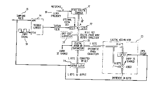
Fig. l illustrates a block diagram of the digitization circuit
according to the present invention;
Fig. 2 illustrates a preferred e~bodiment of the trigger circuit
according to the present invention;
Fig. 3 illustrates a block diagram of a further embo~; -nt of the
digitization circuit according to the present invention;
Fig. 4 illustrates a block diagra~ of the digitization circuit
according to the present invention including a non-linear
correction unit and a frequency estimator: and
Figs. 5a and 5b illustrate alternate embodiments of the frequency
estimator according to the present invention.
DETAILED DESCRIPTION OF THE PR~KR~ EMBODIMENTS
Referring now t~ Fig. l, a simplified block diagram a circuit
which implements the principles of the present invention is
shown. A reference clock frequency l0 is generated which is an
integer multiple, preferably binary, of the expected ~ignal
frequency. The reference clock frequency lO is applied to a
digital counter 12 which divides the reference clock frequency
,- :
,
:~ .
.. . .
Wo 91/14329 7 PC~tSE91/00152
7 ~ ~
by this integer multiple to produce a divider count cycle which
repeats at the same rate as the expected signal frequency. An
ou~ value is produced by recording the state of the counter
12 at zero-crossing events of the input signal. In contrast t~
the above-mentioned known methods, the digital counter 1~ is not
periodically reset and continuss to increment betwee~ measure-
ments. ~oreover, recordinq o~ the coun~er ~ta~e i~ caused by a
trigger circuit 14 which is initiated in response to ~he
oc~L~ence of two e~ents.
The trigger circuit 14 must first be armed by receipt of a
sampling pulse 16 which indicatss that a measurem~nt is to be
made. Once armed, the trigger circuit 14 is fired by the
occurrence of the next zero-crossing of the input signal 18. The
c,uLpuL trigger pulse 20 produced by the trigger circuit 14 when
it is fired causes the state of the counter 12 at that instant
to be transferred to an intsrmediate holding register or latch
22. As an optional embodiment, an extra bit of timing precision
~ may be obtained by extPn~ing the latch by one bit and recording
also whether the reference clock frec~ency 10 at the trigger
instant was on a negative or positive half cycle. Optionally
this addition may be improved to extend the timin~ accuracy by
more than one bit by using a reference signal waveform having
more than just two possible voltage states, ~or example a
'. sawtooth or other analog waveform, and quantizing its state to
a much higher accuracy tha~ one bit by such means as an A-to-D
converter.
.
The contents of the intermediate latch 22 are held until the next
sampling pulse 16 is applied to arm the trigger. circuit 14, at
which point the contents are transferred to a digital
adder/subtractor 25 and subsec~ently to an ouL~L register or
latch 24 before they become replaced by the next meaa~ nt.
Measurements thus appear in the ouL~uL register 24 with a one-
sample delay, and at a regular rate determined by the externally
applied samplinc; pulse 16.
. .
,.
WO91/14329 8 PCT/SE91/00152
~0~'17~
If the expected signal frequency is exactly equal to the division
cycle repetition frequency of counter 12, zero crossings will
always occur at the same reference counter ~tate, which in turn
depends on the arbitrary phase of the signal relative to ~he
S reference clock ~requency lO~ For example, assuming the counter
12 divides by 64, the seguence of~- h~rs produced by the counter
12 may be 29j 29, 29...
I~ the expected signal freguency is lower than that o~ the
division cycle repetition frequency, then zero crossings will
occur progressively later at each sampling event, for example,
29, 32, 35, 38...62, l, 4, 7..., the counter wrapping around at
the value of 63.
The exact expected increment per sample is, in this example,
i equal to 64 times the frequency offset multiplied by the time
between samples. For example, if the expected n in~l signal
frequency is lO00 Hz lower than the reference counter repetition
frequency, and the sampling rate is 256 Hz, then the expected
increment between samples will be lO00/256 - 3 29/32nds.
- When the input signal no i nal center frequency is equal to the
repetition period of the N-bit digital reference counter, i.e.
equal to fO divided by 2N, assuming the counter is pure binary,
then successive phase measurements will give the same value. In
practice a reference clock having an ou~y~ frequency exactly 2
times the expected no in~l input signal frequency is often not
readily available, therefore it is desired to use instead the
nearest available frequency. This error is fixed and known, so
one can predict in advance that the resulting phase measurements
will be in error by an amount which progressively increases
between successive samples.
For example, if the difference between the reference frequency
divided by 2N (the reference divider repetition counter cycle)
and the nominal input signal frequency is lO0 cycles per second,
the phase measurements would change at the rate of lO0 times 2Pi
per second even with an ex.act cPntral input frequency. If the
.
.
- wosl/l4329 9 PCT/SE91/OV152
7 ~ ~
sampling rate is looo per second, the phase error is thus
increasing at the rate 100*2Pi~1000 = Pi/5 between each sample.
This progressively increasing, but totally predictable error can
be removed by the circuit shown in Fig. 1.
S The above example wherein the count~er 12 wraps around the value
of 63 has been chosen where ths expected increment 3 29~32nds is
not an integer in order to illustrate that the cumulative
in~ nt can nevertheless still be predicted by exten~ing the
precision to the right of an imagine~d decimal point to represent
the fractional part. In the above examp~e, a bina~y ac~l lator
23 having six bits to the left of the decimal point plus five
bits to the right of the decimal point may be used to represent
nl h~rs in steps of 1/32nd. The ac -lator would be incremented
after every sample by the digital code:
000011.11101 representing 3 29/32nds.
The digital accumulator 23 is incremented after e~ery sample
pulse by the known systematic phase error increase per sample
period, i.e. Pi/5 in the above example, so it rotates progres-
sively through the values Pi/5, 2Pi/5, 3Pi/5, 4Pi~5, 0 (the carry
is ignored), Pi/5, etc. The value in the accumulator 23 is then
subtracted from the phase measurement by a digital
adder/subtractor to produce a corrected result which again would
be a constant value on successive sample pulses for an exact,
nc in~l input frequency. The mean rotation due to the systema ic
frequency deviation of the reference clock frequency lO from an
exact relationship with the input signal center frequency is
thereby removed.
It can be appreciated that the word length in bits o~ the
accumulator 23 can be as large as necessary to represent
fractional frequency errors to as high a precision as desired.
The accumulator 23 can have more bits of precision than the N or
~+l bit phase measurement recorded in the intermediate latch 22.
In principle, only the most significant N or N+1 bits of the
accumulator 23 would then be used in the digital adder/subtractor
25 to effect the correction, however, to reduce the small extra
,. . . , . .
. ,~ ..
.
WO91/14329 lo PCT/SE91/001~2
20~7~
error associated with ~runcating the accumulator value used, it
can be advantaye~us to use one or two extra ~its over and above
N (or Ntl) with the result that the precision of the output value
from the adder/subtractor 25 is extended to L bits in length,
S where L is slightly more than N ~or N~l) e.g. N~ bits. In the
casa where the ~ystematic frequency error can be exactly
represented by an ac~i lator inc~ ~nt of no greater precision
than N or ~1 bits, then it is not nec~ss~ry to extend the
accumulator or the adder~subtractor word length.
The value in the accu~ulator 23 represent~ the systematic phase
offset a signal at exactly the specified nominal center ~rec~ency
would have accumulated up to this point due to systematic
frequency offset ~rom the reference. The inc~ ?nt to the
ac~ ator 23 represents the extra phase rotation that is added
every sampling cycle due to the systematic frequency offset
integrated over the sampling interval. By subtracting the
ac_ _lated phase offset from the ph~se measurement b~fore
transferring the result to the output register 24, it is
corrected both for systematic frequency error and for the non-
commensurate sampling rate. It therefore bec- ?5 possible to
choose the signal center frequency, reference frequency and
sampling rate independently of each other, within reasonable
practical limits. It is further possible to have a varaable
period between samples, providing the irregularity is systematic
and known, so that the systematic phase error component can be
predicted and subtracted out.
The digital counter 12 of Fig. 1 is preferably one utilizing
"Grey Code". A Grey code count sequence is one in which only one
digit of a multi-digit counter changes between each count. For
example, the decimal sequence - 0,1,2,3,4,5,6,7,8,
9,19,18,17,16,15,14,13,12,11,10,20,21,22,23 - is Grey coded. In
binary, the difference between Grey code and normal binary is
exemplified as follows:
-. , .
. ,- :~ , ,:
Wo9l/~432s 11 PC~/SE91/00152
7 ~ ~
Normal Binary Grey Coded Binary
0 0000 0000
1 0001 0001
2 oolo ooll
3 0011 OQ10
0100 0110
0101 0111
6 0110 0101
7 0111 0100
8 1000 1100
9 1001 1101
10 1010 1111
11 1~11 1110
12 llOo lOlo
13 1101 1011
14 1110 1001
15 1111 1000
With normal binary coding, if the trigger pulse occurs exactly
~ at the instant the counter 12 is incrementing, several digits can
; 20 be changed at once, e.g. the transition from 0111 (7) to 1000
(8). There is the danger that the bits change at finite and
; sliqhtly different speeds. This transition may cause a false
valu2 to be latched in which some of the bits have been changed
and others have not. For eXample, in the transition from 0111
(7~ to 1000 (8), if the most significant bit changes slightly
faster than the r~ ing bits, the erroneous state 1111 (15)
could possibly be latched. By using ~rey coding, however, only
one bit changes at a time. Therefore, the only two alternatives
that can be latched if the trigger pulse occurs at the time the
counter 12 is changing are the previous value and the new value,
either of which is equally viable. Wh n a Grey coded counter
sequence is used, a Grey-to-binary conversion is nee~e~ to
facilitate the performance of subs~quent arithmstic such as
addition/subtraction on the phase value. Therefore, it is
convenient to utilize a Grey-to-binary converter 26 at a point
between the intermediate latch 22 and the G~ latch 25.
The trigger circuit 14 required in Fig. 1 may be implemented
according to the logic diagram illustrated in Fig. 2. Referring
thereto, a firsl; edgè-triggered (D-type) latch 26 has the
sampling pulse source 16 connected to its clock input, and a
.
.
WO9ltl4329 12 PCT/SE9l/~l52
20~l~7~
permanent '1' level on its data input. Upon occurrence of the
sampling pulse edge, the data '1' level will be transferred to
the Q ou~uL, which is further connected to the data input of a
second edge-triggered latch 28. The clock lnput of latch 28 is
driven by the input signal 18. Thu~;, upon occurrence o~ the next
edge or zero-crossing of the input signal 18 after the trigger
circuit 14 has been armed, a '1' level will appear on the Q
ou~u~ of the fire latch 28. This ou~pu~ is the trigger pulse
ou~u~ to the intermediate latch 22 required in ~ig. 1.
When the trigger circuit 14 has fired, the trigger circuit 14 is
reguired to be Le~u-ned to its initial state by means of a
suitable reset pulse. Thi's may, for example, be produced by
delaying the trigger pulse from the Q output of the fire latch
28 through two shift registers 30 which are clocked at the high
reference clock frequency 10 to produce a reset pulse to both the
arming latch 26 and fire latch 28. Since the trigger pulse from
the fire latch 28 has no special time relationship with the
reference clock frequency 10, it can occur shortly before a
reference clock edge resulting in little or no delay in it
appearing out of the first shift register delay stage. Two shift
register delay stages are therefore utilized to guarantee that
the output trigger pulse and reset pulse are at least one
reference cloc~ cycle long and do not occasionally become
vanishingly short.
A number of possible further embodiments of the present invention
may be implemented. A previously mentioned alternate embodiment
consists in obtaining one or more extra bits for precision in
the phase measurement by recording in the intermediate holding
latch 22 not only the counter 12 state at the instan~ the trigger
pulse occurs, but also the state of the reference clock waveform
at the trigger instant. In the simplest implementation of this
e hod~ ent, ther,e need only be the high/low state of a square
wave clock waveform which is recorded to provide an extra bit of
resolution. For further increasing resolution, a waveform having
more than two vo:Ltage states, such as a staircase or continuous
ramp (sawtooth wave) can be used, together with a device to
~ '
.
:, ... .
;
.: .
! WO 91J14329 13 PCT/SE91/001~2
2~7~
discriminate between the different states for example, a suitable
A-to-D converter. -
It can further be advantageous to use both positive and ne~ativegoing edges or zero-crossings of the input signal.- One advantage
may be gained by allowing the trigger circuit 14, after being
armed, to be ~ired by edges of either polarity, whichever arrives
first, the advantage being that it is the edge nearest in time
to the desired sampling instant which ~s phase-quantized. In
this case, it is ~lso nece~sAry to record which polarity fired
the trigger, and to correct the phase value obt~ineA by O or 180
degrees accordingly, for example, by inverting the most sig-
nificant bit (MSB).
Fig. 3 illustrates one configuration of the pre~ent invention
using both edges of the input signal to trigger the digitization.
The occurrznce of a sampling pulse lS simultaneously arms two
distinct trigger circuits 30, 32 that may then be fired upon the
occurrence of, respectively, a positive going or negative going
transition of the input signal 18.
The ouL~uL trigger lines are logically ORed by OR gate 36 so that
the occurrence of either trigger effects latch;ng of the
reference counter state into the first latch 22. Moreover, the
occurrence of this event resets both trigger circuits 30, 32 so
that a new sampling pulse 16 is needed before they again can be
fired. This operation guarantees that only the first to be fired
after arming will be fired. A set/reset flip-flop 34 records
which of the two trigger circuits 30, 32 is fired.
Assuming that it is the positive going transitions of the input
signal which defines phase, and that negative going transitions
occur nominally mid-way between (180 degrees), then it i5
necessary to correct the phase measurement by 180 degrees if the
measurement was made on the negative going signal ~dge. This
correction is done by inverting the most significant bit of the
phase measurement by way of an XOR gate 38 by EXCLUSIVE ORing the
flip-flop 34 stiate with the MSB (which represents O or 180
.~. .
- ................ .
.
- .
WO9l/]4329 14 PCT/SE91/00l52
~5~76~
degrees) if a nPgative transition fired the joint trig~er before
latching the result in the output latch 24 at the next occurrence
of a sampling pulse.
A slight advantage in phase resolution or accuracy may be
5 obtained by using two ~eparate trigger circuits triggered
respecti~ely by the negative and positive going ~lanks of the
input ~ignal, and to record the counter ~tate separately in two
distinct latches. The two results may then be combined to result
in a phase word having one bit of e~ra length. The combination~0 of the two results may be performed for example as follows:
PHASE = MOD2~(2*A t MODn(B-A~)
where A is the content of the latch triggered by zero-crossings
o~ one polarity (measured modulo n, probably a power of two) and
B is a si~ilar value from the latch triggered by zero-crossings
of the other polarity.
The difference B-A calculated modulo n is added to twice the
value of i~ ~A left-shifted ons bit). The result reduced modulo
2n gives a phase representation of one bit greater word length.
Furthermore, by arranging that no strobe is produced to the
ou~yuL latch 24 unless the trigger circuit 14 was fired in the
last sampling period, the previous value may be held in the case
that the input signal was anomalous or too weak to provide a
better estimate. Higher order holding algorithms ~ay also be
implemented either by c~ FuSing numerical derivatives within the
phase digiti~ing circuit, or in subsequent numerical processing.
In the latter case, a flag bit would be generated from the
circuit to indicate whether a trigger pulse had occurred or not
during the last sa~pling period.
In addition, an alternate embodiment of the present invention
includes an arithmetic unit which receives the corrected digital
value stored in the ouLyu~ latch 24 in order to generate a
digital code which represents an instantaneous ~requency value
of the input sign,al. The unit is operable for subtraction of two
successive instantaneous phase values using modulo 2Pi arith-
,
.
W091/14329 l5 PCT/SE91/001~2
' 205~76~
metic, which in effect is equivalent to a differentiation of theinstantaneous phase value.
As the phase of the input signal 18 relative to the available
frequency reference lO and/or the sampling clock pulse 16 is
arbitrary, the actual occurrence of a zero-crossing of the input
signal 18 may be offset in time from the desired ~a~pling instant
by up to nominally one cycle of the frequency of input signal 18,
in the event that zero-crossings o~E only one polarity ~re used,
or up to nominally hal~ a cycle in the event that both polarities
are used. This sampling timing error in turn gives rise t~ an
error in the phase measurement equal to the extra phase rotation
of ~he input signal 18, due to its fre~uency difference from the
reference clock frequency lO, multiplied by the extra time. If
the resulting O-l cycle or O-l/2 cycle time ~itter is small
cc -red to the sampling period and the frequency offset of the
signal is small relative to the reference clock frequency lO,
this extra error is proportional to the product of two small
quantities and therefore may be neglected. If, however, either
quantity is significant, such as when the system is designed to
operate with a larger syste~atic offset between the input signal
nominal frequency and the reference clock freguency, or when the
- sampling rate is a significant fraction of the input signal
frequency, or both, it can become nacessary to perform an
explicit correction to remove this form of error.
2S The required correction is the product of the amount of time dT
occurring earlier or later than the desired sampling instant at
which the trigger is fired, expressed as a fraction of the total
sa~pling T, with the expected phase offset dF of the signal over
the entire sampling period. This correction is expressed in the
following equation:
Extra Correction = dF*dT~T
As an example, the situation when the desired sampling instances
are coincident with the reference counter value being O will now
be described. In this case, dT is given by the phase value
latched in the intermediate latch 22. Otherwise, dT would be
: ' -
.
~ . .
. .
Wo91/14329 l6 PCT/SE91/~152
7 ~ ~
given by the intermediate latch value minus the value of thedigital counter 12 at the occurrence of the sampling pulse lS.
The phase offset dF of the signal relative to the reference that
occurs during a sampling period is proportional to the frequency
offset. It may be sufficient to use only the fixed n ;n~l value
of the expected systematic frequency of~set. Alternatively, in
the case of an input signal whose frequency varies ~ver a wide
ranqe, it may be necess~ry to use an estimate of the instan-
taneous frequency. In an embodi~ent in which the present
invention is utilized for ~requency determination by numerical
differentiation of the phase measurPment, such an estimate will
already be available. A block diagram of an embodiment of the
present invention illustrating such a method of applying the non-
linear correction is illustrated in Fig. 4.
With respect to the embo~i ~nt using the non-linear correction
of Fig. 4, an optional non-linear correction unit 40 may be
regarded as a supplemental component to the digi~al accumulator
utili~ed in the embodiment of Fig. l. It ~hould be noted,
however, that it is not necessary to use the digital ac_ tator
technique in order to apply the non-linear correction unit 40.
The digital accumulator 23 of Fig. l calculates a systamatically
increasing (rotating) phase value corresponding to the difference
in frequency between the expected signal and the reference
counter value. This value is then subtracted from the measured
pha~e to obtain a corrected phase value which is approximately
equal to the value that would have been obtained if the reference
counter 12 had a period equal to that of the n~ i n~l siqnal.
The aforementioned correction suffices if a large time jitter on
the trigger pulse relative to the desired re~ular sampling
instance does not occur. Moreover, if there is a significant
time jitter on the occurrence of the trigger pulse, but little
or no systematic freguency error to remove, then the non-linear
correction may be dispensed with. However, when both the timing
jitter and the systematic frequency offset are significant, the
non-linear correction method depict~d in Fig. 4 may be desirable,
~ ,
. ~ ' .
, ~:
- : ~
,: -
:., ~ ~, , .
.
- WO 91/14329 17 PCI'/SE91/00152
2 ~
as the magnitude of the non-linear effect i5 proportional to the
product of the ~ime error dT and the ~requency of~set dF.
The non-linear correction unit 40 of Fig. 4 includes an
adder/subtractor 42 and a multiplier 44. A frequency estimator
46 is provided in order to prolduce frequency estimates and
includes a comparator 47, an ac~l lator 48, and a loop filter
49.
In order to carry out the non-linear corrQction, an estimate of
the frequency offset dF is ~ee~ed for multiplication with dT, the
sampling time error. Fig. 4 illustrates the use of the frequency
estimator 46 in a method of estimatin~ the instantaneous
fre~uency error, and is otherwise referred to as a digital phase~
lock loop. The frQguency estimator 46 simultaneously estimates
any static systematic frequency offset plus any dynamic, varying
component, due for example, to modulation applied at the sending
end of the input signal. Of course, if the static, systematic
component is already known ~eforehand, as is the case when the
digital accumulator 23 of Fig. 1 is used, it could be removed by
such a digital accumulator technique before applying the result
to the digital phase-lock loop of Fig. 4, which would then only
estimate the residual dynamic component. The dynamic component
would then be added to the static component to get the total
instantaneous frequency error dF which is applied to the non-
linear correction unit 40. If the dynamic component is small,
and the static component is relatiYely large, it may be adequate
to only use the static component for the value of dF in the non-
linear correction. Since the digital phase-lock loop, however,
estimates both the static and dynamic c~ ~onents of the instan-
taneous frequency offset, the digital accl t~ator 23 is not
necessary in all situations.
; The desired final result of the circuit illustrated in Fig. 4 is
in fact a measure of the instantaneous deviation of the signal
frequency from an already known nominal value. The digital
phase-lock loop of the frequency estimator 46 produces a measure
of the instantaneous deviation of the input signal 18 from the
.'~
.. . . .
: . .,
, . . ~ ~ .
WO9l/14329 18 PCT/S~91/00152
20~7~
reference counter frequency, which is equal to the desired
deviation from the no~in~1 fre9uency plus the constant difference
- of the nominal freguency relative to the reference counter
frequency. Therefore, the constant difference from the reference
frequency, if not zero, would be ;~ubtracted ~rom the frequency
estimate dF be~ore delivering the desired result to further
processing. In this case, a constant value correspn~ding to the
static frequency offset would have been subtracted from a
frequency measurement, instead of, as in Fig. 1, subtracting an
increasing phase correction from the phase -~-q~re~ent. I~,
however, a phase o~ut value is desired fxo~ the system of Fig.
4, the corrected phase value from non-linear correction unit 40,
if necessary, may be combined with the ou~uL o~ a digital
accllr-llator as in Fig. 1 in order to subtrac~ out the systematic
offset caused by a known static frequency error.
Figs. 5a and 5b illustrate devices for deriving frequency
estimates from resulting phase measurements, and each of the
devices illustrated by Figs. 5a and 5b may be used as an
alternative e~bodiment for the frequency estimator 46 of Fig. 4.
Fig. 5a illustrates a devic~ for deriving frequency estimates
from phase measurements by numerically s~btracting successive
input samples. The device of Fig. 5a determines the rate of
;~ change of phase angles by subtracting adjacent phase angle
measurements made one sample period apart~ An n-bit subtractor~ 25 52 subtracts a delayed phase measurement O/i-L from a current
phase measurement 0/~. The delayed phase measurement O/i-L
results from a phase measurement passing through delay units 50
which delay the phase measurement by a predetermined number of
sampling periods. The end result is then passed through a
digital filter 54 which in turn ou~pu~s the frequency estimate
-~ desired.
The device of Fig. 5b derives frequency estimates from phase
measurements by utilizing a digital phase-lock loop circuit. The
device subtracts, by way of n-bit subtractor 56, incoming samples
of phase measurement values from a val~e contained in an
'
. ' . ~' "
~ ,, '
'
.' ''' ~ ' : '
W091~1432g 19 PCT/SE91/00152
~ 5~76
accumulator 57. The accu~ulator S7 measures the angular error
between the incoming phase samples and the stored value, and
corrections are implemented by a corrPction u~t 58 in order that
the two values become aligned. The resulting alignment thus
produces an estimate of the rotation frequency o~ the sequence
of input phase angles. If the input freguency is constant, the
output result will be accurate to the n1 ~er of digits of the
arithmetic used. If, however, the rate of rotation of the phase
angles in the input sequence i6 not perfectly constant, e.g.
noisy radio signals, the ac~ lator 57 and correction unit 58
will continually correct the error between the input sequence and
~alues and the stored values. Thus, the resulting estimate will
only be that of the input frequency at that particular moment.
While a particular mbo~i ~nt of the present invention has been
described and illustrated, it should be understood that the
invention is not limited thereto since ~odifications may be made
by persons skilled in the art. The present application con-
templates any and all modifications that fall within the spirit
and scope of the underlying invention disclosed and claimed
herein.
. , ~ .: .
. ;. :