Note: Descriptions are shown in the official language in which they were submitted.
S91362
2 0 ~ ~14 2
BAC~GROUND OF THE ~ .lON
1. Field of the Inventlon:
The present inventlon relates to a llquid
crystal display apparatus for forming a seamless com-
posite picture from a plurality of liquid crysta}
display panels thraugh optical fiber transmission.
2. Description of the Prior Art:
In recent years, a variety of display appara-
tus have been used, among which a liquid crystal dis-
play apparatus is becoming more popular than the con-
ventional CRTs because of its thin structure, relative-
ly small consumption of electricity, and versatility.
However, a ~iquid crystal display apparatus has a
disadvantage inherent to its intricate construction in
which liquid crystal is confined in spaces of micron
order between transmissive picture elements. The
dlsplay panels are susceptible to dirt, ther~by caus-
ing fau~ty picture elements. As the size of the dis-
play apparatus becomes large, faulty pic~ure elements
are more likely to occur. Faulty picture elements
spoil the commercial value of a display apparatus.
Tests show that when the size of a screen is 15 inches
or more, mass production at a reasonable production
costs b~co~s difficult.
In order to overcome this problem, a plurali-
ty of minor liquid crystal display devices, having a
diameter of 15 inches or less, are arranged so as to
constitut~ a large-size apparatus. An example is shown
in Figure la in which nine minor display devices 1 are
arranged in a lattice (3 x 3). If each device 1 is a
S91362
- - 2 - 20~5142
14 inches type, the fintch~ dlsplay apparatus will be
a 42 ~cho~ size.
A small display unit like the display
device 1 unavoidably has a non-lmage area 1~ along the
periphery of the screen, wherein the non-image area has
no lmage represented. This non-image area having a
wldth of 3 mm is unavoidably formed by a space for
containlng liquid crystal confined between the two
opposing substrates, a~d a space for disposing the
wiring a~d electrodes for applying voltage to the
picture elements.
Because of the non-image area ths resulting
composite picture is spoiled by seams as shown in
Figure la. What is worse, it is likely to cause a
fa~al wrong communication of data.
In order to solve the problems ~entioned
above, there are proposals which are disclosed in
Japanese ~aid-Ope~ Patent Publication Nos. 63-250680
and 63-}75882. Figure 2 shows the display device shown
in the 63-250680 Publication. This deYice includes
optical fiber bundles 15 to 18 disposed in correspond-
ence to picture elements in minor screens 11 to 14.
The optical fibers are individually connected to the
minor screens 11 to 14 at one end each thereof, and the
other ends are bundled so as to constitute a major
screen 10. The 63-250680 Publ~cation discloses a
similar type of display device.
~ owever, because of the spaces among the
screens 11 to 14, a mis~lignment is likely to occur
S91362
~ 3 ~ - 20~5142
between the ma~or screen 10 and the mlnor screens l~-to
14. This necessitates the bend~ng of the optical
fibers at portions 15 to ~8, which causes the ~ollowing
problems:
As shown in Figure 3, if the optical
fibers 19 having the same length and a diameter of d
are bent at an angle ~ at portions l9a equally distant
from one end each thereof, the bending of the optical
fibers causes a deviation o~ d x t~n (~/2) between the
outside corner lgb and the inslde corner l9c. More
speciflcally, in the drawing, the inside corner l9c
rises above the outside corner l9b by d x tan (a/2).
With this s1tuation, if the optical fibers are consecu-
tlvely stacked, the ~ent portions l9a shlft upward.This ca~ses misalignment in the ends of the optical
fibers 19. The misalignment of the optica} f i~er ends
must be made up for by ~illing ln the gaps or ~y pro-
longing the short optical flbers until all the ends are
evenly aligned. As a result, the length L' between the
minor screens la and the ma~or screen 20 in Figure 4 is
~isadvantageously prolonged.
SUMMARY OF THE lN~ lON
The liquid crystal display panel of this
lnvention, which overcomes the above-discussed and
numerous other d~sadvantages and deficiencies of the
prior art, includes at least two display devices each
having screens, an optical fiber bundle connected to
the respective screens so as to transmit an image
therethrough, wherein the optical fiber bundle com-
prises optical fibers arransed side by side and fas-
S91362 20~51~ 2
tened to each other to take the form of a letter Yhaving a stralght portion and branch port~ons, the
stralght portion belng perpendlcularly connected to an
output end face, and the branch portions belng connect-
ed to an input end face, and spacers interposed between
adJacent optical fibers in a portion of the bundle at
least toward the output end face.
In a preferrsd embodiment, the optical fibers
have a core whose refractive index is an even step
index type, and whose numerical aperture is not small-
er than the angle of expanslon of a light from picture
elements.
In a preferred embodiment, a light transmis-
sive plate is disposed on a face on which a composite
image is formed by the optical fiber bundle.
In a preferred embodiment, the optical fibers
have a core whose refractive index is an even step
index type, and whose numerical aperture is not small-
er than the angle of expansion of a light from picture
elements, and further comprising a light transmissive
plate disposed on a face on which a composite image is
formed by the optical fiber bundle.
Alternatively, the liquid crystal display
apparatus including three display devices each having
screens, a first and a second display device being
spaced from each other and thelr screens being on the
same level, the third display device being located
rearward of the first and second display devices toward
the input slde of the display apparatus and having a
S91362
- ~ 5 ~ 2055142
screen rearward thereof, and an optical fiber bundie
interposed between the first and sa~-o~d display devices
and ~on~ected to the screen of the third display device
at the inp~t end, and the output end face thereof being
located between the screens of the first and second
display devlces so as to transmit an image there-
through, wherein the optlcal fiber ~undle comprises
optlcal fibers arranged side by slde, fastened to each
other, and bent so as to enable each end portion of the
optical fiber bundla to be connected perpendicularly to
the input and output screens, and spacers interposed
between ad~acent optlcal fibers in a portion of the
bundle at least toward the output end face.
In a preferred embodiment, wherein the
screens of the first and second display de~ices com-
prise light transmissive plates having a refractive
index approximately equal to that of the cores in the
optical fibers.
In a preferred embodiment, wherein the angle
of expansion of light at the output ends of the optical
fibers is approximated to that of each picture element.
In a preferred embodiment, wherein the angle
of expansion of light at the output ends of the optica~
fibers is approximated to t~at of each picture element.
Thus, the invention described herein makes
possible the o~jectives of (1) providing a ~iquid
crys~al display apparatus capable of forming a seamless
composite picture from a plural~ty of display devices,
and (2~ providing a liquid crystal display apparatus
~91362
_ - 6 -
2055142
capable of displaying a clear and ~right picture on a
large screen.
BRIEF DESC~PTION OF T~E DRAW~NGS
~ h~s invention may be better understood and
its numerous ob;ects and advantages wlll become appar-
ent to those skilled in the art by reference to the
~ompanying drawlngs as follows:
Figure la is a front view showing z plurality
of screens used in a conventional liquid crystal dis-
play apparatus:
igure lb is a ront view showing one of the
screens;
Figure 2 is a perspective view showing a
li~uid crystal display apparatus with a conventional
structure using optical fibers;
Figure 3 is a schematic view exemplifying a
problem of the convsntional liquid crystal display
apparatus shown in Figure ~,
Figure 4 is a schematic view explaining
another problem of the liquid crystal display apparatus
shown in Figure 2:
Figure 5 is a front view showing a f irst
example of the liquid crystai display apparatus accord-
ing to the present invention;
S91362
~ 7 ~ 2055142
Figure 6 is a flowchart showing a driving
clrcu~t used in the liquid crystal displ~y apparatus
shown ln Flgure 5;
S Figures 7a to 7d are schematic views show-
ing a signal processed by the dr~ving circuit,
Figures 8a to 8f are diagrammatic views show-
~ng the steps for processing signals of the drivlng
c~rcuit;
Figure 9 ls a sectlonal view showing an
optical fiber bundle used in the liquid crystal display
apparatus in Figu~e 5;
F$gures lOa to lOh are diagrammatic view
showing the steps for fabricating the optica} bundle
shown in Flgure 9;
Figures ~la and llb each are fragmentary
views on an enlarged scale showing examples of the
optical bundle;
Figure 12 is a front view showing ~nother
example of the present invention;
Figure 13a is a schematic view exemplifying
the state of a light when black resin is not used in
the optical bundle;
Figure 13b is a schematic view showing the
state of a light when black resin is used in the ~pti-
cal bundle;
Sgl362
-- 8 --
- 2055142
Figure 14 ls a front vlew showlng a further
exzmple of the present invention;
Figure 15 ls a front view showing a still
further example of the present inventlon;
~ igures 16a to 16f are dlagrammatic views
showing the steps for processing signals in the liquid
crystal di~play apparatus in Figure 15;
Figure 17 ls a perspective view showing a
modified optlcal fiber;
Figure 18a is a schematic view show~ng the
relationship between the numerical aperture and the
difference in refractive index between the core and the
cl~ing of the optical fibers;
Figure 18b is a ~chematic view showlng the
angle of expansion of the light from picture elements;
Figure 19 is a schematic view showing an
example for arranging the optical fibers in relation to
the picture elements:
Figure 20 is a sc~ tic view showing another
example for arranging the op~ical fibers in relation to
the picture elements;
Figure 21 is a schematic v~ew showing an
example in which a g~ss panel is used to facilitate
the ~ixing of the optical fibers; and
S91362
2Q55142
Flgure 22 ~s a sectional view showing a
structure of the input end face formed by the optical
flbers.
DESCRIPTION OF THE PREFERRED EMBODIMENTS
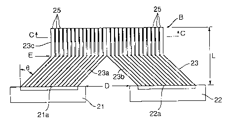
Referring to Figure 5, the liguid crystal
display apparatus is provlded w~th two li~uid crystal
d~splay devices 21 and 22 but the number of display
devices are not limited to tw~ pieces. The dlsplay
devices 21 and 22 are respectively provided with
screens 21a and 22a which are horizontally aligned and
~ace frontward. Each screen 21a and 22a hss a display
face ~. An optical fiber bundle 23 is connected to
the screens 21a and 22a. The optical fiber bundle 23
is separated into branch portions 23a (rlght field) and
23~ (left ~ield~ at a plane E so as to take the form of
a reversed letter Y. More specifically, the branch
portions 23a and 23b are connected to the display
face D of the respective screen 21a and 22a at an
angle ~.
In this way the optical fiber bundle 23 takes
the form of reversed Y, that is, branch portions 23a
and 23b and a straight portion 23c where spacers 25 are
inserted between ad~acent optical fibers. The
spacer 25 will be hereinafter described in detall. The
other end of the optical fiber bundle 23 has a display
face s which is formed with the allgned equally spaced
ends of the optical fibers.
When the display devices 21 and 22 are driven
through a driving circuit by split signals for the two
S91362
-- 10 -
2055142
f~elds, the pictures appear~ng on the screens 21a and
22a are displayed as a cG.~o~ite picture on the display
face ~ without discontinuity. The picture qual~ty is
enhanced irresp~ctlve of the enlar~ement.
Figure 6 is a block diagram showing a drlving
circuit for driving the display devices 21 and 22. The
c~rcuit includes an A/D converter 31 to which an analog
slgnal (image signal) taken by a solid photographing
device (not shown) is app}ied, a synchronous signal
separator 32 for separating a synchronous signal from
an output of the A~D converter 31, and a left-field
memory 33 for storing a signal applled to the
left-field from the signal from the A/D converter 31, a
risht-field memory 34 for storing a signal applled to
the rlght fleld, a left signal processor 35 and a rlght
signal processor 36. The left signal processor 35
outputs a left LCD video signal to the dlsplay de-
vice 22 allotted to a one frame picture on the basis of
the signals from the memory 33 and the separator 32.
The rlght signal processor 36 outputs a right LCD video
signal to the display device 21 allotted to the one
frame picture on the basis of the signals from the
memory 34 and the separator 32. Hereinafter, the LC~
video signal will be referred to as the "video signal".
The operation of the drlving circuit will be
described by using an example in which image data is
processed for a one f~ame picture:
In Figure 7a, suppose that the ~llustrated
letter A is a one frame picture to be displayed, and an
image signal concerning th~s image A is input to the
S91362
2QSS142
A/D converter 31 whlch ~n turn outputs an image slgnal
shown ~n Figure 8a. F1 shows a one field portion.
Synchronous signals trl and tr2 are separated from the
output of the A/D converter 31 by the separator 32 as
shown in Flgure 8b.
The half of the remzining picture portion
allotted to the left field is enlarged by exp~ g the
picture wldth Xl in Flgure 8a to the width X2 so as to
be fully displayed on the whole screen 22a, and stored
in the left-f~eld memory 33. The other half of the
remaining picture portion allotted to the right field
is likewlse enlarged as shown in Figure 8d, and stored
~n the right-field memory 34.
Afterwards, the left signal processor 35
mixes the signal from the memory 33 and ~he synchronous
slgnals trl and tr2 sepasated by the separator 32, and
outputs a left field image data as a left video signal.
At the same time, the rlght signal processor 36 mixes
the signal from the memory 34 and the synchronous
signals trl and tr2 separated by the separator 32, and
outputs a right field image data as a right video
signal.
The display device 22 (left picture use~
d$splays a left portion of the intended pic-
ture A (Figure 7~) in response to the left vldeo sig-
nal, and the display device 21 (right picture use~
displays a right portion of the intended pic-
ture A (Figure 7c) in response to the right video
signal. The picture displayed by the display
devices 22 and 21 is transmitted to the display face ~
S91362
-- 12 -- -
20551~2
through the optical fiber bundle 23 . The seamless
comp~1te picture A is dlsplayed on the display face B
es shown in Figure 7d.
The optical fiber bundle 23 will be descrlbed
n detail by referenre to Figure g to 11:
The optical fiber bundle 23 ta~es the form of
reversed letter Y as shown in Figure 5, and is provided
with the spacers 25 inserted between the ad~acent
optical fibers so as to maintain proper gaps therebe-
tween. Figure 9 shows a cross-section of each optical
fiber 27. As shown in Figure 9, an appropriate number
of optical fibers 27 are arranged side by side in a
row, and an appropriate number of rows are arranged
with the spacers 2~ interposed therebetween. The rows
are referred to as optical fiber ~ands 28a below. ~he
spacer 25 is made from a sheet material. The reference
numeral 26 denotes black paint packed in the gaps so as
to shield light.
The optical fiber b~ndle 23 can be fabricated
as follows:
In Figure lO an appropriate number of optical
fibers 2~ are arranged side by side and bonded to each
other so as to fo~m a single sheet-like integer, here-
inafter referred to as the "sheet 28". This sheet 28
is cut to a desired width Wl and length W2 as shown in
Figure lOb. The tape-like spacers 25 are bonded 2t
equal intervals on one side of the sheet 28 as shown in
Figure l~b. The width W1 is determined so as to be
equal to that of the screens 21a and 22a of the display
S913~2
- 13 - 20~S142
devices 21 and 22.
Then, the optical fiber bands 28a are ob-
tA~ne~ from the sheet 28 by cuttlng the sheet 28 lnto
optical f~ber bands 28a each having the spacers 25
along one edge thereof as shown in F~ gure lac . As
referred to above, the optical fiber bands 28a consti-
tutes the rows. Than, as shown in Figure lOd, the
optical fiber bands 28a are bent at a predetermined
distance from the end. The bent optical fiber
bands 28a are stacked into a block 30 as shown in
Figure lOe. ~he length W3 of the b~ock 30 ls equal to
that of the screens 21a and 22a.
Two blocks 30 are prepared, and joined to
each other as shown in Figure lOf, wherein the optical
fiber bands 28a are releasab~y bonded to each other
under the bonding force of the adhesive used in forming
the sheet 28. The spacers 25 are f~rmly bonded with a
suitable adhesive referred to below.
The~, as shown in Figure lOg, the black
resin 26 is fllled in the gaps prese~t in the
blocks 30. The black resin is made of epoxy resin, for
example. The black resin absorbs any light which
otherwise would be likely to enter ad;acent optlcal
fibers, and cause detrimental light interference. The
ad~antage of the black resin will be described in
greater detail below. Finally, as shown in Figure lOh,
each top face is flatly cut to form the display faces B
and D. In this way, the optical fiber bundle 23 is
flnished. The advantages of th~s optical fiber
bundle 23 are (1) that a seamless picture is displayed
S91362
- 14 -
20~5142
on the display face B and (2) that the length L can ~e
shortened. Ths reason why the length L can be short-
ened is explalned as follows:
In Figure lla, each branch portion 23-a and
23b of the optical fiber ~undle 23 is expanded more
w~dely by an angle ~ than the straight portion 23c.
As a result, the op~ical fibers of the branch
portlon 23a and 23b have a longer dlameter by (d/cos ~)
~o than that of the straight portions. Because of this
d~fference between d snd (d/cos ~) planar gaps occur in
the display face B. The planar gap has a thickness of
d(1/cos ~-l). According to the present invention, the
spacers 2~ fill in this gap, thereby allowing the
dis~cord between the bent point Al of the left optical
fiber 27a and A2 and the bent point A2 of the centrai
optical fiber 27b. ~hus the length L can be shortened
with the ends of the optical fibers 27 aligned on the
same plane. It is preferred that the curvature is as
small as possible so as to shorten the length L. In
the drawing the bent optical ~lbers 27 are represented
in straight lines, but actually they are bent along
smooth curved lines.
The values of the length L depend upon many
factors; for example, when the interval between the
display devlces 21 and 22 is 20 mm, the optical fiber
bundles 23 are bent at an angle of 20, and the screens
21a and 22a have a diameter of 20 inches, it is
32.5 mm under the present invention. Under the same
conditions, the length L will ~e 83.0 mm under the
conventional structure. When the screens 21a and 22a
have a diameter of 30 inches, the length L is 32.5 mm
S91362
20551~
accordlng to the present invention in contrast to
~08.3 mm under the con~entlonal structure.
When the fabrlcation of the spacers 25 having
the same thickness as that of the planar gaps is dlffi-
cult, especially when the extremely thin spacers are to
be fabricated, two spacers 25a and 25b are provided on
the parts of the display faces B and D as shown ln
Figure llb, with the difference between the thicknesses
of the spacers 25a and 25b being equal to the size of
the planar ga~s. The elastirity of the spacers 25, 25a
and 25b can be taken into consideration if they are
made of elastic material.
The spacers 25, 25a and 25b are made of
tough, workable and machinable material which can be
used when the thickness is less than 100 ~m. For
example, polyester, polyamide, polyethylene, polyethyl-
ene naphthalate, polypropylene, and acetate can be
selectively used. In the illustrated example, polyes-
ter having a thickness o~ 25 ~m was ~sed.
Example 2
Referring to F~gure 12, the optical fiber
bundle 40 is twice bent $n a plane E and a plane ~ each
at an ang~e of ~. The difference from Example l is
tha~ branch portions 40a and 40b are bent in the
plane F, and connected to the screens 21a and 22a at a
right angle. A straight portion 40c has the display
face B.
Spacers 41 and 42 are provided at two places,
that ~s, on the parts of the displ~y faces B and D. In
S91362
- 16 --
.
20S51~
Example 2, the length L can be shortene~, and the
pt cture dlsplaced on the dlsplay face B is seamless.
In Example 2, black resin is fllled in the
gaps. A greater advantage of black resin also results
as shown ln Flgure 13~ as compared with a case where no
black resln is used as shown ln Figure 13a. In that
case, when a li~ht a is $ntroduced into the optical
fib~r bundle 40, a light component b passes throush the
optlcal fibers 27 but a light component c introduced
at a larger angle than the prescribed angle is likely
to enter optical fibers other than those through which
it was introduced. This causes light leakage, thereby
impcverishing the picture quality.
In contrast, in Figure 13b the light compo-
nent c is absorbed in the black resin 26, thereby
p~e~entins detrimental l~ght interference from occur-
ring. The black resin is filled in the same manner and
at the same places as in Example 1.
The embo~im~nt shown in Figure }4 is provided
with a transparent plate 43 such as glass panel adhered
to the display face 3, so as to enhance optical charac-
teristics, and protect the display face B against dirt.
Even if any dirt sticks to the display face B, it is
readily cleaned on the transparent plate 43. The
transparent plate 43 protects the display fac
against mechanical shocks. When plastic-made optical
fibers are used, the transparent plate 43 is especially
useful for protecting the plastic optical fibers.
S91362
- - 17 -
20S5142
~xample 3
Referring to Flgure 15, a third example will
be descrlbed:
This example ls different from Examples 1 and
2 in that another dlsplay devlce 45 is provided between
the display devices 21 and 22. The third display
devlce 4~ has a screen 45a. The p~cture which is
formed on the third screen 45a is transmitted to an
area in which no picture can be formed on the
screens 21a and 22b by the display devtces 21 and 22.
The screens 21a and 22b include an ordinary screen
inherently needed, and in addltlon to it, transparent
plates 43a and 43b, respectively, which have surfaces
on the same level.
The optical flber bundle 40 has a special
structure so as to increase the density of the optical
fiber bundle in the narrow gap between the display
devices 21 and 22. This special structure will be
described 2S follows:
~ asically, this optical fiber bundle 40 is
constructed so as to be located in the narrow gap
between the display devices 21 and 22. To achieve
this, the bundle 40 is bent in planes E, E', F and F'.
More specifically, as shown in Figure ~5, the optical
fiber bundle 40 is first bent in a plane F below whlch
the bottom end of the bun~le is perpendicularly con-
nected to the screen 45a. The bundle 40 is bent in twoplanes E and E' so that the portion between these two
planes is converged so as to pass through the narrow
gap between the display devices 21 and 22. The
S91362
-- 18 -
~055 1 4~
bundle 40 is agaln bent ln a plane F' so t~ ~e ~b~p
end of the bundle 40 is perpendicularly connected to
the display face B. Spacers (not shown) are provided
between the planes D and F, and between the planes Fl
and B. The descript$on of the manner of providing the
spacers ls omltted for simplicity.
Figures 16a to 16f are tlming diagrams show-
ing the steps for processing the signals in the dlsplay
apparatus according to the present invention.
In Figure 16a an image data obtained by a
sol$d photographing device is input for one frame.
Then as shown in Figure 16b synchronous signals trl and
tr2 are separated from the image data, and on the ~asis
of the synchronous signals trl and tr2 further synchro-
nous signals tr3 and tr4 are formed ~Figure 16c).
These synchronous signals tr3 and tr4 divide the image
data on an lmage to be transmitted to the display
devlces 21, 22 and 45. The synchronous s$gnals trl to
tr3 form an image da~a for the left field (Figure 16d),
and the synchronous signals tr4 to tr2 form an image
data for the right field ~Figure 16f).
The image data for the left field is deliv-
ered to the display device 22, and an image data for
the central field is delivered to the display
device 45, and the image data for the right field is
delivered to the display device 21. Thus a seamless
picture is formed on the display face B.
Figure 17 shows a modified configuration of
an optical fiber suitable for use in Examples 2 and 3.
S91362
-- 19 --
- 2055142
This modifled opt$cal fiber 27 lncludes a stem portion,
and thlck portions 27a and 27b at the lnput end and
the output end. The thick portions 27a an~ 27b can be
round or elliptical.
Figure 18 shows the structure and the optical
characterist~c of the opt$cal flbers 27. In the exam-
ple shown in Figure 18a, the numerical aperture is
shown in terms of a difference between refractive
~0 indexes of a core 27d and a clad portion 27e of each
optical fiber 27. The numerical aperture is defined as
sin (~/2) by obtaining the valus of ~, where the
angle ~ is an incident angle at which a light is intro-
duced into the optical fiber 27 from a lisht source
such as display device 21 or picture elements. When
this incident angle ~ is ad~usted to be equal to the
angle ~ in Flgure 18b or larger than it, the light of
picture elements 46 is introduced into the optical
fi~ers 27. Thus a bright and clear picture ~s dis-
played with good resolution.
As is evident from the foregoing descr~ption,When the angle ~ in terms of the numerical aperture is
larger than an angle of expansion ~ of a light from
picture e~ements, any angular deviation at the input
end face will be compensated, and is prevented from
inflicting unfavorable influence on the resulting
image. I n the e~ho~ment shown in Figure 5 the branch
portions 23a and 23b are slantly connected to the
screens 22a and 23a ~ut when ~he picture is viewed from
the f ront, it is seen bright. In the embodiment shown
in Figure 15, when the angle ~ is equal to the angle of
expansion ~, the resulting pictures formed by the
S91362
- 20 -
- - 2055142
dlsplay devices and transmitted through the optical
fiber bundle 40 have no seam or boundary, ~hereby ob-
taining a good quality co~posite image. In this case,
the optical fibers are preferably an even step index
type, that i8, the cores thereof have an e~ual re~rac-
tive index.
Wh~n the image is represanted in color, the
optical fibers are arranged for the picture elements in
the following manner:
Figure 19 shows an example in which each of
picture elements 46 fo~ red (R), green (G), and
blue (B) ls provided with a single optical fiber 27.
Figure 20 shows an example in which three picture
elements for three colors, that is, red (R), green (G),
and blue (B) are provided with a single optical
fiber 27 so that li~hts from the three picture elements
are transmitted through the single optical fiber 27.
In thls case, the arrangement shown in Figure 21 is
preferable. Under this arrangement a light is trans-
mitted by the display device 21 through the optical
fiber 27, and the picture elements whose image is to be
displayed are made to correspond to the arranoement of
the target picture elements, thereby enabling the
boundary between the pictures to disappear. Thus a
good quality composite plcture is obtained. To achieve
this, it is additionally required that the glass
plate 43 is provided with grooves 43a in which the
optical fibers 27 are secured as desired.
In the case of Fi~ure 21 it is not always
necessary to locate the optical fibers 27 exact~y at
S91362
- 21 -
2055142
pos~tions correspondlng to the ~icture elements 46,
because adJacent other optical fibers 27 compensate for
any positional deviatlon between the optical fibers and
the plcture elements. Thus the occurrence of poor
lmage quallty is prevented.
The optical fiber can be more advantageously
made of plastic than quartz, ~ecause of its lnexpenslve
price, toughness, workability, anti-shock abllity,
light-transmlss$bility. In addition, a core having a
minute diame~er of 0.1 mm to 0.5 mm can be easily made
in a plastic optical fiber.
The optical fiber bundle is fixad to the
display faces B (the output end) and D (the input end)
in various manners. A typical method is to fill resin
in the gaps between the optical fibers arranged. When
plastic optlcal fibers are used, the difference in
coefficient of expansion between the filed resin and
the optical fibers can be minimized, thereby avoiding
the deformation of a display image due to changes in
temperature.
It is preferable that the optical fi~ers have
2~ a cross-se~tional area occupying 50% to 90% of the
total opening of the optical fiber bundle. This is
advantageous in the numerical aperture and a wide range
of light expansion. It is also preferable that the
optical fibers are fixed with the use of light-absorb-
ent resin.
Figure 22 shows an example which makes up foran uneven face D formed by variously term$nating ends
S9l362
- 22 -
20S5142
of the optlcal fibers 27, therPby maintalning the
quality of a composite picture. ~he gaps occurring
between the variously termlnating ends of the optical
flbers and the screen 21a and 22a are filled with a
transmissive liquid 50 having a high refractive index.
If the refractlve index is n, the optical unfavorable
influence can be reduced to l/n. The selection of a
liquld having a particular refractlve index allows the
control of the brightness of the picture as desired.
The method of filling in the gaps with a liquld 50
reduces the burden to connect the optical fibers to the
dlsplay device in sn airtight manner. It is possible
to apply pressure mechanically to the connection of the
optical fibers and the display device but the screen
and optical fibers are liable to breakage under the
pressure.
It is understood that various other modifica-
tions will be apparent to and can be readily made by20 those skilled ln the art without departing from the
scope and spirit of this invention. Accordingly, it is
not intended that the scope of the claims appended
hereto be limited to the description as set forth
hereln, but rather that the claims be construed as en-
compassing all the features of patentable novel~y thatreside in the present ~nvention, including all features
that would be treated as equivalents thereof by those
skilled in the art to which this invention pertalns.