Note: Descriptions are shown in the official language in which they were submitted.
,, , . CA 02055208 2000-04-07
A OUANTUNI BARRIER SEMICONDUCTOR OPTICAL DEVICE
This invention relates to a low operating current long-
wavelength region quantum barrier semiconductor optical
device superior in temperature characteristic.
Prior Art:
Well-known semicanductor laser diodes (LD) for long
wavelength region optical communications are double hetero-
structure LDs with a C3aInAs(P) active layer and an InP clad
layer, which area put in practical use as light sources for
trunk optical communication lines.
Longwavelength region laser devices are fitted with a
Peltier device when applied to trunk line systems since they
are inferior to shortwave length region ones in temperature
stability.
Lasing threshold current IT"of laser diodes is
expressed as function of temperature T by equation:
ITH = ITHO x exp (T~TO) . . . . . . . . . . . . (1)
wherein T, To represent operating temperature and
characteristic temperature in Kelvin respectively.
As is seen in eq(1), high To = values mean superior
stability of threshold current in wide temperature range.
For example:, shortwavelength region laser diodes
exhibit characteristic temperature To > 150K. In the case
of longwavelengt:h region laser diodes, on the other hand,
their characteristic temperature To marks 130-140° K
1
24~~~~~
below the temperatures less than approximately 10 °C but
lowers to 60 - 80° K above the temperatures approximately
°C ,
The following three mechanisms have been considered as
causes of low characteristic temperature of longwavelength
region laser diodes.
1 - 1 Thermal excitation and diffusion leakage of
electrons from the active layer to the clad layer:
1 - 2 Leakage of hot electrons excited in the conduction
band by Auger CHCC process and over flow to the clad
layer.
1 - 3 Increase of light absorption due to the excitation
of holes in valence band by Auger CHHS process.
Of the above, 1-2 is said to be a main cause of
lowering the characteristic temperature in longwavelength
region laser diodes.
The reasons for regarding 1-2 as main cause of lowering
characteristic temperature To (K) are as described in
literature-1 titled:
G.P. Agrawal et al.: Longwavelength Semiconductor
Lasers, Van Nostrand Reinhold Company, pp. 70 - 138
that the leakage current increment via (1-1) is as small as
less than 100 A/~ in the 1.3 a m region and that light
absorption increase via (1-3} do not sufficiently elucidates
actual dependence of current on temperature.
20~~~UB
How to decrease the electron overflow caused due to
Auger effect is therefore of key importance in improving
temperature characteristic of longwavelength region laser
diodes.
From this standpoint of view, use of DCC (double
carrier confinement) and MQB (multi-quantum barrier) methods
have been studied to improve temperature characteristic of
Iongwavelength region laser diodes.
Mentioned in literature-2:
M. Yano et al.: IEEE J. Quantum Electron. vol. QE-19,
pp. 1319-1327
is DCC type laser diodes as shown in Figs. 4(a) to (c) with
cross sectional structure, energy band diagram and
temperature characteristics of threshold current.
The DCC structure in Fig. 4(a) is fabricated by growing
and forming n-Inp clad layer 2, a first GaInAsP active layer
3, a p-InP middle clad layer 4, a second p-GaInAsP active
layer 5, a p-InP clad layer 6, a p-GaInAsP contact layer 7,
an n-InP block layer and a p-electrode 9 in the order of
mention on an n-TnP substrate 1.
The laser diodes with such a DCC structure as shown in
Fig. 4(a) show improved characteristics temperature of 130
to 210° K up to about 80°C as is shown in Fig. 4(c) and also
exhibit reduced temperature dependences of the differential
quantum efficiency.
,, , , CA 02055208 2000-04-07
The reason for such an improved temperature
characteristic of DCC structure LD is that the hot electrons
overflowing from the first active layer generating the main
part of the gain required for lasing are scattered by the
middle clad layer to lose energy and captured by the second
active layer to contribute again to stimulated emission.
Therefore, the DCC structure in Fig. 4(a) produces the
effect equivalent to the reduction of effect
1-2.
In MQB type devices, super lattice structures are
formed so as to reflect electrons as waves in such phase
that the reflected and incident waves enhance each other
i.e., to realize the maximum value of the reflection
coefficient of incident electron waves.
Such MQB type devices are dealt with in literature-3:
Japanese Laid-Open Patent Official Gazette No.
46788/1988 (Iga, Koyama and Uenohara, Tokyo Institute of
Technology) and literature-4:
Iga, Uenohara and Koyama, Electronics Letters Vol. 22,
pp. 1008-1009, 1986
The laser diode mentioned in Literature-3 has an MQB
electron reflecting layer 10 between GaInAsP active layer 3
and a p-InP clad layer 6 as schematically shown in Fig. 5.
Namely, effective barrier height of the laser diode in
Fig. 5 is made higher than classical one by providing a
4
20~5~0~
plurality of periodic structures with different barrier
thicknesses and well thicknesses between its GaInAsP active
layer 3 and a p-InP clad layer 6.
Recently, MQB type visible red laser diodes are
described in literature-5:
K. Kishino et al., IEEE, Laser Conference, PD-10, 1990
The literature states that characteristic temperature
is increased and threshold current density is reduced when
an GaInP/AlInP MQB structure is introduced.
Problems to be Solved by the Invention:
Literature-6 : T. C. Hasenberg et al.
Applied Physics Letter, Vol: 49 No. 7, p. 400, 1986
states the following problems to be solved for DCC
structures.
2 - 1 Their threshold current densities are about twice as
large as those of conventional semiconductor laser
diodes.
2 - 2 When the thicknesses of active and middle clad
layers are decreased; not only the threshold current
density is decfeased but also characteristic
temperature falls to come close to the values of
conventional semiconductor laser diodes:
The problem in 2-2 is attributed to the mechanism that
energy relaxation effect at the middle clad Iayer decreases
so as electrons become difficult to be captured by the
,, , . CA 02055208 2000-04-07
second active layer.
Conventional MQB devices proposed so far pose such
problems as described below.
Theoretical study is reported as to the increase of
effective barrier height in MQB structure in materials for
longwavelength region optical devices in literature-7:
Uenohara, et al., The transactions of the institute of
electronics, information and communication engineers
Vol. J70-C No. 6 pp. 851-857, 1987
It states that effective barrier height of Ga o,4-, In o.ss
As/InP MQB laser devices can be increased by 0.16 eV in
height. Therefore, resulting effective total barrier height
is estimated to be 0.5 eV by adding conventional hetero
barrier height 0.35 eV.
But the main cause of low characteristic temperature in
longwavelength region laser diodes is considered to be
overflow of the hot electrons generated due to Auger CHCC
process. And the maximum energy level of those hot
electrons is about leV higher than the conduction band edge,
therefore 0.5 eV higher than above mentioned effective
barrier height 0.5 eV, for 1.3 ~ m Lds. However, there have
been published no repart on any MQB laser devices effective
for such hot electrons, so far.
In view of what is described heretofore, principle of
MQB structures will bE briefly studied with the simplified
6
20~~20~
model of one dimensional collision problem of an electron
wave with one well potential or one barrier potential known
with literature-8:
L. z. Schiff, Quantum Mechanics p. 100
Continuous Eigenvalues: Collision theory, McGraw-Hill.
Collision of an electron wave with one dimentional well
potential »
In Fig. 6(a), symbol Vo denotes the well depth, Eo,
energy of a incidence carrier, (m) effective mass of the
carrier in the well and (a), thickness of the well:
In this case, reflection coefficient R is given by
following equation.
R = 1 / { 1 f [ 4Eo ( Ea + Vo ) 7 / f Vo sing ( kZ a ) 7 } . . ~ ( 2 )
where k, is given by .
ks - { f 2m ( Ea + Vo 1 I f hl 2 ~r )' } , ~ Z . . . . . ~ ( 3 )
The phase condition for giving the maximum value R,;,x
of reflection coefficient is given by following equation.
k~ a = [n + (1/2))n ~ . . . . . . . . . . . . . {4)
where, n = 0, 1, 2~
At this condition, R~,x is given by equation:
Rmex - 1/ { 1 + L4Ea (Ea + Vo )J/(Va2 )} ~ ~ (5)
« Collision of an electron wave with one dimentional
barrier potential »
In Fig. 6(b), symbol Vfl denotes barrier height, Eo
energy of a incident carrier, (m), effective mass of the
CA 02055208 2000-04-07
carrier in the carrier and (a), thickness of the barrier.
When Eo z V~,, the reflection coefficient R mentioned
above is expressed by equation:
R = 1/ { 1 + (4Eo (Eo ._ Vo) 1 / [Vo Siri2 (k2 a) ] } . . . (6)
where,
k2 = { [2m (Eo - Vo) 1 / ({ (h/2n )2} '~ . . . . . . . (7)
The phase condition for giving the maximum value RmaX of
reflection coefficient is given by equation:
k2 a = [n + (1/2) ] n . . . . . . . . . . . . . (8)
where, n = 0, 1, 2
At this condition, Rma" is given by equation:
Rmax = 1/ {1 + (4Eo (Eo - Vp) ] / (Vo 2) } . . . . . . (9)
When Vo> Eo> 0, the reflection coefficient R mentioned
above is expressed by equation:
R = 1/ {1+ [4Eo Vo - Eo] / [Vo2 sinh2 (kl a) ] } . . . . (10)
and (kl) therein is given by equation:
kl = { [2m 'i7a- Eol / [h/2rt ) 2 } '~ . . . . . . . . . (11)
In this case, therefore, there is no resonance
condition so reflection coefficient R comes close to "1°
with the increase of value (kla) when width (a) of the
barrier is increased.
The MQB laser diades which require coherency of
electron wave are subject to the limitation of increasing
thickness of barrier because, coherent length is limited by
the order of the mean free path of the carrier.
8
,, ,. , _ CA 02055208 2000-04-07
The energy :Level of hot electron with maximum energy
corresponds to equations (5) or (9) in case of well or
barrier potential respectively. Therefore, R",aX values were
calculated as functions of normalized incident energy
(Eo/Vo) for equations (5) and (9), obtaining result as shown
in Figs. 7 (a) , (b) .
As is apparent from Figs. 7 (a), (b), the maximum value
RmaX of the reflection coefficient R decreases when value
(Eo/Vo) increases .
Fig. 8 shows the potential configuration of a barrier
made of InP and :~1X In~_x As (x = 0.48) said to have the
smallest electron affinity among materials lattice matched
to InP. In the case of such barrier potential as shown in
Fig 8, an AlInAs layer il lattice matched to InP is provided
between p-InP clad layer 6 and GaInAsP active layer 3.
When we apply this barrier potential to 1,3 ~c LD, hot
electron with maximum 950 meV gives Eo/Vo = 2.93. The
corresponding RmaX is 0.04 as is clear in Fig. 7(b).
Namely this barrier potential reflects only 4% of hot
electrons with maximum energy even under the phase condition
of maximum reflection.
In case a multi-layer barrier structure is used to
obtain reflection factor R = 1, more than 10 barrier layers
are necessary for a specific incident energy. A more than
9
i. d. . , CA 02055208 2000-04-07
several times as thick MQB layer as above multi-layer
barrier is necessary for its application to a wide range of
incident energy.
This is not desirable for afore-mentioned coherent
length i.e. lowers coherency and decreases effect as MQB.
As is stated heretofore, the potentials made from
materials lattice matched to InP are not suitable for MQB
layers, having no adequate function of reflecting the hot
electrons generated due to Auger CHCC process.
In order to solve such problems as described heretofore
the present invention is intended to provide a quantum
barrier semiconductor optical device with an adequate
function of reflecting the hot electrons generated due to
Auger process and with superior temperature characteristic
and current characteristic (low threshold value).
Means for Solving Problems:
In order to solve the problems described heretofore,
the quantum barrier semiconductor optical devices claimed in
Claim 1 of the present. invention is characterized by
strained layer super lattice multiple quantum barriers
provided between active layer and p-clad layer or within p-
clad layer to obtain resonance scattering of incident
overflowing electrons, that is to realize phase condition in
which the incident overflowing electron wave and reflected
electron wave enhance each other, in the double hetero-
20~5~~~
structure where active layer having at least one GaInAs(P)
layer is sandwiched between n-clad layer and p-clad layer.
In this case, the active layer should desirably have
guantum well structure as claimed in Claim 3.
The quantum barrier semiconductor optical device in
Claim 2 comprises a DCC type double hetero-structure made by
growing an n- clad layer, a first active layer having at
least one GaInAs(P) layer, a middle clad layer, a second
active layer having at least on GaTnAs(P) layer, and a p-
clad layer in the order of mention or vice versa and a super
lattice resonance scattering type quantum barriers provided
between the first active layer and middle clad layer or in
the middle clad layer and/or between the second active layer
and p-clad layer or within p-clad layer.
In this case also, the active layer should desirably
have quantum well structure, as claimed in Claim 3 and the
quantum barrier should desirably be made up of strained
layer super lattice as claimed in Claim 4.
Functions:
The quantum barrier semiconductor optical devices as
claimed in Claim l utilize the increase of conduction band
edge discontinuity, i.e. the increase of barrier height
introduced by the strained layer super lattice,
particularly by the super lattice barrier having an in-plane
tensile strain, in the quantum barrier structure provided
CA 02055208 2000-04-07
between the p-clad layer and the active layer.
If the afore-mentioned quantum barrier structure is MQB
type, band discontinuity increases further and formation of
thicker strained super lattice becomes possible when the
barriers are given an in-plane tensile strain and the wells
are given an in-plane compressive strain.
The control of band discontinuity by using a strained
layer supper lattice has already proposed in literature-9:
F. Schuemeyer et al.: Applied Physics Letter 55, pp.
1877-1878, 1989
It states that conduction band edge discontinuity increases
by 0.27 eV when AlXIn,-xAs is given a tensile strain of
about 1 % in AlX :Lnl_X As/InP structure .
In case a 1% tensile strained barrier is made of
Alx Inl_X As (x = 0 . 62 ) and InP accordingly, the barrier
height against InP clad is given a height of 510 meV as
shown in Fig. 2, described later in connection with an
embodiment of the invention.
Consequently, for hot electrons with a maximum energy
of 950 meV that is generated in 1.3 ~c m laser diode, we can
obtain the values Eo/Vo = 1.37 and RmaX = 0.33 as shown in
Fig. 7(b). Above R,"~X value is as eight times as large as
that of un-strained quantum barrier and enough for practical
use.
An MQB structure with effective reflecting function
12
,. , a CA 02055208 2000-04-07
against hot electrons generated due to Auger effect can be
obtained by combining a plurality of such strained super
lattice barriers so that this MQB can prevent hot electrons
from overflowing to the clad layer.
In the quantum barrier semiconductor optical device as
claimed in Claim. (2), the MQB structure is applied to the
DCC structure. Even i.f the middle clad layer is decreased
in thickness, th.e feature of DCC structure is not lost by
MQB structure. Therefore, superior temperature
characteristic and low threshold current density are
realized.
The quantum. barrier semiconductor optical device as
claimed in Claim. 2 can be expected to produce more effective
electron confinement effect, provided its MQB structure is
formed by strained super lattice.
Embodiment:
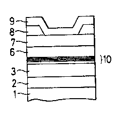
Fig. 1(a) shows the laser diode as one of the
embodiments of the present invention claimed in Claim 1.
Fig. 1(b) shows zero-bias energy band diagram of the laser
diode.
The laser diode shown in Figs. 1(a), (b) is made by
depositing an n-InP clad layer 2, a GaInAsp active layer 3,
a strained super lattice MQB layer 10 made of InP and 1~
tensile strained AlXIn1 XAs (x = 0.62), a p-InP clad layer 6,
a p-GaInAsP contact layer 7, an N-InP block layer 8 and p-
electrode 9 in the order of mention on an n-InP
13
x_ . , ~ CA 02055208 2000-04-07
substrate. Strained MQB layer 10 is p-doped up to about
1016 - 101' cm 3 .
Fig. 2 shows a potential configuration of a barrier
comprising InP a:nd AlX:In1 xAs (x = 0 . 62 ) involving in-plane
tensile strain of 1%. In this example, barrier layer is
provided between the p-InP clad layer 6 and GaInAsP active
layer 3.
The potential configuration in Fig. 2 has barrier
height of 510 meV against p-InP clad.
Therefore, 'when this strained barrier potential is
applied to 1.3 ,u m laser diodes, a practical-value of
maximum coefficient Rm~,X can be obtained, because Eo/Vo = 1.37
for the hot electrons incident with a maximum energy of 950
meV and corresponding RmaX value is 0.33 as is shown in Fig.
7 (b) .
That is such a strained super lattice barriers can have
maximum reflection coefficient of about 30% per barrier
layer. They can therefore be given a reflection coefficient
of 100% by integrating a number of such strained barrier
layers.
Fig. 3(a) shows the DCC laser diode as one of the other
embodiments of t:he present invention claimed in Claim 2, 3.
Fig. 3(b) shows its energy band diagram.
The laser diode in Figs. 3(a), (b) is fabricated by
depositing a 600,A-thick first GaInAsP active layer 3, a
14
CA 02055208 2000-04-07
0
strained super lattice MQB layer 10, a 400A-thick p-InP
0
middle clad layer 4, a 600A-thick second GaInAsP active
layer 5, a strained super lattice MQB layer 12, a p-InP clad
layer 6, a p-GaI:nAsP contact layer 7, an n-InP block layer 8
and p-electrode 9 in the order of mention on the n-InP clad
layer on an n-In:P substrate. The both active layers 3, 5
have same band g.ap wavelength A, value of 1.3 ~ m.
As described above, in conventional DCC structures,
characteristic temperature degrades and approaches to the
value of conventional laser diode when thickness of the
0
middle clad layer is reduced from 1,OOOA.
In the case of the DCC laser diode in Fig. 3(a), (b),
on the other hand, the hot electrons generated in the first
active layer 3 are reflected by the MQB layer 10 and the
electrons going to travel through to the p-clad layer 6,
maintaining a high energy, can be reflected by the MQB layer
12 and captured :by the second active layer 5.
The DCC laser devices in Fig. 3(a), (b), therefore,
permit thickness of middle clad layer 6 to be reduced to
small values and threshold current to be decreased
maintaining superior temperature characteristic.
Concerning material for the tensile strained super
lattice layers, GaIn(As)P barrier layer with a tensile
strain of about +5% can be also adopted as well as AlInAs
barrier with l~ tensilestrain: And as to active layer
structure, quantum welt (QW) structure accompanied by
suitable SCH (Separated Confinement Heterostructure) layer
can be used and realize lower threshold current density.
Regarding current blocking structure, BH (Burried Hetero
structure) or BC (BUrried Crescent) structures can be used
instead of the structure in Fig. l and 3.
In above embodiment, only semiconductor laser diodes
were described, but similar effect or improvement can be
expected as for semiconductor laser amplifier.
Effects of the Invention:
As is apparent from what is described heretofore, the
quantum barrier semiconductor optical devices according to
the invention produces such effects to be stated below.
One thereof is that we can realize an MQB layer with
the effective reflecting function for the hot electrons
generated due to Auger process. As a result, overflow
leakage current due to Auger process can be well supressed;
temperature characteristics can be drastically improved in
optical devices like LDs in longwavelength region.
Another thereof is that a low threshold current DCC
laser diode is obtainable.
BRLEF DESCRIPTION OF DRAWINGS
Fig. 1(a) is a cross sectional view of a Iongwavelength
region laser diode according to the present invention.
,,, , , ~, CA 02055208 2000-04-07
Fig. 1(b) shows its energy band diagram at zero-bias
condition.
Fig. 2 shows the energy band diagram of a strained
super lattice barrier between active layer and p-clad layer
in 1.3 ~ m LD, and the energy level of Auger electrons with
maximum incident energy. The barrier consists of an AlInAs
layer with 1% of in-plane tensile strain and InP layer.
Fig. 3(a) is a cross sectional view of a DCC laser
diode according to an embodiment of the present invention.
Fig. 3(b) shows its energy band diagram at zero-bias
condition.
Fig. 4(a) is a cross sectional view of a conventional
DCC laser diode. Fig. 4(b) shows its energy band diagram.
Fig. 4(c) shows its temperature characteristic.
Fig. 5 shows increase of effective hetero-barriers in
MQB structure.
Fig. 6(a) shows a one-dimensional square well potential
and Fig. 6(b) shows a one-dimensional square barrier
potential.
Fig. 7(a) shows the calculated results for the
dependence of maximum reflection coefficient on the ratio
(Eo/Vo) of the incidence energy and the depth of the well
for the square well potential in Fig. 6(a). Fig. 7(b) shows
the calculated results for the dependence of maximum
reflection coefficient on the ratio (Eo/Vo) of the
17
~o~~~os
incidence energy and the height of the barrier for the
square barrier potential in Fig. 6(b).
Fig. 8 shows the energy band diagram of a lattice
matched barrier between active layer and p-clad layer in
1.3 a m LD and the energy level of Auger electrons with
maximum incident energy. The barrier consists of lattice
matched AIInAs and InP.