Note: Descriptions are shown in the official language in which they were submitted.
,~ q ~ L 3 ; i ~>
-- 1 --
TITLE OF T~ INVENTION
LIGHT-EMITTING DIODE FOR CONCURRENTLY EMITTING
LIGHTS HAVING DIFFERENT WAVELENGTHS
BACRGROUND OF 1~ INVENTION
Field of the Invention
The present invention relates to a light-emitting
diode which is capable of concurrently emitting lights
having different wavelengths.
Discussion of the Prior Art
Light-emitting diodes (LED) are known as a
semiconductor diode consisting of a plurality of various
compound semiconductor layers which are superposed on a
semiconductor substrate by epitaxy, such as vapor phase
epitaxy or liquid phase epita~y, so as to form a pn
junction. It is proposed to provide the light-emitting diode
with two pn junctions, for example, so that the diode can
emit two kinds of lights having different wavelengths. An
example of such a light-emitting diode is disclosed on page
117 of "Compound Semiconductor Device II" (published on Jan.
10, 1986 from Kogyo Chosakai Publishing Co., Ltd., Tokyo,
Japan). The disclosed light-emitting diode is able to emit
two kinds of lights having different wavelengths at the same
time.
In fabricating the above-described diode having a
plurality of pn junctions for emitting different wavelengths
of lights, the number of at least the positive electrodes or
: ': '' ~ :.
:; ~
-- 2 --
at least the negative electrodes must be equal to the number
of the pn junctions, for applying drive currents to the
respective pn junctions. The provision of the increased
number of electrodes as well as the plurality of pn
junctions makes the fabricating process rather complicated,
and pushes up the cost of manufacture of the diode.
SUMMARY OF THE INVENTION
It is therefore an object of the present invention
to provide a light-emitting diode which is capable of
emitting two or more lights having different wavelengths at
the same time, and which can be fabricated in a
comparatively simple process.
The above object may be attained according to the
principle of the present invention, which provides a
light-emitting diode including a substrate and a plurality
of semiconductor layers superposed on the substrate, for
emitting at a time a plurality of lights having respective
di~ferent wavelengths, the plurality of lights being emitted
through a light-emitting surface, the plurality of
semiconductor layers comprising: ~a) an active layer for
generating a first light, upon application of an electric
current thereto; and (b) a plurality of photoluminescent
layers each for generating a light having a longer
wavelength than the first light, based on the first light
generated by the active layer.
, . ~ . : '
- ' . . :
- . .. . .
.
J~'~?~
-- 3
In the light-emitting diode constructed as
described above, when the first light is generated by the
active layer upon application of a current thereto, the
photoluminescent layer utilizes the first light so as to
generate the second light having a longer wavelength than
the first light. Thus, the present light-emitting diode can
generate a plurality of kinds of lights having different
wavelengths at the same time. In this arrangement, it is not
necessary to provide two or more p-n junctions and increase
1o the num~er of electrodes, so as to permit the diode to
generate two or more kinds of lights having different
wavelengths at the same time. Therefore, the process for
manufacturing the present light-emitting diode is
simplified, whereby the diode is available at a relatively
low cost.
BRIEF DESCRIPTION OF THE DRAWINGS
The above and optional objects, features and
advantages of the present invention will be better
understood by reading the following detailed description of
a presently preferred embodiment of the invention, when
considered in connection with the accompanying drawings, in
which:
Fig. 1 is a perspective view of one embodiment of
a light-emitting diode of the present invention;
Fig. 2 is an elevational view partly in cross
section of the light-emitting diode of Fig. l; and
,. ,;.
-- 4
Fig. 3 is a graph indicating a relative spectral
intensity of the light emitted by the diode of Fig. 1.
DETAILED DESCRIPTION OF T~E P~FERRED EMBODIMENT
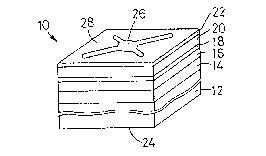
Referring to the perspective and elevational views
of Figs. 1 and 2, reference numeral 10 denotes a planar or
surface emission type light-emitting diode having a double-
heterostructure. The surface light-emitting diode 10 has a
p-GaAs single crystal substrate 12, a light-reflectingl
photoluminescent layer 14 grown on the substrate 12, a
p-GaO. 5 sAlo . 4 sAs clad layer 16 grown on the photoluminescent
layer 14, a p-GaO 87Alo l3As active layer 18 grown on the
clad layer 16, an n-GaO ssAlo 4 sAs clad layer 20 grown on
the active layer 18, and an n-GaAs contact layer 22 grown on
~he clad layer 20. The active layer 18 is adapted to
generate an electromagnetic light having a wavelength of
780nm by electroluminescence. The light-reflecting/
photoluminescent layer 14, clad layer 16, active layer 18,
clad layer 20 and contact layer 22 are sequentially grown
each as a single crystal on the substrate 12 in the order of
description, by metalorganic chemical vapor deposition
(MOCVD), for example. The substrate 12 has a thickness of
350~m, and the clad layers 16, 18 have a thickness of 2~m.
The active layer 18 and the contact layer 22 have a
thickness of 0.1~m. The light-emitting diode 10 has a square
shape in plane view having a top or bottom surEace area of
350~m x 350~m. On the surface of the p-semiconductor
. . . ........ .. .
. - : .
- 5
substrate 12 remote from the light-reflecting/
photoluminescent layer 14, there :is formed an n-AuGe/Ni/Au
ohmic electrode 24. The contact layer 22 has a
light-emitting surface 28 on which is formed a p-AuZn/Ti/Au
ohmic electrode 26.
The light-reflecting/photoluminescent layer 14
consists of a superlattice consisting of twenty films 30 of
p-AlAs each having a thickness of 65~m, and twenty films 32
of p-GaAs each having a thickness of 54~m. The p-AlAs films
30 and the p-GaAs films 32 are alternately superposed on
each other to fo~m the superlattice 14, which serves as a
wave interference type light reflector capable of reflecting
a component of the light generated by the active layer 18.
The layer 14 is also adapted to absorb a component of the
incident light generated by the active layer 18, and
generate a light having a wavelength of 87Onm, which is
longer than the wavelength (780nm) of the electromagnetic
light generated by the active layer 18. The light-
reflecting/photoluminescent layer 14 has p-GaAs films 32
whose energy gap is smaller than that of the active layer
18, which is represented by the energy of the light
generated by the active layer 18. In the instant embodiment,
the p-GaAs films 32 in the light-reflecting/photoluminescent
layer 14 also serve as a photoluminescent layer for
generating a second light (having a wavelength of 870nm),
based on a first light (having a wavelength of 780nm) which
is generated by the active layer 18. It is to be noted that
~,
-- 6 --
the thickness of the light-reflect:Lng/photoluminescent layer
14, clad layers 16, 20, active layer 18 and contact layer 22
as illustrated in Figs. 1 and 2 do not accurately represent
the actual thickness of these laye;rs 14, 16, 18, 20, 22.
In operation of the present light-emitting diode
10 constructed as described above, a drive current is
applied between the ohmic electrodes 26, 28 in the forward
direction, whereby the electromagnetic light having the
wavelength of 780nm is generated by the active layer 18. A
component of the light generated by the active layer 18 is
incident upon the contact layer 28 having the light-emitting
surface 28, and the incident component is emitted from the
light-emitting surface 22, externally of the diode 10, as
indicated in solid lines in Fig. 2. At the same time, a
component of the generated light is directed toward the
substrate 12 and is incident upon the light-reflecting/
photoluminescent layer 14. A portion of the incident
component is reflected by the layer 14 toward the active
layer 18, transmitted through the layer 18, and finally
emitted through the light-emitting surface 28, as indicated
in solid lines in Fig. 2. Another portion of the incident
component from the active layer 18 is absorbed by the
photoluminescent layer 14, whereby the light having the
wavelength of 870nm is generated by the layer 14,
transmitted through the active layer 18, and finally emitted
through the light-emitting surface 28, as indicated in the
broken lines in Fig. 2. In this manner, two kinds of lights
: . ,
- , :
- 7 - i'J ~
having different wavelengths are emitted at a time from the
light-emitting surface 28 of the diode 10. The graph of Fig.
3 indicates a relative spectral intensity of the light
emitted by the present light-emitting diode 10. The thus
constructed light-emitting diode 10 is used for optical
multiplex communication, or used as a light source for a
photosensor, for example.
In the instant em~odiment, the 780nm-wavelength
light and the 870nm-wavelength light are respectively
generated by the active layer 18 and the
light-reflecting/photoluminescent layer 14, only by applying
a drive current between one pair oE the ohmic electrodes 24,
26. Thus, the present light-emitting diode 10 is capable of
emitting two lights having di~ferent wavelengths at the same
time, b using only one pair of electrodes 24, 26. In this
arrangement, it is not necessary to provide two active
layers and increase the number of electrodes, so as to
permit the diode to concurrently generate two lights of
different wavelengths, as in the conventional light-emitting
diode. Thus, the process for fabricating the light-emitting
diode 10 is simplified, whereby the diode 10 is available at
a relatively low cost.
In the instant embodiment, the light-reflecting/
photoluminescent layer 14 is provided on the side of the
active layer 18 remote from the light-emitting surface 28.
Therefore, the component of the light generated by the
active layer 18 and directed toward the substrate 12 is
,f 3
-- 8
either reflected by the layer 14 so as to improve the
intensity of the 780nm-wavelength light emitted from the
light-emitting surface 28, or converted by the layer 14 into
the 870nm-wavelength light which is also emitted from the
light-emitting surface 28. Thus, the component of the light
incident upon the layer 14 is fully utilized for the optical
output of the diode 10, and the electric consumption by the
diode 10 is suitably reduced.
The AlAs/GaAs superlattice 30, 32 of the
light-reflecting/photoluminescent layer 14 does not suffer
from lattice mismatch with respect to the p-GaAs substrate
12 and the p-GaO 5 5Alo 4 5As clad layer 16.
While the present invention has been described in
the presently preferred embodiment with a certain degree of
particularity, for illustrative purpose only, it is to be
understood that the invention may be otherwise embodied.
Between the substrate 12 and the light-
reflecting/photoluminescent layer 14 of the illustrated
embodiment, there may be provided a light-reflecting layer
adapted to reflect a portion of the light generated by the
photoluminescent layer 14 toward the substrate 12, back
toward the light-emitting surface 28.
In the illustrated embodiment, the light-
reflecting/photoluminescent layer 14 is provided on the side
of the active layer 18 remote from the light-emitting
surface 28. However, the layer 14 may be replaced by a
light-transmitting photoluminescent layer. It is also
. , ,. . :
.: ., : . - :
:. , , . , ::,..~ :.
:
1" / .J' ~ "", .
possible to provide such a photoluminescent layer between
the active layer 18 and the light-emitting surface 28.
Alternatively, the light-reflecting photoluminescent layer
14 may be eliminated, and the substrate 12 or contact layer
22 may serve as a photoluminescent layer capable of emitting
a light which is different from the light generated by the
active layer 18.
In the illustrated embodiment, the light-emitting
diode 10 is adapted to emit two kinds of lights having
respective wavelengths of 780nm and 870nm at the same time.
However, the light-emitting diode of the invention may be
constructed so as to generate lights having wavelengths
other than 780nm and 870nm, by suitably selecting materials
for the active layer and the photoluminescent layer. It is
also possible to provide two or more photoluminescent layers
for generating at a time at least three kinds of lights
having different wavelengths. Where the diode is provided
with two or more photoluminescent layers, all these layers
may be adapted to absorb the light generated by the active
layer, so as to generate respective lights of different
wavelengths. Alternatively, one of the two or more
photoluminescent layers may absorb the light generated by
the active layer and generate a light having a different
wavelength, based on which another photoluminescent layer
generates a light having a further different wavelength. In
essence, the photoluminescent layer of the invention is
. . .
- , . : : . ,,
~i ~, : ... ., , "
,
c 1 ? ;
-- 10 --
required to generate at least one light, based on the first
light generated by the active layer.
While the diode lO of the illustrated embodiment
is a surface emission ~ype light-emitting diode having a
s GaAlAs double-heterostructure, other compound semiconductors
such as GaAs, GaP, InP, InGaAsP may be utilized to
constitute a double-heterostructure, a single-
heterostructure or a homostructure. Further, the present
invention is applicable to a diode of a type in which light
is emitted from an end face of the active layer. In this
case, a light having a wavelength different rom that of the
light generated by the active layer is emitted from an end
face of each photoluminescent layer provided at a desired
position.
It is to be understood that the present invention
may be embodied with various other changes, modifications
and improvements, which may occur to those s~illed in the
art, without departing from the spirit and scope of the
invention defined in the following claims.
.. i, :.. .. , :
.~.. ',: ' ~ . . ` '