Note: Descriptions are shown in the official language in which they were submitted.
~O~fi~~
a4Z13698-US
HIGH PIXEL APERTURE RATIO LIQUID CRYSTAL DISPLAY
Field of the Invention
The present invention pertains to displays,
and particularly, to liquid crystal displays (LCD's).
More particularly, the invention pertains to active
matrix LCD's having half tone gray scales and high
pixel aperture ratios.
Background of the Invention
LCD technology is being developed as a
possible successor to cathode rate (CRT) technology for
many applications. LCD technology offers important
advantages, such as higher reliability and reduced
power, size and weight. However, in the current state
of development, LCD image rendering capability falls
short of that achievable from the use of CRT's . The
present invention addresses one of the major technical
obstacles which involves viewing angle and brightness
limitations associated with LCD's when they are
operated in a gray scale mode.
~g~na~y of the Invention
The invention implements a half-tone gray
scale in the active matrix liquid crystal display
(AMLCD). As an example of the related art, gray scale
display technology incorporates four subpixels. There
is space between the subpixels which is inactive and
CA 02056293 2001-02-28
64159-1222
2
thus reduces the pixel aperture ratio. In the gray scale or
halftone pixel of the present invention, the entire pixel is
optically active due to the control capacitor array design of
the invention. The invention may incorporate a halftone pixel
with subpixels having uniform cell spacing or a halftone pixel
having concentric subpixels of different sizes.
In accordance with the present invention, there is
provided a halftone grayscale liquid crystal display comprising
a plurality of pixels having high pixel aperture ratio, wherein
each pixel comprises: a first substrate; an N number of
subpixels wherein each of N-1 subpixels comprises: a first
electrode on said first substrate; a layer of dielectric on
said first electrode; a second electrode on said layer of
dielectric; a layer of liquid crystal on said second electrode;
and a third electrode on said layer of liquid crystal; and
wherein the Nth subpixel comprises: a first electrode on said
first substrate; a layer of dielectric on said first electrode;
a layer of liquid crystal on said layer of dielectric; and a
second electrode on said layer of liquid crystal; and a second
substrate on said layer of liquid crystal; and wherein said
first electrodes of the N-1 subpixels are interconnected.
In accordance with the present invention, there is
further provided a halftone grayscale liquid crystal display
comprising a plurality of pixels having a high pixel aperture
ratio, wherein each pixel comprises: first, second, third,
fourth and fifth subpixels; a first glass substrate; a first
electrode on said glass substrate; a second electrode on said
glass substrate; a third electrode on said glass substrate; a
fourth electrode on said glass substrate; a fifth electrode
situated between said first, second, third and fourth
electrodes, respectively, on said glass substrate and proximate
to said fifth subpixel; a dielectric layer on said at least
first, second, third and fourth electrodes; a sixth electrode
CA 02056293 2001-02-28
64159-1222
2a
situated on said dielectric layer proximate to said first
electrode and said first subpixel; a seventh electrode situated
on said dielectric layer proximate to said second electrode and
said second subpixel; an eighth electrode situated on said
dielectric layer proximate to said third electrode and said
third subpixel; a ninth electrode situated on said dielectric
layer proximate to said fourth electrode and said fourth
subpixel; a liquid crystal layer situated on said fifth, sixth,
seventh, eighth and ninth electrodes; a tenth electrode on said
liquid crystal; and a second glass substrate on said tenth
electrode.
Brief Description of the Drawings
Figure 1 shows a layout of a halftone pixel according
to the related art.
1S Figures 2a and 2b show a layout and the electrical
equivalence of the related art halftone pixel.
Figure 3 shows a halftone pixel according to the
invention.
Figures 4a and 4b reveal a layout and the electrical
equivalent of the halftone pixel of the invention.
Figures 5a, 5b and 5c show a layout of the halftone
pixel for uniform cell spacing.
Figures 6a, 6b and 6c reveal a layout of a halftone
pixel having three concentric subpixels.
Figures 7a, 7b and 7c show a layout of a concentric-
type halftone pixel having a coupling capacitor.
~ r.. ~9 Cl c
-3-
Figure 8 illustrates a cross-section of a
display incorporating the half tone pixel configuration
of Figure 5.
pescript~on of the Preferred Embodiments
The present invention incorporates a half-tone
approach to the active matrix liquid crystal displays,
which is based on the fact that the liquid crystal
electro-optic response is essentially independent of
the viewing angle when it is operated in a bi-level
mode, i.e., either fully on or fully off. A control
capacitor approach has been developed to achieve the
half-tone gray scale. Such approach involves
subdividing the pixel into a number of subpixels, and
incorporating a control capacitor in series with each
subpixel. Figure 1 shows a layout of a half-tone pixel
12 having four subpixels 14, 16, I8 and 20. Space 22,
which is the shaded area between subpixels 14, 16, 18
and 20, is inactive and thus reduces the pixel aperture
ratio. Figure 2a reveals greater detail of the
construction of the half-tone pixel of Figure 1..
Figure 2b is a schematic of the electrical equivalent
w of the pixel illustrated in Figure 2a. Control
capacitors 2?, 29 and 31 act as voltage dividers and
serve to control the voltage across the liquid crystal
subpixels 14, 16, 18 and 20 thereby controlling the
number of subpixels that turn on as the source voltage
(Vs) of thin film transistor (TFT) 32 is changed to
~t~~~~~e>
- 4 -
vary the overall gray level of pixel 12. One or more
subpixels are either totally on or off. The control
capacitor values are determined so that at the most
only one subpixel is at a voltage between the threshold
and saturation voltages of the liquid crystal to
minimize the gray scale errors at off-normal viewing
angles. This approach improves the viewing angle
behavior of the AMLCD~s.
Control capacitors 27, 29 and 31 are
fabricated either on the active matrix substrate or on
the common electrode substrate. The capacitance for
each of the control capacitors 27, 29 and 31 is
determined according to the area far each of the
electrodes of these capacitors. A first layer of
indium tin oxide (ITO) 33 which is a transparent and
conducting oxide, defines the area of control
capacitors 27, 29 and 31. A dielectric film having a
controlled thickness, such as silicon nitride or
silicon dioxide, serves as the control capacitor
dielectric. There is a via 34 in the dielectric so as
to eliminate a control capacitor for subpixel 14. A
~-s~cond layer of ITO provides the electrodes of
subpixels 14, 16, 18 and 20. Capacitors 24, 26, 28 and
30 represent the incidental liquid crystal display
capacitances of subpixels 14, 16, 18 and 20,
respectively. Control capacitors 27, 29 and 31 are in
r
- 5 -
series with display capacitances 26, 28 and 30,
respectively.
A significant problem of the above-mentioned
approach is the reduction of pixel aperture ratio
(pixel luminance) which reduces the maximum brightness
and contrast achievable in the liquid crystal display.
Pixel aperture ratio is the sum of the active subpixel
areas divided by the total pixel area incorporating the
subpixels. The reduction of pixel aperture ratio is
due to space 36 between or among subpixels 14, 16, 18
and 20, not being optically active. To increase the
aperture ratio, space 36 among the subpixels 14, 16, 18
and 20, is reduced. However, product yield
considerations prevent the minimizing of intra-subpixel
spacing 36 and thus reducing the aperture ratio loss to
satisfactory levels. Further, optically inactive space
36 mandates the use of either a dark matrix between or
among subpixels 14, 16, 18 and 20 or a normally dark
mode of the AMLCD operation having parallel polarizers.
The use of the dark matrix between subpixels 14, 16, 18
and 20, increases the complexity of fabrication of a
~~dolor filter ray circuit due to the reduction in
feature sizes. Alternatively, a lack of normally white
mode of the AMLCD panel operation reduces design
flexibility and makes optimization for improved image
quality impractical. The present invention
~~~~~~%~~~:j
- 6 -
incorporating a new half-tone pixel design eliminates
these deficiencies and obstacles.
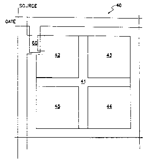
Figure 3 shows a drawing of a half-tone pixel
array according to the invention, having subpixels 41,
42, 43, 44 and 45. Figure 4a shows more detail of half
tone pixel 40 of Figure 3. Figure 4b is a schematic of
the electrical equivalent of half-tone pixel 40 of
Figure 4a. First ITO layer 46 defines areas for
control capacitors 62, 63, 64 and 65. Layer 48
represents the capacitor dielectric. Second ITO layer
50 defines the regions of subpixels 42, 43, 44 and 45.
In addition to defining the control capacitor areas,
the first ITO layer 46 defines the area of subpixel 41
which is the space between subpixels 42, 43, 44 and 45.
Cross-hatched area 48 represents a via and serves to
remove the series control capacitor for subpixel 41.
Because ITO layers 46 and 50 are separated by
dielectric layer 48, layers 46 and 50 can have a slight
overlap as shown in Figure 4a. Thus, in this design,
there are no restrictions with respect to minimum
subpixel spacing due to photolithographic processes, as
iri related art designs. The fabrication sequence of
the control capacitor array of Figure 4 is: 1) deposit,
pattern and etch first ITO layer 46, 2) deposit control
capacitor dielectric 48, 3) deposit, pattern and etch
second ITO layer 50, and 4) pattern and etch a via in
dielectric 48 to~define subpixel 41.
~~~ ~~~=qrj
_7_
The design of half-tone pixel 40 results in
100 percent of the pixel being optically active. As a
result, such design allows implementation of half-tone
gray scale using a control capacitor approach with no
reductions in the maximum pixel aperture ratio,
brightness, and contrast.
A feature of the half-tone pixel 40 design of
Figures 4a and 4b is that the layout of layers 46, 48
and 50 are such that subpixel 41, having no series
control capacitor, is positioned at the intro-subpixel
region.
Even though Figures 3, 4a and 4b show five
subpixels, any number of subpixels may be utilized with
the present invention. Since entire pixel 40 is
optically active, there is additional flexibility for
various subpixel layouts and subpixel turn-on sequences
for desired image quality.
Figures 5a, 5b and 5c reveal another layout of
a half-tone pixel 70. Figure 5a shows a six subpixel
design having subpixels 71, 72, 73, 74, 75 and 76.
Layer 78 is continuous throughout the pixel except for
- ~~a~small contact via 80 at the subpixel 71 region as
illustrated in Figures 5a and 5b. The continuity of
layer 78 permits the entire liquid crystal cell or
pixel 70 except for the small contact via region 80, to
be maintained at the Gooch-Tarry minimum cell spacing,
for maximum contrast. Gooch and Tarry derived an
~~~~ Vita
_8_
optimum value for liquid crystal cell spacing that
would result in the best off-state and thus at a
maximum contrast. Layers 81 and 82 of ITO are revealed
in Figure 5a. The layout of layers 81, 78 and 82 are
such that subpixel 71, whose area is defined by ITO
layer 81, is positioned at the intra-subpixel region.
Figures 6a, 6b and 6c show the layout of a
half-tone pixel 90 having three concentric subpixels
91, 92 and 93. Figure 6c shows the electrical
equivalent of pixel 90. Layer 96 is continuous in
pixel 90 except for small contact via region 100. ITO
layers 94 and 98 delineate the control capacitor and
subpixel areas, respectively.
Figures 7a, 7b and 7c reveal another half-tone
subpixel arrangement. Figure 7a shows a halftone pixel
104 having three concentric subpixels 101, 102, and
103. Figure 7b is a cross sectional view of the
halftone pixel 104. Figure 7c is a schematic of the
electrical equivalent of pixel 104. It includes a
coupling capacitor, Cc, 106. The role of coupling
capacitor 106 is to provide additional flexibility in
~~t~ie choice of the dielectric materials used, and the
thicknesses employed, in the fabrication of control
capacitors C2 and Cg.
Figure 8 shows the cross-section for a display
employing the control capacitor design shown in Figures
5a-c. Control capacitor array 84 is fabricated along
with the TFT array 86 on the same substrate 88. The
drain electrode of the TFT 86 is connected to first ITO
electrode 81 defining the control capacitor areas of
array 84. After active matrix substrate 88 with
control capacitor array 84 is fabricated, display
assembly 110 is fabricated by sandwiching liquid
crystal 112 between active matrix substrate 88 and
common electrade substrate 114, using conventional
liquid crystal display assembly technologies.