Note: Descriptions are shown in the official language in which they were submitted.
- 20~G737
VIA RESISTORS WITHIN MULTI-LAYER, 3-DIMENSIONAL
STRUCTURES/SUBSTRATES
BACKGROUND OF THE INVENTION
The disclosed invention is directed generally to
hybrid multilayer circuit structures, and is directed more
particularly to hybrid multilayer circuit structures having
resistors formed in the vias thereof.
Hybrid multilayer circuit structures, also known as
hybrid microcircuits, implement the interconnection and
packaging of discrete circuit devices, and generally
include a unitized multilayer circuit structure formed from
a plurality of integrally fused insulating layers (e.g.,
ceramic layers) having conductor traces disposed therebe-
tween. The discrete circuit devices (e.g., integrated
circuits) are commonly mounted on the top insulating layer
so as not to be covered by another insulating layer or on
a insulating layer having die cutouts formed thereon to
provide cavities for the discrete devices. Passive compo-
nents such as capacitors and resistors can be formed on the
same layer that supports the discrete devices, for example,
by thick film processes, or they can be formed between the
insulating layers, for example, also by thick film process-
es. Electrical interconnection of the conductors and
components on the different layers is achieved with vias or
holes appropriately located and formed in the insulating
layers and filled with conductive via fill material,
2056737
whereby the conductive material is in contact with prede-
termined conductive traces between the layers that extend
over or under the vias.
The traditional thick film process for making resis-
tors involves screen printing of resistive ink in a hori-
zontal pattern where length, width and thickness are
controlled to define resistance value.
A consideration with screen printed resistors is the
difficulty in controlling their values, and the requirement
for precision capacitors is met by mounting discrete
capacitors on the top insulating layer along with other
discrete devices, and/or by forming screen printed resis-
tors on the top layer which are trimmed, for example, by
laser or abrasive trimming. The requirement for precision
capacitors has also been met by formation and trimming of
buried screen printed resistors, as disclosed in commonly
assigned U.S. Patent 4,792,779.
A further consideration with screen printed resistors
as well as discrete resistors is the substrate area uti-
lized by such components.
SUMMARY OF THE INVENTION
It would therefore be an advantage to provide for
resistors for multilayer hybrid circuits having reduced
substrate space requirements.
Another advantage would be to provide for resistors
for multilayer hybrid circuits having precisely controlla-
ble values as well as precisely controllable ratios.
The foregoing and other advantages are provided by the
invention in via resistor structures implemented in a
unitized multilayer circuit having a plurality of insulat-
ing layers. A disclosed via resistor structure includes a
plurality of resistive via fills in vias in respective
adjacent insulating layers, a plurality of conductive
_ 3 20567~7
elements for electrically contacting predetermined tops
and bottoms of the resistive via fills, and conductive via
fills for providing external electrical connection to
selected ones of the conductive elements at locations on
the outside the unitized multilayer circuit structure. A
further via resistor structure includes a resistive via
fill formed in a via in one of the insulating layers, and
one or more thermally conductive via fills for thermally
conducting heat from said resistive via fill to the
outside of the unitized multilayer circuit structure.
Another via resistor structure comprises ratioed via
resistors comprising a plurality of resistive via fills
formed in respective vias in one of the insulating layers,
said vias having substantially the same thickness and
having respective cross-sectional areas selected to
provide resistance values having predetermined ratios.
Other aspects of this invention are as follows:
A resistor structure in a cofired unitized multilayer
circuit structure having a plurality of insulating layers
formed of insulating tape, comprising:
a plurality of resistive via fills in vias in
respective adjacent insulating layers forming respective
via resistors having precisely controlled resistance
values;
a plurality of conductive means for electrically
contacting predetermined tops and bottoms of the resistive
via fills; and
electrical connection means for providing external
electrical connection to selected ones of said conductive
means at locations on the outside the unitized multilayer
circuit structure.
A resistor structure in a cofired unitized multilayer
circuit structure having a plurality of insulating layers
formed of insulating tape, comprising:
_ 3a 2056737
a resistive via fill formed in a via in one of the
insulating layers and forming a via resistor having a
precisely controlled resistance value; and
5one or more thermally conductive via fills for
thermally conducting heat from said resistive via fill to
the outside of the unitized multilayer circuit structure.
A resistor structure in a cofired unitized multilayer
circuit structure having a plurality of insulating layers
10formed of insulating tape, comprising:
a plurality of resistive via fills comprising the
same via fill material formed in respective vias in one of
the insulating layers, said vias having substantially the
same thickness and having respective cross-sectional areas
15selected to provide resistance values having predetermined
precisely controlled ratios; and
contact means electrically connected to the tops and
bottoms of said plurality of resistive via fills.
BRIEF DESCRIPTION OF THE DRAWINGS
20The advantages and features of the disclosed
invention will be readily appreciated by persons skilled
in the art from the following detailed description when
read in conjunction with the drawing wherein:
FIGS. 1 through 4 are schematic sectional views of
25illustrative examples of via resistor structures in
accordance with the invention.
FIGS. 5 and 6 are circuit schematics of the via
resistor structures respectively illustrated in FIG. 1 and
FIGS. 2A, 2B.
30DETAILED DESCRIPTION OF THE DISCLOSURE
In the following detailed description and in the
several figures of the drawing, like elements are
identified with like reference numerals.
~. .,--~
2056737
Via resistor structures in accordance with the inven-
tion are implemented in a unitized multilayer circuit
structure that is utilized for interconnecting various
discrete circuits mounted on the outside of the unitized
structure. The unitized multilayer circuit structure is
formed from a plurality of insulating layers (comprising
ceramic, for example), conductive traces disposed between
the layers, and conductive vias formed in the layers which
together with any buried elements (e.g., elements formed on
the top of an insulating layer and covered by an overlying
insulating layer) are processed to form an integrally fused
unitized multilayer structure. The discrete circuits are
typically mounted and electrically connected on the outside
of the unitized multilayer circuit structure after the
unitizing fabrication.
FIGS. 1 through 4 schematically depict the implementa-
tion of illustrative examples of via resistor structures in
accordance with the invention. Each via resistor includes
a resistive via fill, a first electrically conductive
element in contact with the top of the resistive via fill,
and a second electrically conductive element in electrical
contact with the resistive via fill. Each of the electri-
cally conductive elements can comprise a conductive trace,
a conductive via fill, or an external contact connection
such as a conductive epoxy connection.
In the following description, the different elements
of the via resistor structures will be referenced as
follows. Conductor traces are identified by reference
numerals in the form of lOXY, wherein X is the layer number
on which the trace is formed (for example, pursuant to
single side printing on the top side of each insulating
layer) and Y is the particular resistor structure A, B, C,
or D. Resistive via fills are identified by reference
numerals in the form of 20XY, wherein X is the layer number
in which the via fill is formed and Y is the particular
20~S7~37
resistor structure A, B, C, or D. Standard electrically
conductive via fills are identified by reference numerals
in the form of 30XY, 40XY, 50XY, 60XY wherein X is the
layer number in which the via fill is formed and Y is the
particular resistor structure A, B, C, or D. Thermally
conductive via fills are identified by the reference
numerals in the form of 90XY wherein X is the layer number
in which the via fill is formed and Y is the particular
resistor structure A, B, C, or D. To avoid ambiguity, the
thermally conductive via fills are explicitly referenced
with the terms "thermally" or "thermal".
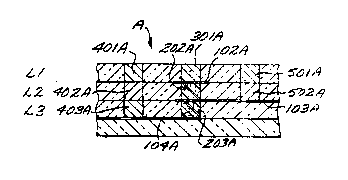
FIG. 1 illustrates a stacked via resistor structure A
that includes a resistive via fill 202A formed in a via in
the layer L2 and a resistive via fill 203A formed in a via
in the layer L2. A conductive trace 102A overlies the
resistive via fill 202A, a conductive trace 103A underlies
the resistive via fill 202A and overlies the resistive via
fill 203A, and a conductive trace 104A underlies the
resistive via fill 203A. A conductive via fill 301A
overlies the conductive trace 102A and extends to the
outside of the unitized multilayer structure and is avail-
able for external electrical connection. It should be
appreciated that the conductive trace 102A can be eliminat-
ed if it is not necessary for the particular application,
in which case the conductive via fill 301A would directly
contact the resistive via fill 202A .
Standard conductive via fills 401A, 402A, 403A are
electrically connected to the conductive trace 104A to
provide electrical access to the conductive trace by
external connection to the conductive via fill 401A which
extends to the outside of the unitized multilayer circuit
structure and is available for external connection.
Standard conductive via fills 501A, 502A are electrically
connected to the conductive trace 103A to provide electri-
cal access to the conductive trace by external connection
20~737
to the conductive via fill 501A which extends to the
outside of the unitized multilayer circuit structure and is
available for external connection. Effectively, the
conductive vias electrically connect the resistors to the
outside of the unitized multilayer circuit structure where
external connections can be made.
By appropriate internal connections of conductor
traces and/or external connections, the resistors in the
resistor structure A can be connected in parallel or serial
configurations, or they can be individually shorted.
An equivalent circuit of the via resistor structure A
is shown in FIG. 5, with the terminals of the resistors
identified by the reference numerals of the conductive via
fills that are available for external electrical connection
on the outside of the unitized multilayer circuit struc-
ture. Connection of the conductive via fill 401A to the
conductive via fill 301A, for example, by wire bonding,
connects the resistors Al and A2 in parallel. Connecting
the conductive via fill 301A to the conductive via fill
501A shorts the resistor Al.
FIGS. 2A and 2B illustrate a stacked via resistor
structure B that includes a resistive via fill 201B formed
in a via in the layer Ll, a resistive via fill 202B formed
in the layer L2, and a resistive via fill 203B formed in
2 5 the layer L3. The resistor structure further includes a
conductor trace lOlB that overlies the resistor via fill
201B, a conductor trace 102B that underlies the resistive
via fill 201B and overlies the resistive via fill 202B, a
conductor trace 103B that underlies the resistive via fill
202B and overlies the resistive via fill 203B, and a
conductive trace 104B that underlies the resistive via fill
203B. It should be appreciated that another contact such
as a conductive epoxy connection can be substituted for the
conductor trace lOlB.
2056737
Standard conductive via fills 401B, 402B, 403B are
electrically connected to the conductive trace 104B to
provide electrical access to the conductive trace by
external connection to the conductive via fill 401B which
extends to the outside of the unitized multilayer circuit
structure and is available for external electrical connec-
tion. Standard conductive via fills 501B, 502B are elec-
trically connected to the conductive trace 103B to provide
electrical access to the conductive trace by external
electrical connection to the conductive via fill 501B which
extends to the outside of the unitized multilayer circuit
structure and is available for external electrical connec-
tion.
By appropriate internal connections of conductor
traces and/or external connections, the resistors in the
resistor structure B can be connected in parallel or serial
configurations, or they can be individually shorted.
An equivalent circuit of the via resistor structure B
is shown in FIG. 6, with the terminals of the resistors
identified by the reference numerals of the conductor trace
lOlB and the conductive via fills that are available for
physical external connections on the outside of the unit-
ized multilayer circuit structure. External connection of
the conductive via fill 501B to the conductive trace lOlB
connects the resistors Bl and B2 in parallel. External
connection of the conductive trace lOlB to the conductive
via fill 601B shorts the resistor Bl. External connection
of the conductive via fill 401B to the conductive via fill
601B connects the resistors B2 and B3 in parallel. The
resistors can be configured in series by respective connec-
tions to the conductive trace lOlB and the conductive via
fill 401B without connections to the conductive via fills
501B, 601B.
For via resistor stacks having a larger number of via
resistors, the capability for external electrical connec-
8 2056737
tions on the outside of the unitized multilayer circuit
structure can be provided by respective axially aligned
conductive vias for selected buried conductive traces in
contact with the via resistors, wherein the conductive vias
for each selected buried trace extends upwardly from the
trace through the top layer Ll. By way of illustrative
example, the via structures comprising respective aligned
vias can be arranged in a circular pattern around the axis
of the aligned resistive via fills of the resistor struc-
ture, with each conductive via structure extending down-
wardly to a different layer, which would be an extension of
the externally accessible via structure of the resistor
structure of FIGS. 2A, 2B.
It should be appreciated that, depending on factors
affecting the electrical and thermal integrity of the
unitized multilayer circuit structure, the stacked resis-
tors of the via resistor structures A and B can be axially
aligned or staggered wherein via resistor fills in any two
adjacent layers are not axially aligned.
It should be also appreciated that laterally separated
via resistor structures in accordance with the invention
can be interconnected by external connections on the
outside of the unitized multilayer circuit structure, and
that interconnection can also be made by selectively
cutting conductive traces on the top layer that are formed
as part of the unitizing multilayer structure fabrication
so as to selectively sever electrical connections between
conductive via fills and/or resistor via fills. For
example, a plurality of via resistors could be connected in
a parallel circuit by conductive traces on the outside of
the unitized multilayer circuit structure, and selected
resistors could be removed from the circuit by cutting
appropriate conductor traces by laser cutting or abrasion,
for example.
9 2056737
While the foregoing has shown a via resistor structure
with resistive via fills in adjacent layers being separated
by intervening conductor traces, it should be appreciated
that via resistor structures in accordance with the inven-
tion can include a plurality of axially aligned stackedresistive via fills without intervening conductive traces.
In other words, the conductor traces are located as re-
quired to achieve the desired resistance values and inter-
connection capabilities.
Referring now to FIG. 3, set forth therein is a via
resistor structure C which includes a low thermal resis-
tance path for transferring thermal energy from the resis-
tor structure to the outside of the unitized multilayer
circuit structure in which the resistor structure is
implemented. The resistor structure C includes a resistor
via fill 203C, a conductive via 302C overlying the resistor
via fill 203C, and a conductive via fill 304C underlying
the resistor via fill 203C. A thermal via fill 901C, which
can comprise the same material as conductive via fills,
overlies the conductive via fill 302C. A plurality of
thermal via fills 905C, ... 90(N-l)C underlie the conduc-
tive via fill 304C. An electrical isolation layer L(N)
electrically isolates the lower most thermal via fill 90(N-
l)C from a heat sink 11. Appropriate conductive traces,
not shown, can be utilized for interconnection to the via
resistor formed by the resistive via- fill 203C. The
thermal via fills can also comprise metal matrix composite
inserts.
The thermal vias in combination with the electrically
conductive vias provide low thermal resistance paths to the
outside of the unitized multilayer circuit structure that
transfer heat from the via resistor so as to reduce the
temperature of the via resistor and the surrounding region.
It should be appreciated that although the via resistor
structure C includes two via thermal paths, a single
20~S~37
thermal path can also be utilized. Also, if heat sinking
is available on the top of the unitized multilayer circuit
structure, the top thermal via can be thermally connected
thereto through an electrically insulating layer.
The values of the via resistors in the via resistor
structures are controlled by (a) the cross-sectional area
of the filled vias, (b) the electrical characteristics of
the resistive via fill material, and/or (c) the number and
thicknesses of resistive via fills between the electrical
contacts of a resistor, wherein the thickness of a resis-
tive via fill is determined by the thickness of the insu-
lating layer in which it is formed.
Ratioed resistors (i.e., resistors whose values have
predetermined ratios relative to each other) are readily
made by appropriately varying the diameter of the vias for
the resistive via fills or utilizing resistive via fill
materials having different resistivities. Thus, for
example, for a given resistive via fill material and the
same via fill thickness, a via resistor having a resistive
via fill that has twice the cross-sectional area of another
resistor would have a resistance value that is one-half the
resistance value of such other resistor. As another
example, for a given resistive via fill material and the
same via cross-sectional area, a via resistor having twice
the thickness of another resistor would have a resistance
value of twice that of such other resistor.
Ratioing can also be achieved by appropriate connec-
tions of the resistors in a stacked resistor structure
wherein all via resistors in the stack have the same via
dimensions and the same resistive via fill material. For
example, two of such via resistors connected serially would
provide twice the resistance of one of the stacked resis-
tors, three of such via resistors connected serially would
provide three times the resistance of the one of the
stacked resistors, and so forth.
20~ ~ 37
Precisely ratioed resistors are advantageously provid-
ed with via resistors formed in the same layer and having
the same resistor via fill material and the same thickness.
Referring in particular to FIG. 4, schematically illustrat-
ed therein is a resistor structure D that includes aplurality of ratioed via resistors D1, D2, D3, D4 formed in
a layer L2 of a unitized multilayer circuit structure and
respectively comprising resistive via fills 202D1, 202D2,
202D3, 202D4. Electrical connections to the via resistor
are made by appropriate conductive traces and/or conductive
via fills as discussed and illustrated above. Also, each
of the resistors can be thermally conductively connected to
the outside of the unitized multilayer circuit by conduc-
tive and/or thermal vias as discussed above relative to
FIG. 3.
The via resistors D1, D2, D3, D4 are formed in same
layer of the same resistor via fill material and have the
same thicknesses. The ratioed values of the resistors are
controlled by the ratios of their cross-sectional areas.
For example, for circular cross-sections that decrease from
the resistor D1 to the resistor D4, the values of the
resistors can be made to increase by a factor of 2 by
controlling the via diameters to decrease by a factor of
1/(2)~ (i.e., the inverse of the square root of 2). In
particular, if the resistor D1 has a via diameter d and a
resistance value R, the resistor D2 would have a value of
2R by making its via diameter equal to d/(2)~. The resistor
D3 would have a value of 4R by making its via diameter
equal to d/[(2)%(2)%] (i.e., d/2). The resistor D4 would
have a value of 8R by making its via diameter equal to
d/[2(2)%]-
By way of illustrative example, the vias for ratioedresistors in the same layer can be accurately formed with
diamond tip mechanical punches whose diameters have been
20~6737
machined to high tolerances so as to precisely define the
ratios of the via resistors.
Examples of circuits that can be advantageously
implemented with via resistor structures in accordance with
the invention include voltage divider networks for generat-
ing reference voltages, digital-to-analog converter cir-
cuits, analog voltage summing circuits, and attenuator
circuits.
The conductive via fills can comprise standard conduc-
tive via fill material as traditionally utilized for
interconnections, and examples of commercially available
resistive via fill materials include DuPont l900TM Series
resistor inks, DuPont 4700TM Series resistor inks, DuPont
5900TM Series resistor inks, and Ferro 85-xxx~ Series resistor
inks. As indicated above, the thermal vias can comprise
standard conductive via fill material or metal matrix
composite inserts.
The resistor structures in accordance with the inven-
tion are made, for example, pursuant to low temperature co-
fired processing such as disclosed in "Development of a Low
Temperature Co-fired Multilayer Ceramic Technology," by
William A. Vitriol et al., 1983 ISHM Proceedings, pages
593-598; "Processing and Reliability of Resistors Incorpo-
rated Within Low Temperature Co-fired Ceramic Structures,"
by Ramona G. Pond et al., 1986 ISHM Proceedings, pages 461-
472; and "Low Temperature Co-Fireable Ceramics with Co-
Fired Resistors," by H. T. Sawhill et al., 1986 ISHM
Proceedings, pages 268-271.
In accordance with low temperature co-fired process-
ing, vias are formed in a plurality of green thick film
tape layers at locations defined by the desired via config-
urations of the desired multilayer circuit. The vias are
filled with the appropriate conductive and resistive fill
material, for example, by screen printing. Conductor
metallization for conductive traces including those that
13 2056737
contact the via resistors are then deposited on the indi-
vidual tape layers by screen printing, for example, and
materials for forming passive components are deposited on
the tape layers. The tape layers are laminated and fired
at a temperature below 1200 degrees Celsius (typically 850
degrees Celsius) for a predetermined length of time which
drives off organic materials contained in the green ceramic
tape and forms a solid ceramic substrate.
The foregoing has been a disclosure of a via resistor
structure for multilayer hybrid circuits which advanta-
geously utilizes vias to provide for increased circuit
packing density and which easily provides for precision and
ratioed resistors. The via resistor structure of the
invention further provides for resistor circuitry whose
connections can be modified after fabrication of the hybrid
in which they are implemented. The foregoing has also been
a disclosure of a via resistor structure that includes
thermally conductive paths for dissipating resistor heat.
Although the foregoing has been a description and
illustration of specific embodiments of the invention,
various modifications and changes thereto can be made by
persons skilled in the art without departing from the scope
and spirit of the invention as defined by the following
claims.