Note: Descriptions are shown in the official language in which they were submitted.
20~7717
0 44 1
PARALLEL INVERTER SYSTEM
BACKGROUND OF THE INVENTION
FIELD OF THE INVENTION:
The present invention relates to a power supply system
in which a plurality of AC output inverting devices like
inverters are connected and operated in parallel with respect
to common load, and more particularly to a means for
controlling the current balance between inverting devices for
use in the system.
DESCRIPTION OF THE RELATED ART:
Fig. 10 shows a schematic view of a parallel operational
system of a conventional AC output inverter disclosed in, for
example, Japanese Patent Publication Nos. 53-36137 and 56-
13101.
Referring to Fig. 10, a first inverter device 11
operates in parallel with a second inverter device 12, which
has like construction, through an output bus 13 and supplies
electric power to a load 14. The first inverter device 11 is
mainly composed of an inverter body 110, a reactor 111 and a
condenser 112 serving as a filter, inverts electric power of
a DC power supply 15 into AC power, and is connected to the
I output bus 13 through an output switch 113a. In order to
operate the first and second inverter devices 11 and 12 in
parallel, a detection signal I1a is obtained from an output
20~7717
current Il of the first inverter device 11 by a current
transformer (CT) 120a, and a difference between the detection
signal I1a and a detection signal I2a similarly obtained from
the second inverter device 12, that is, a signal ~Il
corresponding to cross current is obtained by a cross current
detector 151. Then, two orthogonal voltage vectors EA and EB
are generated by a phase shifter 150, and a reactive power
corresponding component ~Q and an active power corresponding
component ~P are obtained from the signal ~Il by arithmetic
circuits 152 and 153, respectively. A voltage control
circuit 143 performs pulse width modulation for the inverter
body 110 through a PWM circuit 140 based on signals from a
voltage setting circuit 17 and a voltage feedback circuit
130, thereby controlling the internal voltage.
The above reactive power corresponding component ~Q is
supplied as a supplementary signal to the voltage control
circuit 143, and the internal voltage of the inverter body
110 is adjusted by at most several percent so that ~Q becomes
0.
On the other hand, the active power corresponding
component ~P is input to a reference oscillator 155 through
an amplifier 154 as a component of a PLL circuit, and the
phase of the internal voltage of the inverter body 110 is
controlled by finely adjusting the frequency of the reference
oscillator 155 so that ~P becomes 0.
20S7717
-
Since the voltage and the phase are thus controlled so
that both ~Q and ~P become 0, no cross current exists between
the two inverters and stable load sharing is achieved.
However, the conventional parallel operational system of
inverters has the following three problems. First, since
shared currents are balanced by controlling the phase and an
average value of the internal voltages of the inverters, it
is difficult to improve the response speed of control, and,
in particular, it is impossible to control instantaneous
cross current. Secondly, since a filter is necessary to
detect an active component and a reactive component of the
cross current separately, the cross current cannot be
controlled at high speed. Therefore, there is a limit in
applying the system to high speed voltage control, for
example, instantaneous waveform control which keeps an output
of the inverter a sine wave of high quality with little
distortion. Thirdly, since the active component and the
reactive component of the cross current are separately
controlled, the control circuit is complicated.
SUMMARY OF THE INVENTION
Accordingly, an object of the present invention is to
provide a parallel inverter system capable of balancing
shared currents at high speed without separating the cross
current into an active component and a reactive component.
2057717
-
According to an aspect of the present invention, there
is provided a parallel inverter system which comprises a
plurality of AC output inverters of an instantaneous voltage
control type, a bus for connecting outputs of the plurality
of inverters to a load so as to share the load current, a
first detection means for detecting a cross current component
of a current flowing among the inverters, and a control means
for controlling the output voltages of the inverters so as to
suppress the cross current component detected by the first
detection means.
BRIEF DESCRIPTION OF THE DRAWINGS
Fig. 1 is a block diagram of a parallel inverter system
according to a first embodiment of the present invention;
Figs. 2A and 2B each are a circuit diagram of an
inverter for use in the present invention;
Fig. 3 is a block diagram of a current detection circuit
in the first embodiment;
Fig. 4 is a simplified block diagram of the system shown
in Fig. 1;
Fig. 5 is a circuit diagram of the current detection
clrcult;
Fig. 6 is a block diagram of a second embodiment;
Fig. 7 is a block diagram of a third embodiment;
Fig. 8 is a circuit diagram of another inverter for use
in the present invention;
2057717
Fig. 9 is a timing chart showing the operation of the
inverter shown in Fig. 8; and
Fig. 10 is a block diagram of a conventional parallel
operational system.
DESCRIPTION OF THE PREFERRED EMBODIMENTS
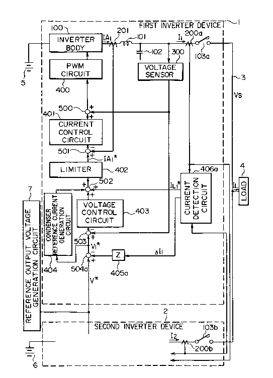
Referring to Fig. 1, a first inverter device 1 operates
in parallel with a second inverter device 2, which is briefly
illustrated and has the same construction, through an output
bus 3, and supplies electric power to a load 4. Numerals 5,
6 and 7 denote a DC power supply connected to the first
inverter device 1, a DC power supply connected to the second
inverter device 2, and a reference output voltage generation
circuit for generating a voltage command value for the output
bus 3.
Numerals after 100 denote components of the inverter
devices 1 and 2. The numerals with no subscript or with the
subscript "a" denote components of the first inverter device
1, and the numerals with the subscript "b" denote components
of the second inverter device 2.
An inverter body 100 is composed of self arc-suppressing
elements, for example, transistors or MOSFETs capable of
performing high frequency switching and may be a three-phase
bridge inverter shown in Fig. 2A or a single-phase bridge
inverter shown in Fig. 2B arms of which are switched at high
frequency of approximately ten or several hundreds of times
2057717
-
as high as an output frequency (for example, 60Hz), and
inverts DC voltage into high-frequency AC voltage in the
shape of a rectangular wave including a sine fundamental
wave. Numerals 101 and 102 denote a reactor and a condenser
constituting a low-pass filter, each of which removes
harmonics from the high-frequency AC voltage in the shape of
a rectangular wave generated by the inverter body 100,
obtains an output voltage in a sine wave, and is connected to
the output bus 3 through an output switch 103a.
Current detectors 200a and 201 detect an output current
I1 of the first inverter device 1 and an output current IA1 of
the inverter body 100, respectively. A voltage detector 300
detects a voltage of the condenser 102, that is, an output
bus voltage in the parallel operation of the inverter devices
1 and 2.
A PWM circuit 400 for determining the timing of
switching of the inverter body 100 is, for example, a
triangular wave comparison PWM circuit which makes the
inverter body 100 perform switching in response to the
crossing of a voltage command signal for a fundamental wave
to be output from the inverter body 100 and a triangular wave
carrier. A current control circuit 401 controls the output
current IA1 of the inverter body 100, a limiter circuit 402
limits an output current command value of the inverter body
100, and a voltage control circuit 403 controls the voltage
20S7717
of the condenser 102. A condenser reference current
generation circuit 404 outputs a current value to be supplied
to the condenser 102 in order to generate a desired output
voltage. A virtual impedance circuit 405a suppresses cross
current by virtually inserting an impedance Z between the
first and second inverter devices 1 and 2. A current
detection circuit 406a detects the cross current output from
the first inverter device 1 and a load current value to be
shared. Numerals 500, 501, 502, 503 and 504a denote adders
and subtracters.
The second inverter device 2 has the same construction
as that of the first inverter device 1, and the outputs of
the first and second inverter devices 1 and 2 are connected
in parallel through the output bus 3. Numerals 103b and 200b
denote an output switch of the second inverter device 2 and a
current sensor for detecting an output current I2 of the
second inverter device 2.
Fig. 3 is a detailed block diagram of the current
detection circuit 406a. Numerals 406s and 406t denote an
adder and a subtracter, respectively. Numeral 406u denotes
an amplifying circuit having a gain of 1/n when the number of
inverter devices disposed in parallel is n. A load current IL
is found by adding the output current I1 of the first inverter
device 1 and the output current I2 of the second inverter
device 2 in the adder 406s, and a value IL/n is calculated by
2057717
-
inputting a signal corresponding to the load current IL to the
amplifying circuit 406u to divide the load current IL by the
number of parallel inverters n (n = 2 in this embodiment),
and output as a load current IL1 * to be shared by the first
inverter device 1. Furthermore, a difference between the
output current Il of the first inverter device 1 and the
current IL1* to be shared, that is, a cross current ~Il (= I
~ IL1*) is calculated and output by the subtracter 406t.
Operations of the parallel inverter system will be now
described. Each of the inverter devices 1 and 2 is formed
with a current minor loop. The current control circuit 401
outputs a voltage to be applied to the reactor 101 so that an
output current IA1 of the inverter body 100 fed back by the
current sensor 201 agrees with a current command IA1* from the
limiter circuit 402. Since the condenser 102 and the voltage
caused by the second inverter device 2 are present on the
output bus 3, it is necessary that the inverter body 100
generates the total of the voltage of the output bus 3 and
the voltage to be applied to the reactor 101 in order to
apply a desired voltage to the reactor 101. Therefore, the
voltage of the condenser 102 detected by the voltage sensor
300 and the output of the current control circuit 401 are
~added by the adder 500 and supplied as a voltage command to
the PWM circuit 400.
20~7717
The condenser reference current generation circuit 404
generates a sine wave reference current signal as a current
to flow in the condenser 102, which is advanced by 90 from a
voltage command V1* of the condenser 102 in accordance with
the capacity of the condenser 102. The voltage command V1* of
the condenser 102 can be obtained by the output of the
subtracter 504a as described below. A deviation between the
voltage command V1* of the condenser 102 and the voltage of
the condenser 102 detected by the voltage sensor 300 is
calculated by the subtracter 503, and the voltage control
circuit 403 to which the deviation is input outputs a
correction current signal to be output from the inverter body
100 in order to reduce the deviation.
The outputs of the condenser reference current
generation circuit 404 and the voltage control circuit 403
and a shared load current command value IL1* Of the first
inverter device 1 output from the current detection circuit
406a are added by the adder 502, and the result of the
addition is limited by the limiter circuit 402, thereby
obtaining an output current command value IA1* of the inverter
body 100. Therefore, no-load voltage is obtained if the
inverter body 100 supplies a current to be applied to the
~condenser 102 in the no-load state. In this case, the
voltage control circuit 403 corrects an excess or a shortage
of the output of the condenser reference current generation
2057717
.
circuit 404 which is caused by the error of the current
control or the difference between a design value and an
actual value of the capacity of the condenser 102.
Subsequently, when the load 4 is applied, a command to share
the half of the load current IL is given from the current
detection circuit 406a to the current minor loops of the
inverter devices 1 and 2, and then the inverter devices 1 and
2 each share the half of the load current IL. The limiter
circuit 402 limits the command value to the current control
circuit 401 less than an allowable current value of the
inverter body 100 so that the inverter body 100 does not
supply excess current, such as rush current when the load is
actuated.
According to the above construction, the inverter
devices 1 and 2 are protected from excess current by their
respective minor loops, and the output voltage can be always
kept a sine wave by promptly catching up with the distortion
and rapid change of the load current. This method is
characterized in an extremely prompt response since the above
control is performed in every switching of the high frequency
PWM in the inverter devices. For example, since a control
operation is performed in every lOO~sec when a switching
frequency is lOkHz, transition with respect to disturbance,
such as rapid change in the load, is completed in the period
--10--
2057717
of at most approximately ten times as long as lOO~sec, and
thus excellent control performance can be obtained.
When the response and precision of the voltage control
systems of the first and second inverter devices 1 and 2 are
just the same, the above control system can remove cross
current. However, it is actually difficult due to
differences in precision of components, the control gain, the
main circuit constant and so on to carry out a stable
parallel operation of inverter devices with causing little
cross current. For example, if the voltage sensors of the
first and second inverter devices 1 and 2 have errors of -
0.5% and +0.5%, respectively, the output voltage difference
~V in the separate operation of the inverter devices 1 and 2
is 1%. If it is assumed that the wire impedance between the
inverter devices 1 and 2 is less than 1%, the cross current
of more than 100% flows.
The present invention suppresses the cross current by
constructing a control circuit as if there was an impedance
with respect only to the cross current which flows between
inverter devices. When it is assumed that a cross current ~I
is obtained from Il - IL1* and a transfer function of a
virtual impedance is Z, the cross current suppression virtual
~impedance circuit 405a calculates ~Il x Z, and an obtained
signal is subtracted from the output V* of the reference
output voltage generation circuit 7 by the subtracter 509a so
2D57717
as to obtain a voltage command Vl* to the condenser 102. The
voltage of the condenser 102 instantaneously follows the
voltage command Vl* through the above voltage control system.
Fig. 4 is a block diagram which simplifies the parallel
inverter system shown in Fig. 1. It is described with
reference to Fig. 4 that the inverter devices 1 and 2 each
have an output impedance Z with respect only to cross current
and operate as a voltage source having low impedance with
respect to current components other than the cross current.
Numerals 700a and 700b denote transfer functions of the first
and second inverter devices 1 and 2 from the voltage command
values Vl* and V2* to output voltages, respectively. The
following letters will now be defined though some of them are
already used above:
V8: output bus voltage
V* : output voltage command value
Vl*: first inverter condenser voltage command value
V2*: second inverter condenser voltage command value
IL: load current
Il : first inverter output current
I2 : second inverter output current
~I1: first inverter cross current (= I1 - IL/2 )
~I2: second inverter cross current (= I2 - IL/2 )
--12--
2057717
Gl : first inverter voltage control system transfer
function
G2 : second inverter voltage control system transfer
function
Z : cross current suppression virtual impedance value
Then, relational expressions showing the effect of the
virtual impedance for suppressing the cross current are got
by using the above letters.
According to the Kirchhoff's law, the following
expression is valid:
IL = I1 + I2 (1)
~Il and ~I2 are obtained by the following expressions
according to the expression (1):
~I1 = I1 ~ IL/2 = (I1 - I2) /2 (2)
~I2 = I2 ~ IL/2 = (I2 -- I1) /2 (3)
Therefore,
~I2 = -~I
2057717
According to Fig. 4 and the expression (4), V1* and V2* are
found by according to the following expressions:
Vl* = V* - Z x ~I1 (5)
V2* = V* - Z x ~I2 = V* + Z x ~I1 (6)
The definition of G1 and G2 makes the following expressions
stand up:
VB = V1 * X G1
VB = V2* X G2 (8)
The expressions (5) to (8) lead to the following expressions:
VB = V* X G1 - Z X ~I1 X G1 ( 9 )
VB = V* X G2 + Z X ~I1 X G2 (10)
~Il is found according to the expressions (9) and (10) as
follows:
aI1 = Z x -l=G~ (11)
Furthermore, VB is found according to the expressions (9) and
(10) as follows:
-14-
20S7717
VB = V* X 12 ~ ~ Z X ~I1 X l2 ~ (12)
The expression (11) reveals that the cross current can
be suppressed by the virtual impedance value Z. Since G1 and
G2 can make the ga.in almost 1 in the output frequency by using
the above instantaneous voltage control systems, the
expression (11) can be approximated by the following
expression:
~ I1 - (Gl-G2) (13)
If it is assumed that a difference between the output
voltages of the inverter devices 1 and 2 is ~V in the case of
the separate operation, the expression (13) is replaced with
the following expression:
V (14)
2 x z
For example, if ~V is 1% and Z is 50%, a cross current is
~V/(2xZ) = 1/100 = 1%.
By substituting the expression (13) for ~I1 of the
second term in the right side of the expression (12), the
following expression is obtained:
`- 2057717
Z x aIl x l2 2
{V* x (G1-G2)}2 (~V)2 (15)
' 4 x V* 4 x V*
Since ~V is small, approximately 1%, it can be thought that
(~V)2 = 0. Therefore, the first term is only left in the
right side of the expression (12), resulting in the following
expresslon .
VB~-, V* X ~ (16)
The expression (16) reveals that the bus voltage VB in the
parallel operation of the inverter devices 1 and 2
corresponds to an average output voltage value of the
inverter devices 1 and 2 in the separate operation, and is
not influenced by the virtual impedance value Z.
Z may be any transfer function if it has an appropriate
impedance value to suppress cross current in the output
frequency of the impedance circuit 405a. For example, Z
functions as a resistor in the case of a comparison circuit,
as a reactor in the case of a differential circuit, and as a
condenser in the case of an integral circuit. In the case of
a combination circuit of comparison, differential and
integral, Z functions as a circuit which combines a resistor,
a condenser and a reactor. Furthermore, Z can stably
suppress cross current even in a circuit having a nonlinear
--16--
20S7717
element, such as a sign asymmetric limiter if it has an
appropriate impedance value to suppress the cross current in
the output frequency.
Fig. 5 shows a current detection circuit for detecting
cross current and-a current to be shared by the inverter
devices. This circuit is of a well-known type and its
operation will be briefly described. For example, it is
assumed that three inverter devices INV-1, INV-2 and INV-3
output I1 = 90A, I2 = lOOA, and I3 = llOA, respectively when a
load current IL = 300A. Output currents of the inverter
devices INV-1 to INV-3 are measured by current sensors CT-1
to CT-3, and load resistors Rl1, R2l and R3l having the same
resistor value are connected to the current sensors CT-1 to
CT-3, respectively, thereby obtaining voltages of, for
example, 9V, lOV and llV. These voltages correspond to the
output currents of the inverter devices INV-1 to INV-3. When
the load resistors R11, R21 and R31 are connected to resistors
R12, R22 and R32 having the same sufficient resistance value as
shown in Fig. 5, a voltage of (9+10+11)/3 = lOV is obtained
in each of the resistors Rl2, R22 and R32. This voltage
corresponds to 1/3 of the load current IL~ that is, a value of
the current to be shared by the inverter devices INV-1 to
INV-3. Therefore, since a current to be shared is obtained
between the points X1 and X2 and a voltage corresponding to
the cross current is obtained between the points X1 and X3 in
-17-
~_ 20S7717
the inverter device INV-1, the current and the voltage are
separately introduced into the control circuit. Furthermore,
in order to stop the operation of the inverter device INV-1,
a switch S12 is turned on, the voltages of the resistors R22
and R32 each are set at 15V, and all the load is shifted to
the other two inverter devices INV-2 and INV-3. Then, a
switch Sl1 is turned on and the inverter device INV-1 is
simultaneously stopped.
Although it is not mentioned in the above description
that the current and the voltage are expressed in vector
amount in order to simplify the description, the same
relationship stands up even if they are expressed in vector
amount.
Although the above-mentioned control method shown in
Fig. 1 is used for a single-phase inverter, it may be
applicable to a three-phase inverter if a similar control
circuit is disposed in each phase or two phases of the three-
phase inverter.
A second embodiment, in which the present invention is
applied to a control system capable of obtaining excellent
characteristics in a three-phase inverter or converter and
using the synchronous rotary coordinate system with respect
to the d-q axis, will now be described with reference to Fig.
6.
-18-
`_ 2057717
Although a system shown in Fig. 6 has almost the same
construction as that of the first embodiment shown in Fig. 1,
it is greatly different in having four three-phase/two-phase
conversion circuits 600 to 603 and one two-phase/three-phase
conversion circuit 604. A three-phase sine signal circuit
408 and a PLL circuit 407 for synchronizing the three-phase
sine signal circuit 408 with an output bus voltage VB output
the following six three-phase sine signals as the criteria
for converting the uvw coordinates and the dq coordinates:
Su = ~ 3 sin (~t + ~) ~
Sv = ~3 sin (~t - 2~/3 + ~) ~ (17)
Sw = ~ 3 sin (~t + 2~/3 + ~)
Cu = ~3 cos (~t + ~) -
Cv = ~ 3 cos (~t - 2~/3 + ~) r (18)
Cw = ~3 cos (~t + 2~/3 + ~)
(wherein ~ is normally 0.)
The operations of the three-phase/two-phase conversion
circuits will be described. Three-phase output signals from
a current sensor 201, a current detection circuit 406a and a
voltage sensor 300 are representatively expressed as a matrix
X = col [Xu, Xv, Xw]. By being multiplied by the following
--19--
` _ 2057717
conversion matrix C, the matrix X is converted into a DC
signal vector Y = col [Yd,Yq] on the d-q axis.
, Su Sv Sw ~
C = (19)
Cu Cv Cw
, Yd ~
~ _ _
y = = C X (20)
yq ,
, Su Sv Sw ~ , Xu ~
= Xv (21)
~ Cu Cv Cw ~ ~ Xw '
In the above expressions, the letters with the mark - on the
top each designate a matrix, and the letter with ^ on the top
designates the vector amount of the d-q axis. Related
letters in the drawings are the same as above.
In such conversion, when the output voltage command V*
is expressed in the following expression,
sin ~t
V* = i2E sin (~t - 2~/3) (22)
~sin (~t + 2~/3)
-20-
`- 2057717
the value on the d-q axis is obtained by the following
expression:
,Vd*~ , ~E~
V* = = C V* = (23)
~Vq*~ ~ 0 '
If the capacity of the condenser 102 is Cp, a current command
d-q vector Ic* to be supplied to the condenser 102 is:
~ ICd* ~
Ic* = = C Ic*
' Icq* ~
, cos ~t
= C ~ ~CpE cos(~t-2~/3)
~ cos(~t+2~/3)
O
= (24)
` ~ ~CpE ~
~Thus, the three-phase reference output voltage and the
reference condenser current are constant DC values on the d-q
axis.
-21-
- 2057717
Control and calculation are carried out by using a
signal converted with respect to the d-q axis in the same
manner as in the first`embodiment.
Since the control system of three-phases of U, V and W
is of the follow-up control type, errors are likely to be
caused even in the steady state, while since this control
system performs the control with fixed set point, it is
possible to achieve control which substantially causes few
errors.
When the result of the control and calculation on the d-
q axis is multiplied by an inverse conversion matrix C-1 of
the conversion matrix C expressed in the following expression
by the two-phase/three phase conversion circuit 604, the
result is returned to a three-phase system again and supplied
to the PWM circuit 400.
, Su Cu ~
C -1 = Sv Cv (25)
Sw Cw
Fig. 7 shows a third embodiment which uses orthogonal a~
coordinates instead of the dq coordinates.
Although the third embodiment has almost the same
construction as that of the second embodiment, it is greatly
different in that three-phase/two-phase conversion circuits
2057717
.
800 to 803 and a two-phase/three-phase conversion circuit 804
do not perform the conversion between the uvw coordinates and
the dq coordinates, but the conversion between the uvw
coordinates and the a~ coordinates. In the conversion
between the uvw coordinates and the a~ coordinates, the
conversion matrix Cl and the inverse conversion matrix C1~1
obtained by setting ~t at a fixed value (for example, ~t =
~/2) in the expressions (17) and (18), and the same
calculation as that in the second embodiment is performed.
Since ~t is a fixed value, the three-phase sine signal
circuit 408 and the PLL circuit 407 for the control on the d-
q axis are not necessary.
Since the components of the conversion matrix C1 and the
inverse conversion matrix C1~1 are constants, the three-phase
reference output voltage and the condenser reference current
are expressed in AC on the a~ coordinates, and the follow-up
control similar to the control of the three phases U, V and W
is performed.
Although controllability is enhanced by supplying a
value of current to flow into the condenser 102 of the output
filter on the inverter as a command value of the current
minor loop in the above first to third embodiments, the
~condenser reference current generation circuit 404 in each of
the embodiments may be omitted. This is because, since the
voltage control circuit 403 operates so that the output
-23-
- 20~7717
voltage of the first inverter device 1 agrees with the
reference output voltage V1* and then generates a signal to
replace the signal corresponding to the condenser reference
current, the voltage control circuit 403 functions as a
control system for the sine inverter without any trouble. In
this case, the higher the amplification factor of the voltage
control circuit 403 is, the smaller deviation in voltage
control becomes.
Although the control circuit is of an instantaneous
voltage control type having a current minor loop in the above
description, if the voltage control circuit can control the
output voltage at high speed without requiring any current
minor loop, it is possible to stably operate AC output
inverters in parallel by adding a cross current suppression
virtual impedance circuit.
Furthermore, although the present invention is used for
the parallel operation of inverters, the principle of the
present invention can be also applied to another converter
capable of performing instantaneous voltage control, such as
a high-frequency link converter as the combination of a high-
frequency inverter and a cycloconverter for converting a
direct current into a high-frequency rectangular wave and a
low-frequency sine wave as shown in Fig. 8.
In the converter shown in Fig. 8, a rectangular wave S3
shown in Fig. 9 is obtained on the secondary side of a
-24-
2057717
transformer TR by switching among transistors Ql to Q4. Then,
a sawtooth wave S4 in synchronization with the switching of
the inverter is formed, and a signal S6 which is turned on and
off at the intersection of the sawtooth wave S4 and an output
voltage command signal S5 iS obtained. One of switches Q5 and
Q6 Of the cycloconverter is selected based on the signal S6
and the polarity of a voltage RS of the inverter, thereby
obtaining a voltage signal S7 corresponding to the signal S5
between N and P in Fig. 8.
As described above, the circuit shown in Fig. 8 can
obtain a single-phase PWM voltage equivalent to that of the
circuit shown in Fig. 2B. Furthermore, in the case of the
three-phase output, a three-phase high frequency link
converter using three circuits, each of which is the same as
that on the secondary side of the transformer TR shown in
Fig. 8, may be used.
The principle described in the above embodiments can be
realized by a discrete circuit using an analog operational
amplifier and so on, or software for performing digital
processing by using a microprocessor or a digital signal
processor.
Although two inverters having the same capacity are
described above in order to simplify the description, the
present invention is applicable to the parallel operation of
n number of converters having different capacities. In this
-25-
`- 2057717
case, if the current sensors CT-1, CT-2 and CT-3 and the
resistors Rl1, R2l and R3l shown in Fig. 5 are changed in
accordance with the capacities of the inverters and the same
voltage is obtained in the terminals of the resistors R11, R21
and R3l when the rated current is applied, the converters each
share the load proportional to the respective capacities
thereof.
As described above, according to the present invention,
a signal in accordance with cross current in a current
between inverters is supplied to an instantaneous voltage
control circuit for controlling an instantaneous value of
output voltage. Therefore, it is possible to promptly
suppress the cross current in an simple circuitry.
-26-