Note: Descriptions are shown in the official language in which they were submitted.
~7~
Express Mail #B05491452W
APPARATUS FOR PRODUCING CONFIGURABLE BIPHASIC
DEFIBRILLATION WAVEFORMS
Background of the Invention
1. Field of the Invention
The present invention relates to implantable
medical devices and, in particular, to a programmable
defibrillator capable of delivering a configurable
biphasic waveform.
2~ Discussion of the Prior Art
Implantable defibrillators use truncated
exponential w~veforms to defibrillate the heart. The
earliest devices used monophasic waveforms. More
recent clinical investigations have evaluated the
increased effectiveness of biphasic waveforms. See
Troup, Implantable Cardioverters and Defibrillators,
Current Problems in Cardiology, Volume XIV, Number
12, December 1989, pages 729-744. Some investigators
have even recommended the use of triphasic waveforms
as the most effective waveform for defibrillating a
heart. See U.S. Patent 4,637,397 issued to Jones and
Jones on January 20, 1987.
As described by Troup, monophasic waveforms are
typically produced using silicon controlled rectifier
(SCR) technology that truncates the pulse by
"dumping" the energy on the defibrillator capacitor.
This leaves no energy available on the capacitor for
producing multiphasic waveforms.
As further described by Troup, there have been
two methods available for truncation of a monophasic
defibrillation waveform. According to one method,
pulse truncation is accomplished by comparing the
capacitor voltage to a reference voltage which is
usually chosen as a function of the waveform leading
edge voltage. The result is a defibrillation pulse
2~3~
,
PATENT
-2-
with a constant ratio of trailing edge to leading
edge voltage, or a "constant tilt~' pulse.
Defibrillation pulse "tilt", described as
percent tilt, is defined as follows:
% Tilt - 100[1-(Vf/Vi)]l
where Vf is the trailing edge voltage of the pulse
and Vi is the leading edge voltage.
According to the second method, the
defibrillation pulse is truncated by a timing circuit
so that the pulse duration is constant.
Biphasic waveform generators have used MOS
switches to produce the defibrillator output. The
MOS switch technique is better suited to multiphasic
waveforms since the defibrillator capacitor does not
need to be "dumped" to truncate the pulse.
Prior art biphasic waveforms have been
programmable in terms of pulse duration. The
disadvantage of programming biphasic waveforms in
terms of duration can be seen in Fig. 1. Panel 1 of
Fig. 1 shows a conventional biphasic waveform with a
50 ohm load. Panel 2 shows a conventional biphasic
waveform with the same duration of phA~es with a 25
ohm load. With a 50 ohm load, there is adequate
residual voltage to produce an effective negative
phase of the biphasic waveform. However, at the same
pulse durations, with a 25 ohm load, the voltage
during the positive phase has decayed to the point
where very little i~ left for the negative phase~
While it is possible to select optimal pulse
durations for a given patient impedance, the patient
impedance may change. In particular, for higher
defibrillation voltages, the patient impedance is
: - ' .. ' '.:
. .' .
PATENT
-3-
lower. In addition, over time, the lead impedance
may increase due to the build-up of scar tissue.
Due to their small size and battery operation,
implantable defibrillators have limited o~u~ energy
capability. It is not unusual for an implantable
defibrillator to have only slightly ~ore output
capability than is required to defibrillate a
patient. This lack of safety margin makes it all the
more important that the output energy that is
available is used in the most effective manner.
While biphasic waveforms are a step in the right
direction, the optimal settings for the positive and
negative phase durations have not been addressed in
the prior art.
U.S. Patent No. 4,850,357 issued to Stanley M.
Bach, Jr. on July 25, 1989, discloses a circuit for
generating a biphasic defibrillation waveform wherein
both the positive and negative phases have constant
tilt. However, the Bach, Jr. defibrillator generates
a biphasic waveform having fixed characteristics.
That is, only a single type of waveform can be
delivered that has a first positive pulse having a
specified constant tilt and a second negative pulse
also having a specified constant tilt. Thus, the
Back defibrillator circuit provides none of the
therapeutic flexibility that is desirable in
restoring rhythm to a fibrillating heart.
Summary of the Invention
The present invention provides a microprocessor
controlled ou~ stage that allows for greater
flexibility than has been available in defining a
biphasic defibrillation waveform. In accordance with
the invention, the biphasic waveform generator may be
programmed to provide either positive and negative
, . , :
.
~8~
PATENT
--4--
phases having selected constant tilt or a positive
phase having a selected constant tilt and a negative
phase having a duration that is related to the
duration of the positive phase. The disclosed
apparatus can also produce conventional multiphasic
waveforms, if desired.
A better understanding of the features and
advantages of the present invention will be obtained
by reference to the following detailed description
and accompanying drawings which set forth an
illustrative embodiment in which the principles of
the invention are utilized.
Brief Description of the Drawings
Figure 1 provides a comparison between prior art
biphasic waveforms and configurable biphasic
waveforms generated in accordance with the present
invention.
- Figure 2 is a block diagram illustrating an
embodi ?nt of an apparatus for generating a
configurable, biphasic waveform in accordance with
the present invention.
Figure 3 is a flow chart of a method for
producing a biphasic waveform having selected
constant positive and negative tilts.
Figure 4 i5 a flow chart of a method for
producing a biphasic waveform with a selected
constant tilt positive phase and a negative phase the
duration of which i5 related to the duration of the
measured positive phase duration.
Detailed Descri~tion of the Preferred Embodiment
The invention is directed to programmable
control circuitry for an implantable defibrillator
output stage that generates biphasic defibrillation
2 ~i
PATENT
-5-
waveforms having selected constant tilt. In the
disclosed embodiment, the defibrillator has an on- ¦
board microprocessor and the control circuitry acts
as a peripheral to the microprocessor.
With a biphasic wave~orm, where both phases have
constant tilt, suf~icient voltage ~or the negative
phase is assured, as shown in panels 3 and 4 of
Fig. 1. Panel 3 shows a constant tilt biphasic
waveform with a 50 ohm load. Panel 4 shows a
biphasic waveform with the same constant tilt with a
25 ohm load. The initial voltage on the biphasic
waveform generated by the apparatus of the invention
is the same in both cases. With the inventive
apparatus, the amount of tilt in each phase is
independently programmable. Since J = O.S * C (Vi2 - ¦
Vf2); constant tilt can also be expressed as constant
energy where the energy is independent, to some
extent, from the initial voltage.
With a multiphase constant tilt defibrillation
waveform, the duration o~ each phase of the waveform
is dependant upon the patient impedance. Some
studies ~Tang, et al, Ventricular Defibrillation
Using Biphasic Waveforms: The Importance of Phasic
Duration, JACC Vol. 13, No. 1, January 1989) support
the idea that the relative durations of the phases of
a biphasic waveform are important in determining its
e~ficacy. Therefore, it is desirable to be able to
measure the duration of the first, constant tilt
phase of a biphasic waveform and t~en set the
ne~ative phaee duration to som~ percentage of the
measured positive phase duration.~ This is a further
capability of the disclosed appar~tus, thus providing
the ability to optimize multiphaslc waveform
durations.
'
.-
d
PATENT
-6-
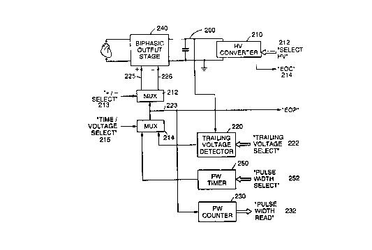
Referring to Fig. 2, in the illustrated
embodiment of the invention, a control system is used
which comprises functional modules and addresses that
the microprocessor can read or write.
Fig. 3 is a flow diagram that will be used in
conjunction with the Fig. 2 block diagram to describe
how a biphasic waveform having selected constant tilt
positive and negative pulses can be generated.
~eferring to Figs. 2 and 3 at step 300 of the
Fig. 3 flowchart, the microprocessor decides that a
defibrillation output is necessary. This could be
due to the automatic detection of fibrillation by the
device, or due to an external command from the
physician, or due to any other reason.
Before a pulse can be delivered, energy must be
stored on the defibrillation capacitor 200 (Fig. 2),
which typically has a value of about 150 microfarads.
At step 310, the microprocessor addresses the
high voltage converter 210 to command it to start
charging the defibrillation capacitor 200 to a
selected voltage (address "select HV" 212).
At step 312, the microprocessor starts a polling
loop by reading "EOC" 214. "EOC" is the "end-of-
convert" signal from the high voltage converter 210
and s$gnifies that the converter has finished
charging the capacitor 200 to the selected initial
voltage. After reading "EOC" at step 312, the
microprocessor determines if the initial high voltage
iB ready at step 314.
If the initial high voltage is not ready, then
the m$croprocessor loops ~ack to step 312. In some
implementations it may be desirab-le for the
microprocessor to attend to other tasks or to be
disabled for periods to conserve current during
polling loops. If, at step 314, the microprocessor
~ 3 ~ 5j~
PATENT
-7-
finds that the defibrillator capacitor 200 is charged
to the selected initial voltage, then the
defibrillation system is prepared for delivery of a
positive pulse.
The pulse width of the positive pulse is
deteL ine~ by the length of time required for ~he
defibrillator capacitor to decay to a selected decay
voltage. If, in this illustrative example, the
selected peak voltage is 500 volts, then 200 volts
would be a reasonable decay voltage for the trailing
edge voltage of the positive pulse to assure an
effective negative phase (a trailing edge voltage of
100 volts for the negative phase will be used for
thi~ example).
At step 316, the microprocessor man~pulates the
controls of two multiplexers 212 and 214 to set the
output stage to terminate the positive pulse when the
selected trailing edge is detected on the
defibrillation capacitor 200. Multiplexer 212
selects the signal flow to either generate a positive
pulse or a negative pulse.
At step 316, the microprocessor addresses "+/-
select" 213 to choose a positive pulse. Multiplexer
214 selects the signal flow to either produce a pulse
with a selected time duration or a pulse which
terminates when a selected decay voltage is detected
on the defibrillator capacitor 200 At step 316, the
microprocessor addresses "time/voltage select" 215 to
choose a pulse which terminates when a selected decay
voltage is detected.
The positive pulse is started by the
microprocessor at step 318 by addressing "Trailing
voltage select" 222 and setting the selected trailing
edge voltage to 200 volts. Since the voltage on the
defibrillator capacitor 200 is at 500 volts, the
J ,'~
PATENT
-8-
output 221 of the trailing volta~e detector 220 goes
high. This signal 221 goes through multiplexer 214
to line 223, through multiplexer 212 to the positive
pulse input 225 of the biphasic output stage 240
which generates a positive defibrillation output as
long as positive pulse input 225 is asserted.
Once the positive pulse is started, the voltage
on the defibrillator capacitor starts to decline as
current flows into the patient's heart 290. Trailing
voltage detector 220 maintains signal 221 high until
the voltage on the defibrillator capacitor 200 has
decayed to less than the trailing voltage selected by
address 222. In this example, when the capacitor
voltage decays to 200 volts, the trailing voltage
detector 220 responds by forcing its output 221 low.
This signal goes through multiplexer 214, line 223,
and Trailing voltage detect 222 to the positive pulse
input control 225 of the biphasic output stage 240,
terminating the positive pulse.
While the positive pulse is being generated, the
microprocessor waits in a polling loop for the pulse
to end. The microprocessor reads "EOP" at step 320.
"EOP" is the "end-of-pulse" signal and is the same as
line 223 dlscussed above. As long as the pulse is
being generated, "EOP" is high; when the pulse is
over, "EOP" goes low. Having read "EOP" at step 320,
the microproces~or checks to see if the pulse is over
at step 322. If the pulse i5 not over, the
~icroprocessor loops back to step 320. When the
po~itive pulse ends, the microprocessor sets up the
de~ibrillator system to produce the negative pulse.
At step 324, the microprocessor addresses the
~ select" 213 multiplexer 212 to select a negative
pulse. The negative pulse is started by the
microprocessor at step 326 by addressing "Trailing
PATENT
_g_
voltage select" 222 and setting the selected trailing
edge voltage to 100 volts (in this ~xample). Since
the voltage on the defibrillator capaci~or 200 is at
200 volts, the output 221 of the trailing voltage
detector 220 goes high. This signal 221 goes through
multiplexer 214 to line 223, through multiplexer 212
to the negative pulse input 226 of the biphasic
ou~yu~ stage 240 which generates a negative
defibrillation output as long as negative pulse input
226 is asserted.
once the negative pulse is started, the voltage
on the defibrillator capacitor 200 starts to decay
again as current flows into the patient's heart 290.
Trailing voltage detector 220 maintains signal 221
high until the voltage on the defibrillator capacitor
200 has decayed to less than the trailing voltage
selected by address 222. In this example, when the
i' capacitor voltage decays to 100 volts, the trailing
voltage detector 220 responds by forcing its output
221 low. This signal goes through multiplexer 214 to
line 223 and Trailing voltage select 222 to the
negative pulse input control 226 of the biphasic
out~u~ stage 240, terminating the negative p~lse.
While the negative pulse is being generated, the
mi~uprocessor waits in a polling loop for the pulse
to end. The microprocessor reads "EOP" at step 330.
As long as the pulse is being generated, "EOP" is
high; when the pulse i8 over, "EOP" goes low. Having
read "EOP" at step 330, the mi~opYocessor chec~c to
see if the pulse is over at 332. If the pulse is not
over, then the microprocessor loOp8 back to step 330.
When the negative pulse ends, the micLop~ocessor
exits the pLoy~am flow at step 390.
Fig. 4 is a flow diagram that will be used in
con~unction with the Fig. 2 block diagram to describe
PATENT
--10--
how a biphasic waveform having a positive pulse of
selected constant tilt and a ~ ve pulse duration
related to the positive pulse duration can be
generated. Generation of the positive pulse is
accomplished in the same manner as described above in
conjunction with Fig. 3, but is repeated here for
completeness.
At step 400, the microprocessor decides that a
defibrillation output is necessary. Before a pulse
can be delivered, however, energy must be stored on
the defibrillation capacitor 200, which typically has
a value of about 150 microfarads. At step 410, the
microprocessor addresses the high voltage converter
210 to command it to start charging the
defibrillation capacitor 200 to the selected initial
voltage (address "select HV" 212).
At step 412, the microprocessor starts a polling
loop by reading "EOC" 214. "EOC" is the end-of-
convert signal from the high voltage converter 210
and signifies that the converter has finished
charging the capacitor 200 to the selected voltage.
After reading "EOC" at step 412, the microprocessor
determines if the high voltage is ready at 414.
If the high voltage is not ready, then the
microprocessor loops back to step 412. In some
implementations, it may be desirable for the
microprocessor to attend to other tasks or to be
disabled for periods to conserve current during
polling loops. If, at step 414, the microprocessor
finds that the defibrillator capacitor 200 is charged
to the selected initial voltage, then the
defibrillator system is prepare~ for delivery of a
positive pulse. The pulse width is determined by
the length of time required for the defibrillator
capacitor to decay to a selected decay voltageO If,
~ ~~J~ ~
PATENT
--11--
in thi~ illustrative example, the selected peak
voltage is 500 volts, then 200 volts would be a
reasonable target voltage for the trailing edge
voltage of the positive pulse to assure an effective
negative phase.
At step 416, the microprocessor manipulates the
controls of two multiplexers to set the output stage
to terminate the pulse when the selected trailing
edge is detected on the defibrillation capacitor 200.
Multiplexer 212 selects the signal flow to
either generate a positive pulse or a negative pulse.
At step 416, the microprocessor addresses "~/-
select" 213 to choose a positive pulse. Multiplexer
214 selects the signal flow to either produce a pulse
with a timed duration or a pulse which terminates
when a selected decay voltage is detected on the
defibrillator capacitor 200. At step 416, the
microprocessor addresses "time/voltage select" 215 to
choose a pulse which terminates when a selected decay
voltage is detected.
, The positive pulse is started by the
microprocessor at step 418 by addressing "Trailing
volta~e select" 222 and setting the selected trailing
edge voltage to 200 volts ~in this example). Since
the voltage on the defibrillator capacitor 200 is at
500 volts, the output 221 of the trailing voltage
detector 220 goes high. This signal 221 goes through
multiplexer 214 to line 223 and through multiplexer
212 to the positive pul~e input 225 of the biphasic
o~u~ stage 240 which generates a positive
defibrillation Gu~pUt as long as positive pulse input
225 is asserted.
- once the positive pulse is started, the voltage
on the defibrillator capacitor starts to decline as
current flows into the patient's heart 290. Trailing
~ 9~ r 2 ~
PATENT
-12-
voltage detector 220 maintains signal 221 high until
the voltage on the defibrillator capacitor 200 has
decayed to less than the trailing voltage selected by
address 222. In this example, when the capacitor
voltage decays to 200 volts, the trailing voltage
detector 220 responds by forcing its output 221 low.
This signal goes through 214, 223, and 222 to the
positive pulse input control 225 of the biphasic
ou~p~ stage 240, terminating the positive pulse.
While the positive pulse is being generated, the
microprocessor waits in a polling loop for the pulse
to end. The microprocessor reads ~'EOP" at step 420.
"EOP" is the end-of-pulse signal and is the same as
line 223 discussed above. As long as the pulse is
being generated, "EOP" is high; when the-pulse is
over "EOP" goes low. Having read "EOP" at step 420,
the microprocessor checks to see if the pulse is over
at step 422. If the pulse is not over, then the
microprocessor loops back to step 420. When the
positive pulse ends, the microprocessor sets up the
hardware to produce the negative pulse which is to
have a duration related to the positive pulse (in
this example, the negative pulse will be set equal in
duration to the positive pulse).
Since the positive phase pulse was terminated by
the capacitor 200 reaching a selected decay voltage
~200 volts in this example), the pulse duration is
dependant upon the impedance of the patient's heart.
For example, a comparatively low impedance of 25 ohms
would result in a shorter pulse duration o~ about 3.4
milliseconds (for a 150 microfarad capacitor 200),
while a 50 ohm patient ; ed~nce would result in a
pulse duration of 6.8 milliseconds.
once the positive pulse is over, at step 430 the
microprocessor addresses the pulse width counter 230
~3~ '',rl ~J
PATENT
-13-
(address "pulse width read" 232) to determine the
positive phase pulse duration. The pulse width
counter 230 measures the duration of "EOP" 223.
Thus, the address "pulse width read" 232 contains the
duration of the positive pulse. The microprocessor
stores the duration of the positive pulse width for
future use.
At step 432, the microprocessor manipulates the
controls of two multiplexers 212 and 214 to set the
output stage to produce a negative pulse with a timed
duration. Multiplexer 212 selects the signal flow to
either generate a positive pulse or a negative pulse.
At step 432, the microprocessor addresses "+/-
select" 213 to choose a negative pulse. Multiplexer
214 selects the signal flow to either produce a pulse
with a timed duration or a pulse which terminates
when a selected decay voltage is detected on the
defibrillator capacitor 200. At step 432 the
microprocessor addresses "time/voltage select" 215 to
choose a pulse with a timed duration.
The negative pulse is started by the
microprocessor at step 434 by writing to the pulse
width timer 250 address "pulse width select" 252)
The pulse width timer produces a pulse of a duration
which the microprocessor sets by writing a value to
address "pulse width select" 252. In this example,
the microprocessor makes the duration of the negative
phase the same as the duration of the positive phase.
To do this, the microprocessor writes into the pulse
width ti~er 250 the value of the positive phase
duration which it read from "pulse~width read" 232
and stored. If the microprocessor was to make the
negative phase twice the duration of the positive
phase, then the microprocessor would multiply by two
the positive phase duration (which it read from
PATENT
-14-
"pulse width read" 232 and stored) before writing it
into the pulse width timer 250. As ~hould be clear,
the negative phase duration can be made related in
any mathematical way to the positive phase duration
by manipulating the data representation of the
positive phase duration read from "pulse width read"
232.
By writing ~o the pulse width timer 252, at step
434, the microprocessor starts the negative pulse.
The pulse width timer 250 produces a pulse the
duration of which is set by the data the
microprocessor wrote to address "pulse width select"
252 (which is equal to the positive pulse duration
read from address "pulse width read" 232 in this
example). The pulse from the pulse width timer 250
passes through multiplexer 214 and multiplexer 212 to
the negative pulse input 226 of the biphasic output
stage 240. The biphasic output stage 240 applies the
negative phase output to the heart 290 for as long as
its input 226 is asserted.
While the negative pulse is being generated, the
microprocessor waits in a polling loop for the pulse
to end. The microprocessor reads "EOP" at step 440.
As long as the pulse is being generated, "EOP" is
high; when the pulse is over, "EOP" goes low. Having
read "EOP" at step 440, the microprocessor checkA to
see if the pulse is over at step 442. If the pulse
is not over, then the microprocessor loops back to
step 440. When the negative pulse ends, the
ml~,o~rocessor exits the pLo~-~a~ flow at step 490.
As should be apparent, many combinations of
selected constant tilt and selected constant duration
(or related duration) multiphasic waveforms can be
produced under microprocessor control using the
apparatus disclosed above.
PATENT
-15-
Thus, it should be understood that various
alternatives to the ~ ho~; ?nts o~ the invention
described herein ~ay be e~ployed in practicin~ the
invention. It is intended that the following claims
define the scope of the invention and that methods
and apparatus within the scope of these claims and
their equivalents to covered thereby.
" ' '
:,'- ' ' ~ '