Note: Descriptions are shown in the official language in which they were submitted.
~0 ~/14~ PCT/NO90/~
2057903
PULSATING INFRARED RADIATION 80URCE
This invention relates to pulsating infrared radiation
sources, particularly concerning their applications in infrared
spectral analysis and in thermal printers. By designing the
radiation source as given in this specification, one obtains
larger temperature contrasts and smaller time constants than from
similar sources presently known. This simplifies the making and
improves the performance of equipment encompassing such sources.
All bodies and objects having a certain temperature emit
thermal, electromagnetic radiation. For ideal black bodies, the
emitted power per unit area within a wavelength interval ~A at
wavelength A is given by Planck's radiation law,
hc
(1) W(A,T)~A = 2~ha ( e k~A ~
in which T is the body's temperature, h is Planck's constant, k
is Boltzmann's constant and c the velocity of light: W(A,T) is
termed the spectral radiant excitance of the body. The spectral
distribution of such thermal radiation has a pronounced maximum
at a wavelength A , which to good approximation is determined
by the body's temperat~re through Wien's displacement law,
(2) T-~ = 2897.9 [K.~m].
mox
Thus with increasing temperature, the maximum point of the
distribution becomes displaced towards shorter wavelengths
according to (2). At either side of the maximum, the spectral
distribution falls off strongly, very rapidly for decreasing A
and more slowly for increasing A's.
Integration of (1) across all wavelengths A gives
Stefan-Boltzmann's law for the total radiant excitance of the
body,
(3) W=~T4 ~
WO ~/14~ PCT/No90/OO~K
2~5790~ - 2
~,
where ~ = 5,67-10 12 [W/cm2K4] is the Stefan-Boltzmann constant.
For a lOOo K radiator this corLe~G"~s to approximately
5 ~W/cm2]. Bodies not ideally black are most conveniently
described by introducing a function ~ < 1 on the right hand side
of eqs. (1) and (3); ~ is termed the emissivity of the body.
Materials whose E iS independent of A are called grey emitters.
When a body at temperature T is subjected to temperature
variations of magnitude ~T, corresponding variations are produced
in the body's radiant excitance. At constant wavelength ~, W(~,T)
always increases with rising temperature. Such spectral radiant
contrast is largest in a range near ~ . At the same time, the
total radiant excitance W of a grey body varies by an amount
(4) ~W = 4~oT3~T.
In infrared spectroscopy as well as in thermal printers,
large and rapid variations in radiative intensity from the
thermal source are desireable. The classical infrared radia~ion
sources, however, like Nernst and Globar radiators,~operate at
constant temperatures. That is also the case with more modern
radiation sources, in which thin and electrically conducting
films have been deposited onto thermally insulating substrates,
cf. British patent 1.174.515, US patents 3.694.624 and 3.875.413,
and German Auslegeschrift 24.42.892. Variations in radiative
intensity are then afforded by means of mech~ically moveable
shutters (choppers) interrupting the radiation. This results in
large contrast in radiation between the hot source and the cold
chopper blade. But it also constrains temperature variations to a
fixed frequency, introduces complicating mech~n;cally moveable
parts, and obstructs electronic control of the radiation source
contrary to other circuit components.
Norwegian patent 149.679 describes a pulsating infrared
radiation source, comprising an electrically insulating substrate
onto which has been deposited an electrically conducting film,
~O90/145~ PCT/NO~/~
- 3 _ 20~ 790 3~
where the thermal time constant of the source - given by the time
required for thermal diffusion through the substrate - has been
adjusted to suit the pulse frequencies at which the source is to
operate. The source should then be made so thick as to thermally
insulate, for the duration of the current pulse, the rear side of
the substrate from the electrically conducting film on the front
side. At the same time the source must be sufficiently thin to
support heat diffusion through the substrate between pulses. This
gives sources with typical substrate thicknesses of 0.1 - 1 mm.
However, radiation sources whose thicknp~ces are as given in
the mentioned Norwegian patent, have thermal responses mainly
determined by the substrate's thermal capacity. This may be
illustrated by a 0.5 mm thick and 1 cm2 wide substrate, made from
a material with specific gravity 2 [g/cm3] and specific thermal
capacity 0.5 ~J/g-X], which stores 0.5 J of thermal energy per
lo R temperature difference. If the source is used to produce
thermal radiation at 50 Hz, 25 W of electrical energy needs to be
supplied. But at a temperature of 1000 K, from (3) only 5 W of
thermal power may be radiated, and only 0.2 W concurrent with the
temperature variations according to (4). Energywise such a source
thus is very inefficient. The majority of the electrically
supplied energy becomes stored as heat in the substrate, to be
continuously conducted away through the rear side and the ends,
nearly 20 % is lost as CW radiation, and less than 1 ~ of the
energy leaves the source as the desired radiation at 50 ~z. The
source is also prone to mP~ ;cal fracture, since the periodic
temperature differences between its front and rear sides subject
the substrate to repeated bending strains.
US patent no. 3.961.155 describes an element for thermal
printers, whose main components are chiefly those of the source
described above. The substrate's thickness is typically 0.5 mm,
the element thus being subject to the same limitations as apply
to sources according to Norwegian patent no. 149.679. None of the
mentioned patent specifications solve the central problem about
-- 20~19~3
pulsating thermal radlatlon sources, whlch ls to achleve large
temperature contrasts at arbltrarlly chosen pulse frequencles.
The present lnventlon takes as its startlng polnt
that a large temperature contrast ls, chlefly, a questlon of
coollng the source between current pulses. Thls can be
achleved by maklng the source radlatlon cooled, contrary to
the sources dlscussed above whlch are cooled by heat
conductlon. Conductlon of heat occurs by dlffuslon, whlch ls
a slow process, whereas thermal radlatlon ls essentlally
lnstantaneous. The source must then be deslgned to make most
of the electrlcally supplled energy radlate away thermally
- durlng the flow of the current pulse. A prlorl thls results
ln a hlgh thermal efflclency of the source, slnce the useful
radlatlon ls the same as that whlch cools the source.
Ideally, then, very llttle thermal energy remalns stored ln
the source after the current pulse, whlch energy ls even
further removed through contlnued thermal radlatlon. Thls
happens ln a tlme lnterval that may be short compared to the
duratlon of the current pulse, resultlng ln a rapld and large
drop ln temperature after each current pulse.
In summary, the present lnventlon provldes an
lnfrared radlatlon source comprlslng a thln, plate shaped and
at least partly electrlcally conductlve element, and
energlzlng means for energlzlng the electrlcally conductlve
part of the element wlth pulsatlng electrlc current, whereby
to vary the temperature of the element between a hlghest and a
lowest value, characterlzed ln that the physlcal thlckness of
the element ls so small that thermal energy stored ln the
~- ~ 28415-1
- 2057903
element durlng one pulse of the electrlc current ls less than
thermal energy radlated from the element ln the course of the
same pulse of the electrlc current.
Thus, ln a radlatlon cooled source accordlng to the
lnventlon, the thermally stored energy ls less than and
preferentlally slgnlflcantly less than the thermal energy
radlated durlng each current pulse. Such sources are so thln
that they become unlformly heated throughout thelr volume,
thus they are also radlatlon cooled to both sldes.
In a preferred embodlment the thlckness t of the
source must satlsfy the relatlon
(5) t < 8~T3/C~ ,
whlch ls derlved from equatlon (4) and where C ls the speclflc
thermal capaclty of the source materlal, ~ lts denslty and f
the pulse frequency of the deslred radlatlon. For a materlal
as ln the example above, wlth C = 0.5 [J/g-K], ~ = 2 [g/cm3]
and~ = 1, one flnds t c 4 1~m for f = 100 Hz. Thls ls two
orders of magnltude thlnner than for sources as earller
- 4a -
28415-1
WO ~/145~ PCT/N090/~
~ _ 5 _ 205 7 ga ~- ~
described, which serves furthermore to emphasize the novelty of
the basic conditions here laid down for the construction of
efficient sources for pulsating infrared radiation.
A more detailed presentation of the invention is given
below. Reference is made to the drawings, in which all relative
measures may be distorted and where
Figure l schematically shows the design of a radiation source
with leads for electrical current,
Figure 2 shows a source consisting of an electrically conducting
film deposited onto a nonconductive material,
Figure 3 depicts an idealized cut through a source, emphasizing
optical relations of importance for its functioning,
Figure 4 depicts a source contained in a housing with a window
for the transmission of thermal radiation,
Figure 5 shows the use of a source contained between two
windows, with associated drive circuit for the source
and detection system for the radiation.
Figure l depicts a source lO with physical thickness ll as
shown, with electrical supply leads 12 and 13 coupled onto
electrical contacts 14 and 15 on the source. To make the source
work as intended, its physical thickness must satisfy the
conditions formulated in claims l or 2. In principle, all sources
according to claims 4 - 7 are shaped as in Figure l, being
basically plate formed with physical thicknesses very much
smaller than their length and width dimensions.
Often the source may be so thin as to be partially
transparent to its own radiation. This lowers the effective
emissivity. To counteract that, it may be advantageous to make
the sources described in claims 4 - 8 as thick as possible,
subject to claims l or 2. In practical circumstances, suitable
optimum combinations may have to be sought in each separate case.
WO ~/145~ PCT/NC~O/~
~ S~ g~3- ~ ~ 6 -
An interesting eventuality with such thin sources is to have
them made from various resistance metals and alloys, for instance
combinations of Ni, Cr and Fe, thus retaining sufficient ohmic
resistance to heat the sources electrically to elevated
temperatures. This possibility is expressed in claim 4. At the
same time, such metals and alloys may have high emissivities,
above 0.8 for Ni-Cr-Fe and more than o.9 when oxidized, as
specified in claim 5, particularly at high temperatures.
Claim 4 also specifies another relevant source material,
metallic glasses, possibly oxidised according to claim 5. These
are alloys into which have normally been mixed transition metals
and nonmetals, shock cooled from fluid state to preserve the
amorphous structure. Metallic glasses are preferentially made
into thin foils, with electrical resistances that may vary widely
through choice of alloying components. In addition, metallic
glasses have good anticorrosion properties. Problems may occur
due to recrystallization of the metallic glass when temperatures
reach above certain limits. Presently such materials would,
therefore, mostly be suitable for sources that operate at
relatively low temperatures.
A third relevant alternative is to use semiconductor
materials to produce sources according to Figure l, as specified
in claim 6. These may be made into the desired thicknesses
through st~n~Ard etching te~hn;ques. Under normal conditions,
several semiconductors may be transparent to infrared radiation,
and so are extensively used as optical materials in the infrared.
At sufficiently strong doping, however, the semiconductor may
acquire so many free charge carriers that it approaches a metal,
electrically speaking. Its electric resistance thus may be
controlled through doping. Simultaneously the material's
absorption of infrared radiation becomes strongly enhanced,
resulting in similar increase of its thermal infrared emissivity.
The strongest possible doping may often be advantageous, since
that multiplies the number of charge carriers, lowers the
WO ~/145~ PCT/NO90/0~ ~
_ 7 _ 20~79~3
transparency and increases the source's emissivity to an optimum.
Limits for the practically useful doping will be set by the
electrical requirements on the drive circuit 56 for the source,
cf. Figure 5 below.
Another alternative embodyment of a source according to
Figure l may be to make it from a basically non-conductive
material, with one or more electrically conductive materials
added as specified in claim 7. Ceramics would constitute
particularly relevant starting materials for such sources, in
that many ceramics have high melting points and advantageous
thermal properties in general, with material structures that
allow their composition to be varied within wide limits.
Figure 2 depicts a~source that consists of, chiefly, an
electrically non-conductive substrate 20, onto which has been
deposited an electrically conductive film 22, with electrical
contacts 23 and 24 and supply leads 25 and 26, and whose total
physical thickness 21 satisfies claim l or 2. In relation to
claim 2, it will be the average or effective density and specific
thermal capacity of the material combination that enter into the
mathematical relation (5) for the thickness of the element. An
alternative may be to choose a substrate material that is opaque
in the actual spectral region for the source, so that the
substrate emits thermal radiation. Possible materials could be,
e.g., quartz, alumina and various ceramics, or a thermally
resistent glass like Zerodur. Whenever desired, the electrically
conductive film may then be made so thin as to not noticeably
influence the thermal - and to a limited extent only the optical
- properties of the source. Alternatively, a substrate material
might be chosen that is transparent to the relevant infrared
radiation. The electrically conductive film would then have to
serve as emitter, too, and could if nec~s~ry be made thicker at
the expense of the substrate thickness in order to increase the
emissivity. Claim 8 describes both alternatives.
~oS1 g ~ - 8 - PCT/No~O/~86
As a result of claims 1 and 2, the sources normally may have
thickne~ces that are comparable to the wavelengths of the
radiation to be generated. In addition, as said above, they may
often be partially transparent to the radiation. As in any other
electromagnetic structure, this leads to strong interference
effects, particularly in directions normal to the element's
surface, which is also the main direction of radiation. Figure 3
thus depicts an idealized cut through a source 30, with physical
thickness 31 and optical thickness 32, the optical thickness
being a product of the physical thickness with the material's
index of refraction. Radiation is also shown as emitted from a
point 33 inside the source, with reflections 34 and 35 from the
surfaces and transmitted rays 36 and 37. Such reflections result
in noticeable interference effects, which may be quite pronounced
in materials with large refractive indices, like semiconductors.
It may therefore be advantageous to use materials with relatively
low indices of refraction, to reduce the surface reflections.
Simple antireflection coatings may be introduced, particularly
for comparably thick sources and short wavelengths, but only at
the expense of the substrate thickness and thus may serve to
reduce the effective emissivity.
The interference problem may often be minimized if the
optical thickness of the source equals a multiple of half the
radiative wavelength, as specified in claim 3. In a solid angle
around the normal to the surface, this gives constructive
interference which maximizes radiation in the selected spectral
interval. Minor thickness variations among sources during
production shall not, then, lead to significant changes in the
directional and emissi~n characteristics of their thermal
radiation at the chosen wavelengths. In order to maintain
reproducible conditions, therefore, the interference problem may
require sources for different spectral regions to be made with
different thicknesses. This also is a new feature in relation to
the mentioned existing radiation sources.
WO90/145~ PCT/NO90/~
9 20579~0~
Figure 4 depicts a source 40, with electrical supply leads
41 and 42, mounted within a hermetically sealed container 43
devoid of reactive gases, so that the source may not change its
character during operation. As specified in claim 9, it may often
be an advantage to mount two or more sources inside the same
housing, to change quickly between two or more wavelengths. The
housing, which is made from a thermally well-conducting material,
encompasses active or passive external cooling means 44 and 45,
and has a window 46 that is transparent to infrared radiation. It
is a main point about this invention to cool the source between
current pulses, thereby to achieve large ~un~asts in radiation.
As long as the source is freely suspended and may radiate without
physical obstructions, this presents no problem. The radiation
then serves to cool the source, as explained above. With the
source mounted inside a container, which may be quite practical,
the latter may restrict the radiation leaving the source, and
thereby restricts also its cooling. This is a new problem
relative to existing sources operated at constant temperatures,
in which the housing conducts away most of the supplied energy,
and where the temperature of the container may approach that of
the source without causing problems for the source's operation.
The source can at no time be colder than its surroundings,
which are heated by the source. To make the source reach a low
temperature between current pulses, the housing as well as the
window must be kept colder than the lowest temperature to be
reached by the source when in use, as specified in claim 9. The
source shall then have a net heat loss between pulses, too. As
far as the housing is concerned, this may be achieved by making
its internal walls mirror-like, in addition cooling the housing
externally. Radiation from the source shall then mainly be
reflected back onto the source or out through the window, while
that which becomes absorbed in the walls is conducted away.
As is in addition specified in claim 9, it is also a
condition for efficient cooling of the source that the window is
WO ~/14~ PCT/No90/~86
Sr~ 3
transparent across a spectral range that includes the major parts
- and preferentially more than 90 % - of the total thermal
radiation from the source. This, too, is a novel feature compared
to existing sources that operate at constant temperatures. For
those it is only required that the window be transparent for that
particular spectral range which the source delivers. Radiation
from the source outside of that spectral region then becomes
absorbed in the window to heat it, so that the window may radiate
back onto the source to keep it hot. This would make it difficult
to cool the present source between current pulses. For the
radiation source to work properly, all thermal radiation should
be able to leave the source without hindrance. For instance, to
transmit so % of the thermal radiation, the windows must be
transparent across a whole decade centered at ~m~x , as given by
the source's peak temperature according to (2). For a source to
work at 3 ~m wavelength, useful windows thus should preferably be
transparent in the region 1 to 10 ~m. Sources working at elevated
temperatures of 1000 K and above, require the windows to be
transparent down to, and possibly into, the visible spectral
region. Low index window materials may be advantageous, to avoid
retroreflections from window surfaces that might reduce the
radiative cooling. Broad band anti-reflection coatings centered
around ~ may also be useful in that context.
max
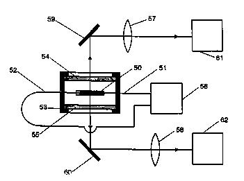
Figure 5 shows one or more sources 50, with electrical
supply leads 51 and 52, mounted in a housing 53 with two windows
54 and 55 as specified in claim 10. In other respects the housing
and the windows have the same properties as specified in claim 9.
Since the source is so thin as to radiate equally well to both
sides, this embodyment may be the one that best satisfies the
requirements on efficient radiative cooling. The design also
makes it possible to utilize the radiation from both sides of the
source, as shown in the figure. Schematically shown, too, is an
electric drive circuit 56 for the source, as well as lenses 57
and 58 and mirrors 59 and 60 to guide the~radiation onto
detection equipment 61 and 62. Such equipment is relevant when
WO90/145~ PCT/NO~/O~
- - 11 - 20~7903
the source is being applied to infrared spectral analysis, e.g.,
for the detection of gases. The two sides of the source may then
be employed to produce radiation at two different wavelengths, or
the radiation from one side may be used as a reference against
which to identify minor changes in radiation from the other side
when traversing a volume of gas. In both cases, as in several
different examples that may easily be imagined, a source with two
windows offers obvious constructive benefits, while economizing
on radiation since beam splitters may not be required.
The present invention thus enables one to produce pulses of
infrared radiation, with practically constant intensity, up to
the frequency f that enters into relation (5). The source may
thereby be electronically controlled like any other circuit
element. It may then also be possible, e.g., to pulse code the
radiation from such an element. This will make the source useful
in termal printers, while such coding may also be exploited in
more advanced spectroscopic connections. Moreover, for a given
radiative intensity, the source requires significantly less
energy supplied than do similar known sources. Further and
substantial constructive simplifications, in spectroscopic and
analytic equipment, may be realized by utilizing the radiation
from both sides of the source.
-- O --