Note: Descriptions are shown in the official language in which they were submitted.
20~81~3
w
DIRECT MICROCIRCUIT DECOUPLING
BACKGROUND OF THE INVENTION
The invention disclosed herein relates
generally to decoupling capacitors for use with
integrated circuits.
In the past decoupling capacitors for
integrated circuits have sometimes been separate
devices mounted on a printed wiring board and wired
across the power supply and return connection to the
dual in-line or other type integrated circuit
package.
Inductance is dependent on the loop area
through which current flows and the magnetic flux
through the loop. Voltage drop due to inductance is
equal to Ldi.
dt
~ In the past approach of a separate
capacitor on the circuit board the length of the
path that the current must flow through from the
capacitor to reach the chip contributes to the
voltage drop due to Ldi.
dt
Another past approach has been to mount a
decoupling capacitor on the chip package to reduce
the lead length between the capacitor and the chip.
While past methods provide adequate decoupling for
-1-
:20~5~1~3
~.
many applications, there are other applications that
require improved decoupling.
An example of such an application is the
need for certain integrated circuit devices to be
insensitive to being bombarded by ionizing
radiation. A basic effect of the ionizing radiation
is to generate electron-hole pairs in the
semiconductor material. In an integrated circuit
having a power supply voltage reference and a ground
reference, the effect of being irradiated is to
create a high current flow in the chip between the
voltage reference and the ground reference. The
further effect is for current flowing from the power
supply to encounter inductance in the connecting
leads from the power supply. The result is that the
on-chip voltage essentially collapses.
A solution is to place a capacitor across
the integrated circuit as close as possible to the
integrated circuit so that the capacitor is charged
to the chip power supply voltage. Then when a
transient due to radiation or any cause occurs, the
board capacitor is available to supply current
instantaneously to the integrated circuit. Thus a
need exists for a decoupling device that can be
placed as close as possible to the integrated
circuit.
-a~
SUMMARY OF THE INVENTION
The present invention solves these and other needs
by providing a decoupling apparatus that is placed directly
onto a passivated surface of an integrated circult chip.
The present invention allows a custom capacitor to
be located directly on the upper surface of the chip or
alternatively for the capacitor to be located below the chip.
An alternative arrangement provides for the use of
standard chip capacitors on the surface of the chip. Metal
bars placed on the passivated chip surface make the chip power
supply and power return or ground accessible. Wire bond
connections extend from the metal bars to the capacitor
terminals.
In accordance with the present invention, there is
provided a microchip having a planar first surface, a power
supply connection means and a power return connection means,
includlng planar decoupling capacitor means having a first
termination means and a second termination means, said planar
capacitor means being secured dlrectly to said first surface
with no intermediate insulating layer; and characterised by
the power supply connection means and power return connectlon
means being connected to a respective elongate metal bar on
sald planar first surface to which a plurallty of wlre bonds
from first termination means and second termlnation means
respectively are connected.
75998-1
:
.~
.~
i7 ~ 3 "
3a
BRIEF DESCRIPTION OF THE DRAWINGS
Figure 1 is a plan view of a decoupling device in
accordance with applicants's invention.
Figure 2 is a side elevation view of the decoupllng
device of Figure 1 according to section line 2-2.
Figure 3 is a plan view of an alternative design of
the decoupling device.
Figure 4 is a side elevation view of the decoupling
device of Figure 3 according to section line 4-4.
_D 75998 1
~'-
.~ .,,~
2058143
Figure 5 is a plan view of a second
alternative design of a decoupling device in
accordance with applicant's invention.
Figure 6 is a side elevation view of the
decoupling device of Figure 5 according to section
line 6-6.
Figure 7 is a variation of Figure 1
showing an alternate capacitor design.
DESCRIPTION OF THE PREFERRED EMBODIMENT
In Figures 1-6, reference numeral 10
identifies a decoupling apparatus in accordance with
applicant's invention.
As shown in Figure 1 microchip 12 has an
upper surface 11 and lower surface 13. Power supply
connection 14 and a power return connection 16 in
the form of bonding pads are located on microchip
surface 11. A combination of a power supply Vdd,
and an adjacent power return Vss, forms a Vdd-Vss
pair. Vdd-Vss pairs are designated 30 and are shown
in Figure 1 located near or along side edges 15 and
17 of surface 11. Microchip 12 also includes
bonding pads 18 for signal connections.
As shown in Figures 1 and 2, custom
capacitor 20 is located directly on passivated
surface 11. Custom capacitor 20 may be physically
attached to surface 11 by any of a variety of
bonding agents. Instead of having only a terminal
- 4-
20~8~L~3
, ~,
at each end, custom capacitor 20 is designed with
pairs of terminals 23 which are made up of
individual terminals 22 and 24 which are of the
bonding pad type. Wire bond 26 connects power
5 supply connection 14 to capacitor terminal 22 and
wire bond 28 connects power return connection 28 to
capacitor terminal 24. Capacitor terminals 22 and
24 form a pair of terminals 23.
As shown in the drawings, custom capacitor
10 20 is designed with terminal pairs 23 opposite Vdd-
Vss pairs 30.
As shown in Figure 7, as an alternate to
the discrete pairs of terminals 22 and 24,
continuous concentric power and ground rings on the
15 upper surface of the custom capacitor 31 would allow
a more universal capacitor design where the wire
bond pairs 23 could be placed as required by the
microchip 12.
In a first alternate design approach as
20 shown in Figures 3 and 4, microchip 12 ' has an upper
surface 11'; lower surface 13'; power supply
connection 14 ' and power return connection 16'.
Power supply connection 14 ' and power return
connection 16' are in the form of bonding pads
25 located on microchip upper surface 11'. A
combination of a power supply 14 ' or Vdd and a power
return 16' or Vss form a Vdd-Vss pair which is
- 5 ~
2QS8~4~
..
designated 30'. Vdd-Vsspairs are located near or
along side edges 15' and 17' of surface 11'.
Microchip 12' also includes bonding pads 18' for
signal connections.
As shown in Figures 3 and 4 custom
capacitor 20' is located below microchip 12' and is
secured by a bonding agent directly against surface
13'. Custom capacitor 20' is designed with pairs of
terminals 23' which are made up of individual
terminals 22' and 24' which are of the bonding pad
type.
A second alternative design approach which
utilizes standard chip capacitors is shown in
Figures 5 and 6 for decoupling apparatus 10.
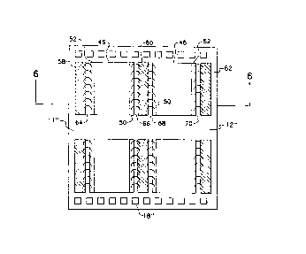
In Figures 5 and 6 microchip 12" has its
upper level metallization designed to bring the
power supply connection and power return connections
to surface 11" at locations which accommodate
standard capacitor sizes. For example, in Figure 6
power supply connections may be brought to 40 and
power return connections brought to 42 and 44.
The second alternative design allows
standard chip capacitors 46 and 48 to be used. For
example, capacitor 46 is a standard chip capacitor
which rests directly on surface 11" of microchip
12". Capacitor 46 has terminals 50 and 52 which
preferably are gold plated.
2~81~3
Metal bars of which 58, 60 and 62 are
typical are gold plated and are located directly on
surface 11" and electrically connected to power
supply 40 and power return 42 by solder bump
connections at 42, 40 and 44. Electrical
connections from metal bars 58 and 60 to capacitor
46 are made by wire bonds 64 and 66 respectively.
Electrical connections from metal bars 60 and 62 to
capacitor 48 are made by wire bonds 68 and 70
respectively.
Metal bars of which 60 is typical provide
a large area contact with passivated surface 11".
This area of contact provides for pressure
distribution during the wire bonding operation.
Therefore the cap attach wire bonds can be made over
active circuitry without damage to the microcircuit
and without chip area impact.
Now that the basic construction of the
present invention has been set forth, certain
features can be set forth and appreciated. The
present invention provides for placing a capacitor
on the chip or die rather than placing the die on
the capacitor. An advantage of this feature is that
the decoupling capacitor can be used as an option
and not added until after package test. With this
approach, capacitors are not wasted on die which
fail the package testing. An additional advantage
2058~3
.,.
of placing the capacitor on the die occurs in
multichip modules. Because the die size determines
the spacing between die there is no need to increase
die spacing to accommodate capacitors which are
larger than the die.
The present invention provides for
electrical connections from the die to the capacitor
at multiple locations or Vdd-Vss pairs as shown at
30 in Figure 1. The adjacent bond wires create
magnetic fields which interact and partially cancel
each other. This results in a significantly lower
inductance and therefore lower Ldl voltage drop.
dt
In addition the present invention allows
the power supply and power return to connect at the
same side of the custom capacitor. This reduces the
inductance of the connection and also results in
lower self-inductance than in conventional
capacitors which have terminations on opposite ends.
Applicant's capacitor on die invention is
especially advantages for multichip module designs.
In one such design a ceramic module is used to mount
multiple die, with routing between the die being
within the ceramic module. Applicant's invention
will allow a custom capacitor to be placed directly
on the individual chip surfaces with no additional
ceramic module surface or printed wiring board
surface required for decoupling capacitor.
20S891~3
In accordance with the foregoing
description, applicant has developed a simple
microcircuit decoupling apparatus that may be easily
incorporated into the design of integrated circuits
when required by the application.
Although a specific embodiment of the
applicant's mechanism is shown and described for
illustrative purposes, a number of variations and
modifications will be apparent to those of ordinary
skill in the relevant arts. It is not intended that
coverage be limited to the disclosed embodiment, but
only by the terms of the following claims.