Note: Descriptions are shown in the official language in which they were submitted.
2058509
Field of the Invention
The present invention relates to solid state threshold switches in general. Moreparticularly, the invention relates to chalcogenide threshold switches having improved
stability and a signifi~ntly reduced first fire voltage, and to methods and m~teri~l~ for their
m~nnf~cture.
Back~eround of the Invention
Threshold switches are devices which change their electrical conductivity in response
to a voltage applied thereacross. Ovonic threshold switches are solid state devices based
upon m~teri~ls and effects first discovered by S.R. Ovshinsky; see for example, "Reversible
Electrical Switching Phenomen~ in Disordered Structures" Physical Review Letters, vol.21,
no.20, November 11, 1968, p.l450(c). Ovonic threshold switching materials have bi-stable
conductivity characteristics. In the absence of an applied threshold voltage, the m?~ten~l~
are in a blocking state and exhibit a high electrical resistivity. Imposition of a voltage
e~ee-ling a specific threshold value causes the materials to switch to a low resistivity
conductivity state, which is many orders of m~gnitllde below the resistivity in the blocking
state, and this state is m~int~in~d provided a minimum holding current flows therethrough;
termin~tion of the holding current cycles the m~teri~l back to the high resistivity state.
Ovonic threshold switching devices exhibit switching speeds of less than 150 pico seconds
and have si,onific~nt use as high-speed transient suppressors as well as in various other
switching applications. The characteristics of these switches and the m~teri~l~ from which
they are f~bric~te~l are disclosed in U.S. Patent Nos. 3,171,591 and 3,343,034, the
disclosures of which are incorporated herein by l~fere,lce.
Threshold switching devices are generally constructed to include a body of switching
m~tçri~l with at least a pair of electrodes operatively disposed on opposite sides thereof.
Control of the characteristics of the switching material is achieved by compositional
mo-lifi~tion and/or mo lifil~tion~ of the local order or other morphological mo~ific~tion of
the switching material. The switching material is designed to have a threshold value and
an electrical resi~t~nl~e suited for a particular application.
"First Fire Voltage" is the voltage which is needed to switch a freshly preparedthreshold switching device from the high resistivity to the low resistivity state. This first
2 20~8S0
fire voltage is typically much higher than the normal threshold voltage manifested by the
switch after first fire. The initial voltage permits morphological relaxation of the material
to occur and thereby restructures the local order of the m~teri~l to a stable configuration.
Once the forming operation has been carried out, the threshold switching voltage remains
reproducible and constant.
In the case where discrete switches are being manufactured, the first fire voltage
phenomenon generally presents at most only a minor problem since, in an initial stage in
the testing of the devices, they are simply exposed to a high voltage pulse and consequently
formed. However, it is often desirable to include threshold switches in array configurations
or in combin~tion~ with other devices and under such circumstances, the first fire voltage
ph~nomenon can present a signific~nt problem. The higher voltage necess~ry to form the
freshly manufactured threshold switches may be sufficiently large so as to darnage other
semiconductor devices connected thereto. Also, if an array of threshold switches is being
first fired, the first switch in the array to achieve its working threshold will then serve to
create a low resistivity current path which prevents the other switches from being properly
formed. To o~ ;o,lle these problems, sophisticated isolation circuitry must be included in
combination with the threshold switches. Another problem presented by the first fire
phenomenon is tied into the fact that the final working threshold voltage of the switch is,
to some degree, a function of the first fire voltage applied to the device and the first flre
voltage required may vary from device to device. Consequently, individual switches in
arrays of threshold switching devices may all manifest somewhat different working
thresholds.
Clearly, problems occasioned by the first fire phenomenon can complicate the useof threshold switching devices in cross-point switching arrays and the like and in
conjunction with other types of devices. Therefore, it would be desirable to provide
threshold switching devices which are free of the effects of this phenomenon. Heretofore,
it has been known to treat chalcogenide threshold switching materials with activated
hydrogen for pul~oses of stabilizing the working threshold of such devices; these techniques
are disclosed in U.S. Patent No. 4,804,490, the disclosure of which is incorporated herein
by reference.
2058~09
In accord with the principles of the present invention, it is now possible to provide
threshold switches which include flu-)rin~te~ ~wiLchillg materials having optimized short
range order and which manifest very little, if any, first fire voltage effects. The present
invention makes possible the widespread utilization of threshold switches in a variety of
circuits and in a variety of electronic devices and makes possible the manufacture of
switching arrays having unifo~ upcllies. These and other features and advantages of the
present invention will be readily apparent from the drawings, discussion and description
which follow.
Blief Desclil)~ion of the Invention
There is ~ close~l herein methods and m~tt-ri~li for manufacturing threshold
switching devices having a lowered first fire threshold. Also disclosed ar improved
switching devices. The ~wi~chhlg device is generally of the type comprising a body of
chalcogenide m~tçri~l disposed bct~ ,en two electrodes.
The method includes the steps of vacuum depositing a chalcogenide material and
exposing the chalcogenide m~teri~l to an atmosphere inclu-1ing fluorine therein. The
chalcogenide material may be exposed to ehe fluorine while it is being vacuum deposited
or it may first be deposited and subsequently exposed to the fluorine c~ nt~ining atmosphere.
The steps of vacuum depositing the chalcogenide material include techniques suchas spun~ring~ glow discharge decomposition and the like. The fluorine containingatmosphere may be generated from free fluorine, or from a fluorine-containing material such
as sulphur hexafluoride, carbon tetrafluoride, germ~nium tetrafluoride or the fluorides of
arsenic, telll-rium or sele ~ While fluorine is a "super-halogen" which is highly reactive
in its ground state the atmosphere may be further activated or energized, for example, by
radio frequency energy, direct current energy, microwave energy or by photochemical or
thermal eX~it~tion of a fluorinç-cont~ining atmosphere. The invention further includes
switching devices of the type which include a body of material comprising tellurium,
gçrm~ninm, sulfur, arsenic, selenium and fluorine. The m;~teri~l~ prepared according to the
process of the present invention will preferably include up to 10 atomic percent fluorine
incorporated therein.
2058509
Brief Description of the Drawin,~s
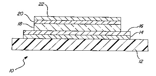
FIGURE 1 is a cross-sectional view of a chalcogenide switching device of the type
which may be advantageously prepared according to the present invention;
FIGURE 2 is a graphic lGp~sentation of the first fire voltage and threshold voltage
of a series of chalcogenide switches pl~pa~ed in accordance with the present invention,
plotted as a function of increasing SF6 concentrations in the deposition atmosphere;
FIGURE 3 is a graphic lcplcsent~tion of first fire and threshold voltages for a series
of switches p~p~,d in accordance with the present invention, plotted as a function of
increasing CF4 concentration in the deposition atmosphere; and
FIGURE 4 is a graphic representation of first fire voltage and threshold voltage for
a series of chalcogenide switches ~ ~cd in accordance with the present invention, plotted
as a function of increasing substrate tempe.atul~,s.
Detailed Des.,~ ion of the Invention
The present invention signifir~ntly lowers the first fire voltage of chalcogenide-based
switching devices to values which applo"illlate the threshold switching voltage of such
devices. As such, the present invention elimin~tes problems which have heretofore made
difficult the use of such devices, particularly in large scale arrays such as cross-point
switching arrays. The present invention may be employed with a variety of chalcogenide-
- based switching matçri~l~ and a variety of switch configurations. It is to be understood that
within the context of the present invention, "chalcogenide m~terial~" or "chalcogenide-based
materials" are meant to include those m~teri~l~ which have one or more group VIa elements
therein. Typically these m~teri~l~ will include elements from groups IV, V and VI and, in
accord with the present invention, may also include some fluorine incorporated therein. A
typical chalcogenide switching material of the present invention will include tellurium,
germanium, sulphur, arsenic, selenium, fluorine and possibly some silicon therein.
There are a variety of switch configurations which have been implemented utilizing
chalcogenide materi~l~, In the most basic form, such switches include a pair of electrodes
in electrical commlmi~ation with a body of chalcogenide material. The device may be
fabricated in a thin film configuration having electrodes disposed on a common substrate
in a coplanar, spaced apart relationship with a body of chalcogenide material overlying
20S85~g
them. In other in~t~nces~ the switching device may comprise a stacked, thin film device
wherein a body of chalcogenide m~teri~l is sandwiched between a pair of electrodes. In yet
other embodiments, the chalcogenide switching device may comprise a bulk device wherein
a relatively large pair of electrodes, such as a pair of carbon buttons, are separated by a
chalcogenide body.
Referring now to Figure 1, there is shown a typical, solid state, high-current-carrying
threshold switching device 10 of the type which may be beneficially fabricated in accord
with the present invention. The switching device 10 of Figure 1 includes a substrate 12
which may be an electrically conductive body such as a sheet of metal or a silicon wafer,
or it may be an electric~lly insulating body such as a sheet of glass or polymer resin and
is preferably of relatively high thermal conductivity.
Deposited atop the substrate 12 is a layer of bottom electrode m~teri~l 14 which, in
one pref~lcd embo liment, comprises a thin film of molybdenum, it being understood that
other conductive m~teri~l~ may be ~imil~rly employed. The molybdenum electrode in this
embodiment is ap~ nately 5,000 Angstroms thick although the precise thickness of the
electrode will be determine~l by the current catTying capacity of the switch. Immediately
atop the layer of bottom electrode material 14 is a body of carbon 16. It has been found,
in accord with the present invention, that inclusion of a carbon layer elimin~tes contact
effects which can interfere with switching of the chalcogenide material. The carbon layer
16 typically has a thi~l~ness in excess of 100 Angstroms and generally falls in the range of
1,000-5,000 Angstroms in thir~nPss In the depicted emboliment, the carbon layer 16 is
4,000 Angstroms thick.
The layer of thin film chalcogenide switching material 18 is disposed atop the carbon
layer 16 of the bottom electrode. The chalcogenide m~teri~l is the active switching element
of the device 10 of Figure 1 and is deposited by a vacuum deposition process in accord with
the principles of the present invention. In the context of this invention, vacuum deposition
processes include sputtering, vacuum evaporation, plasma glow discharge deposition, and
ion or molec.ll~r beam techniques. The thi~kness of the chalcogenide m~teri~l 18 should,
be sl~ffi~ient to provide a continuous cover over the carbon electrode m~teri~l 16. While
there is no minimum thir~ness for the layer, it has been noted that new electronic behaviors
are m~nifested in switching layers of less than 100 Angstroms thickness. The switching
6 2058s~9
threshold of the device will depend upon the composition of the chalcogenide material 18
- as well as its thickness hence, the desired working threshold will govern the ~hi~kness of the
chalcogenide layer 18. In general, the chalcogenide layer 18 has a thicknçss of less than
50,000 An~ ollls. In the illu~llated embodiment, the switching threshold of the
chalcogenide material employed is typically on the order of 30 volts per micron of
conduction path length and the chalcogenide layer 18 is in the range of 5,000-6,000
Angstroms in thickness and the switching threshold is apl)lo~dmately 15-18 volts. As
mentioned hereinabove, the present invention may be employed in conjunction with the
deposition of a wide range of chalcogenide alloys. One particular alloy having si~nific~nt
commercial utility is an alloy compri~e~l of Te36, Ge23, S2l, As~8, Se2. This alloy may also
include up to 10 atomic percent of fluorine and may further include silicon.
The device is completed by a top electrode pair disposed atop the chalcogenide body.
The top electrode pair incllldes a second carbon layer 20 generally similar to the carbon
layer 16 described hereinabove and a top metallic layer 22 generally similar to the bottom
metallic layer 14. In further embodiments, the various layers are subsequently encapsulated
by a protective, electrically insulating m~teri~l such as a layer of an inorganic oxide or
nitride, or a layer of polymeric material. The insulating m~teri~l has access vias
the~llllv~gh communi~ting with the top and bottom electrodes of the device to facilitate
contact thereto.
The principles of the present invention will be illustrated by a series of examples
which follow. The examples detail the fabrication and testing of a number of switching
devices generally similar to that of Figure 1.
Example 1
In this series of examples, the chalcogenide switching bodies of a number of
threshold switches were exposed to increasing concentrations of activated fluorine during
their f~bric~tion and the results are illustrated in Figure 2.
A number of chalcogenide switches generally similar to that of Figure 1 were
plep~,d. The devices were prepared upon glass substrates and in general, the various
layers of the switching device were deposited in sequence while the substrate was
continuously m~int~in~ under a partial vacuum. This helps to ensure that extremely clean
0 5 8 ~ O 9
~_ 7
int~races are forrned between the layers and greatly reduces the chance for any appreciable
amount of c~ n~ tion by air, water vapor, dust or the like. By so doing, the physical
integrity of the interf~ces of assured. Such clean interf~ces are believed to greatly reduce
possible loc~li7ed heating effects and nucleation sites for undesired local crystallization of
the semiconductor materials, which may well adversely affect the electrical stability of the
device.
After chemi(~l cleaning, the substrate is disposed in a vacuum chamber and a lower
molybdenum electrode of approximately 5,000 Angstroms is deposited thereupon by a
conventional ~u~ ;ng process utilizing an argon atmosphere of applu~ llately 4.5 milli-
torr pressure and an applied D.C. power of applu~imately 3 waKs per cm2. After deposition
of the molybdenum layer, a carbon layer of applw~imately 4,000 Angstroms thickness was
slJu~l.,d ther~. ~on under similar con(litions and at total power of 10 watts/cm2.
After the bottom electrode layers are in place, a body of chalcogenide material ofapplox;.~tely 5,100 Angstroms is then deposited atop the carbon. The starting
chalcogenide material in this example comprises Te36, Ge23, S2l, As~8, Se2 and is referred to
herein as a 0027 alloy. The chalcogenide m~t~ l is formed into a sputtering cathode of
apploxi...~tely 3 inches in diameter. The power applied to the cathode is approximately 42
watts at a frequency of 13.45 MHz. The spuu~ g process is carried out in a background
atmosphere of argon m~int~ine~ at a pressure of apl)~u~imately 4.0 milli-torr. In the present
e~e.;.~-ent~l series, increasing concentrations of SF6 were added to the atmosphere used for
the deposition of the chalcogenide.
Following deposition of the chalcogenide material, a top carbon and molybdenum
electrode were deposited. The top carbon electrode was also 4,000 Angstroms thick and the
top molybdenum electrode was 2,100 Angstroms thick. Throughout the depositions, the
substrate was m~int~in.o~l at an elevated lelllpe~atul~e as will be detailed hereinbelow. It is
to be understood that upon deposition of all the layers, the coated substrate may be
advantageously p~ttçrnçd by conventional photolithographic techniques so as to create a
plurality of discrete devices.
Figure 2 summarizes the results of the foregoing e~pe~ lental series. The graph
depicts both first fire voltage, shown by the crosses and threshold voltage after first fire,
shown by the dots. The voltages are all normali7e-1 to volts per micron of current path and
2058509
~_ 8
are plotted against increasing concentrations of SF6 in the chalcogenide deposition
atmosphere. It will be noted that the control samples including no fluorine-containing gas
in the deposition atmosphlre manifested first fire and threshold voltages were approximately
80 and 30 volts per micron, respectively. This is consistent with the behavior of prior art
devices. When the background gas included 2 sccm of SF6, the first fire voltage dropped
to a~proAill-ately 60 volts per micron while the threshold voltage remained at approximately
30 volts per micron. Increasing the amount of SF6 to 3 sccm further decreased the first fire
voltage to approximately 40 volts per micron while the threshold voltage remained at
approximately 30 volts per micron. A further increase of SF6 to approximately 3.5 sccm
resulted in a first fire voltage and threshold voltage which were both appro~in~tely 35 volts
per micron. A further increase in SF6 to 4 sccm produced a device which was initially
shlmte~l i.e., it was in a high conductivity state, but subsequently manifested a threshold of
a~p~ il..ately 28 volts per micron.
It is to be noted that the substrate was m~intainçd at a temperature of approximately
165 C. for the deposition of the material including no SF6 and at 185 C. for the subsequent
depositions. Analysis of the chalcogenide material revealed that approximately 3-4 atomic
percent of fluorine was incorporated into the films. The analysis also in~licated that there
was some slight depletion of gçrmanium and enrichment of tellurium for materials deposited
in the fluorine-cont~ining atmosphere. A specific analysis of the sample prepared with 3.5
sccm of SF6 gave a specific composition of Te33 18 Ge7 38S26 6 AS29 57 Sel 3 and F3 27. In order
to assess whether the improvement in first fire voltage was attributable to a mere shift in
composition, a series of switches were prepared by a sputtering process as in the foregoing
example, but employing a fluorine-free atmosphere and a cathode having the composition
of: Te357 Ge66S274 As2894 and Se~3. A first series of devices deposited on a substrate
m~intainçd at 180 C. inclllde-l a .65 micron thick layer of chalcogenide material and were
all shunted as prepared. A second series was deposited on substrates m~int~ined at room
temp~a~ and included a .70 micron thick layer of chalcogenide material. These switches
had a first fire voltage of 41 volts and a threshold of 16 volts, norm~li7çd to 1 micron
thi~kness The results ~ttend~nt upon the use of fluorine are attributable, at least in large
3~ part to the action of fluorine in optimizing the morphology of the deposited chalcogenide
film. It is further speculated that fluorine acts to configure and/or reconfigure the bonds
~ 9 20585~9
between the components of the chalcogenide film so as to achieve the lowest free energy
of states thereof and to provide a morphology optimized for switching. By so doing, the
implementation of a separate forming stage is elimin~tecl
Exam~le 2
In this experimental series, a number of threshold switching devices were prepared
which were generally similar to those in the previous example; however, carbon
tetrafluoride, CF4, was used as a source of fluorine. Also, the carbon electrode layers were
l,OOO Angstroms thick in this series and the upper molybdenum layer was 2,100 Angstroms
thick. The chalcogenide material was similar to that of the previous experimental series
and ranged in thickness from 5,300-6,400 Angstroms. Substrate temperatures were 185 C.
It will be noted from the graph of Figure 3 that the first fire voltage is approximately
70 volts and the threshold voltage is approximately 15 volts per micron for material
deposited in the absence of any fluorine. When the amount of CF4 is increased toappro~ ately 16 sccm the first fire voltage drops to approximately 40 and the threshold
voltage rises to appl.~i.l-ately 20.
Example 3
In the third series of example, the effective substrate temperature was ascertained.
Again, a series of devices generally similar to that of Figure 1 was prepared in accordance
with the procedure outlined for example 1. The layer thicknesses were approximately equal
- to those of example 1 and depositions were carried out at various substrate temperatures.
It is to be noted herein that the substrate temperatures specified herein are nominal substrate
temperatures. Substrate heating was accomplished by an infrared heater disposed proximate,
but spaced from, the substrate. Temperature is measured by a thermocouple placed close
to the substrate and there may be some deviation between actual substrate temperature
reading and thermocouple readings.
In the experimental series, the SF6 was present in the atmosphere at approximately
2 sccm. It will be noted that the first fire voltage and the threshold voltage come closer
together as a nominal substrate temperature of 160 C. is achieved.
20~8509
~" 10
It is has also been found in accord with the principles of the present invention that
- fluorine-containing gases other than SF6 and CF4 may be simil~rly employed. For example,
elemental fluorine may be advantageously employed in the present invention; however,
fluorine is a somewhat difficult material to handle and accurately meter. Hence fluorine-
cont~ining gases are more generally plefel~d. SF6 is particularly plefe~l~d since the
material being deposited does include some sulfur and hence any residues from the gas will
not present significant cont~min~tion problems. Similarly, CF4 is preferred since any
possible carbon inclusions will not adversely affect the switching characteristics of the
chalcogenide materials. Other non-interfering, fluorine-containing materials such as NF3,
GeF4, GF3, TeF4, TeF6, SeF4, SeF6 and AsF5 may be similarly employed.
While the foregoing examples have described the process of the present inventionas being implemerlte~ concomitant with the sputtering of a body of chalcogenide material,
it is to be appreciated that the invention may be practiced in other manners. For example,
chalcogenide m~teri~l~ are often deposited by a process of evaporation wherein a heated
body of material is evaporated in a vacuum and condensed upon a substrate. In accord with
the present invention, evaporation may take place in an atmosphere containing fluorine
therein and such a process also obtains the advantages of the present invention. In other
instances,~ semicl)n~ ctor material such as chalcogenide materials may be prepared by a
plasma glow discharge deposition process wherein semiconductor-containing feedstock gases
are subjected to electrical energy in the form of a DC, radio frequency or microwave field
which ionizes the gases and causes deposition of a semiconductor material. Again, inclusion
- of fluorine or fluorine-containing gases in the atmosphere will lower the first fire threshold
material.
The chalcogenide material may be treated with fluorine species either concomitant
with its deposition or in a separate process, in which instance the deposited body of
semiconductor material will be exposed to fluorine either by "soaking" in a fluorine
atmosphere, ion impingement in a plasma, ion implantation, or other similar treatment. Ion
implantation is carried out by bombarding a deposited chalcogenide layer with fluorine ions
accelerated to the KeV energy range. As is well known in the art, ion implanted samples
are typically annealed after impingement. In the present situation, anne~ling is carried out
near, but below, the glass transition temperature of the chalcogenide. A typical annealing
11 20~8509
teln~,a~ule is in the range of 200-300- C. ~nn~ling is usually carried out for times up to
two hours. While fluorine is a highly reactive material, further activation of the fluorine-
cont~ining gas may also be accomplished by input of electrical energy as noted hereinabove
or by input of photon energy in the form of visible, ultraviolet or x-radiation, or by the input
of thermal energy.
In view of the foregoing, it is clear that the present invention may be implemented
in connection with a variety of vacuum deposition processes and through the use of a
number of fluorine cont~ining species. The foregoing drawings, discussion, description and
examples are merely illustrative of particular embo limçnt~ of the present invention and are
not limit~tion~ thereupon. It is the following claims, including all equivalents which define
the present invention.