Note: Descriptions are shown in the official language in which they were submitted.
2059074
TITLE OF THE INVENTION
OPTICAL PROCESSING DEVICE OPERATING IN A WAVELENGTH-
SYNCHRONIZED MODE AND AN OPTICAL CIRCUIT EXCHANGER THAT USES
SUCH AN OPTICAL PROCESSING DEVICE
FIELD OF THE INVENTION
The present invention generally relates to optical
processing systems and more particularly to a wavelength-
synchronized optical processing device that produces an
optical signal with a wavelength that is synchronized to a
stabilized wavelength of a reference optical beam and various
optical information processing systems that use such an
optical processin~~ device.
BRIEF DESCRIPTION OF THE DRAWINGS
FIG. 1 is a block diagram showing the construction
of a conventional wavelength conversion circuit used in an
optical transmission system;
FIG. 2 is a block diagram showing another
conventional wavelength conversion circuit;
FIG. 3 is a block diagram showing the construction
of the wavelength-synchronized optical processing device
according to a f i:rst ernbodirnent of the present invent ion;
FIG. 4 is a block diagram showing the construction
of a variable fili~er used in the optical processing device of
FIG. 3;
FIG. 5 s a block diagram showing another example of
the variable filter of FIG. 4;
FIG. 6 s a block diagram showing still another
construction of the variable filter of FIG. 4;
1
27879--94
_ 20 590 7 4
FIG. 7 is a diagram showing the structure of a
semiconductor optical device used in the variable filter of
FIG. 6;
FIG. 8 is a diagram showing the operational
characteristics of the device of FIG. 7;
FIG. 9 is a black diagram showing the construction
of the wavelength-synchronized optical processing device
according to a second ernbodiment of the present invent ion;
FIG. 10 is a block diagram showing the construction
of the wavelength-synchronized optical processing device
according to a third embodiment of the present invention;
FIG. 11 is a block diagram showing the construction
of the wavelength-synchronized optical processing device
according to a fourth ernbodirnent of the present invent ion;
FIG. 12 is a block diagram showing the construction
of the wavelength-synchronized optical processing device
according to a fifth embodiment of the present invention;
FIG. 13 is a block diagrarn showing the construction
of the optical transmitter according to a sixth embodiment of
the present invention that uses the wavelength-synchronized
optical processin~~ device;
FIG. 14 is a block diagram showing the construction
of the optical tr,~nsmitter according to a seventh embodiment
of the present invention that uses the wavelength-synchronized
optical processin~~ device;
FIG. 15 is a block diagram showing the construction
of an optical matrix switch according to an eighth embodiment
of the present invention that uses the wavelength-synchronized
2
27879-94
20590~~
optical processing device;
FIG. 16 is a block diagrarn showing the essential
part of the optical matrix switch of FIG. 15;
FIG. 17 is a block diagram showing the construction
of an optical matrix switch according to a ninth embodiment of
the present invention;
FIG. 18 is a block diagram showing the construction
of the optical switching system according to a tenth
ernbodirnent of the present invention wherein the wavelength-
synchronized optical processing device is used;
FIG. 19 is a block diagram showing the construction
of the optical switching system according to an eleventh
embodirnent of the present invent ion;
FIG. 20 is a block diagram showing the construction
of the optical tr~~nsrnission systern according to a twelfth
embodiment of the present invention; and
FIG. 21 is a block diagram showing the construction
of the optical tr~3nsrnission system according to a thirteenth
ernbodirnent of the present invent ion wherein the wavel.ength-
synchronized opti~~al processing device is used.
BACKGROUND OF THE INDENTION
With th~a extensive deployment of optical telecorn-
munication networi~, studies are made on the optical
transmission and reception in the optical exchange systems and
optical subscriber systems. Among others, there is a proposal
to transmit a plurality of optical signals having different
wavelengths on a common optical fiber or optical waveguide in
the wavelength rnultiplex mode. In such a wavelength multiplex
3
27879--94
2059074
transmission of optical signals, it is necessary to superpose
the optical signals with sufficient wavelength interval such
that a reception side can dernultiplex the received optical
signal into individual optical signal components with
reliability. In such wavelength multiplex systems, it will be
easily understood that the change or fluctuation of the
oscillation wavelength occurring in the optical signals cause
a disastrous effect in the operation of the reception side
systems.
FIG. 1 shows the block diagrarn of a conventional
optical processing system that uses a wavelength converter la.
Referring to FIG. 1, the wavelength converter la is
supplied with an input optical signal having a wavelength of
.0 and produces an output optical signal with a wavelength of
~,1. There, the w,evelength converter converts the wavelength
of the input optical signal to a second wavelength, and the
optical signal having the wavelength ~,1 is divided out from
the converted optical signal in response to a reference
optical beam given externally with the wavelength ~,1.
More specifically, the output optical signal of the
wavelength converter la is supplied to an optical divider 2a
that divides the incident optical beam into a first output
beam correspondin~~ to the output optical signal and a second
output beam, and 'the second output beam is supplied to a
wavelength cornpar;~tor 3a. The wavelength cornparator 3a is
further supplied with the reference optical beam and produces
an electric output indicative of the difference between the
wavelength of the output optical signal of the converter la
4
27879-94
205907~r
and the wavelength ~,1 of the reference optical beam.
The output electric signal of the cornparator 3a is
supplied to a controller 4a that in turn produces a control
signal for controlling the operation of the wavelength
converter la. According to this system, one can convert the
wavelength 7l0 of 'the incident optical signal to the wavelength
~,1 by controlling the converter la such that the output of the
wavelength cornpar~~tor 3a becomes zero. The wavelength
converter la rnay :be formed by using a DFB laser diode that can
change the osci11~3tion wavelength by controlling the bias
current or temper,~ture.
FIG.2 sl'nows another conventional wavelength
conversion system wherein an input optical signal having a
wavelength ~~ is ;supplied to a photoelectric converter lb that
produces an electric output in response to the incident
optical signal. 'The output electric signal is supplied to a
clock extraction ~~ircuit 2b wherein a clock signal is
extracted from th~s information that is modulated on the input
optical signal. 'The clock extraction circuit further
discriminates the logic level of the binary information signal
rnodulated on the input opt ical bears with a t iming given by the
clocks, and drive; an optical modulator 3b. The optical
rnodulator 3b is thereby supplied with a reference optical beam
with the wavelengi~h ~,1 and modulates the same in accordance
with the electric output of the clock extraction circuit 2b.
As a result, an optical output signal is obtained with the
wavelength ~,1.
5
27879--94
205907
In any of these conventional optical processing
systems, there has been a problem in that the normal operation
of the system is not achieved when there is a fluctuation in
the wavelength of the input optical beam. It should be noted
that, in the telecornrnunication systems, there is no guarantee
that the transmission side uses the stabilized optical source
with respect to the oscillation wavelength. Further, such a
fluctuation of the wavelength of the optical signal may be
caused as a result of the dispersion of optical pulses that
occur in the optical fibers. Thus, the optical transmission
system is not only required to eliminate the fluctuation of
the wavelength of the optical source at the transmission side
but is also required to have an ability to adapt to the
fluctuation of wavelength and to eliminate the same at the
reception side or at any intermediate locations between the
transmission side and the reception side.
SUMMARY OF THE IN'UENTION
Accordingly, it is a general object of the present
invention to provide a novel and useful wavelength-
synchronized optical processing device, wherein the foregoing
problems are eliminated.
Another and rnore specific object of tyre present
invention is to provide a wavelength synchronized optical
processing device for use in an optical transmission system
wherein the optical processing device is capable of
elirninat ing the f Luctuat ion of wavelength frorn an opt ical beam
that is transmitt~=d through the optical transmission system.
6
27879-94
20590 7 ~
Another object of the present invention is to
provide a wavelength-synchronized optical processing device
comprising an optical processing unit supplied with an input
optical beam carrying thereon one or more optical signals
having respective, mutually different wavelengths, for
producing an output optical signal with a wavelength specified
by the wavelength of a reference optical beam that is supplied
to the optical processing unit externally, and a controller
for controlling the operation of the optical processing unit.
According to the present invention, one can select any optical
signal component of the desired wavelength from the optical
signals modulated on the input optical beam with the
wavelength-multiplexed mode. Thereby, the wavelength of the
input optical signal is synchronized to the stabilized
wavelength of the reference optical beam and one can obtain
the output optical signals with the accurate wavelength even
when there is a substantial fluctuation in the wavelength of
the incident opti~~al signals.
In a preferred ernbodirnent , the opt ical processing
unit comprises a ,variable wavelength filter supplied with the
input optical signal and controlled by the controller for
selectively passing the optical signal having the wavelength
specified by the wavelength of the reference optical beam, a
photoelectric converter supplied with an optical output of the
variable wavelengi~h filter for converting the same to an
electric signal, and an optical modulator supplied with the
output electric signal of the photoelectric converter for
modulating an optical beam having the wavelength of the
7
27879--94
_.. 2059074
reference opt ical bearn in rEasponse to the elect ric signal .
According to the ~~resent invention, one can extract a desired
optical beam having a wavelength that is synchronized to the
reference wavelength from the wavelength-multiplexed input
optical beam. The optical processing unit may further include
a wavelength converter for <:onverting the wavelength of the
output optical bes,rn to a de~~ired wavelength. Thereby, one can
reestablish the wswelength rnultiplex of the optical signals
with the interval of the wavelength set stably.
Another object of the present invention is to
provide an optical. switching system cornprising an
electro-optic converter supplied with input electric signals
of different channels for producing optical signals in
correspondence to the input electric signals with respective,
mutually different wavelengi:hs, an optical distribution unit
supplied with the output opi~ical signals from the electro-
opt is converter for rnerging and dirt ribut ing the opt ical
signals into a plurality of physically separated optical
channels, and a w~rvelength-;synchronized optical processing
device provided on each of the optical channels for producing
a stabilized optical output that has a wavelength stabilized
with respect to a wavelength of a reference optical beam, and
a reference beam generator :Eor producing the reference optical.
beam with a stabi_Lized wavelength. According to the present
invention, one can direct the inforrnation signal to any
optical channels by merging the optical signals at the optical
dist ribut ion unit and recovering the original inforrnat ion
therefrom at the wavelength-synchronized optical processing
8
27879-94
-.- 205907 ..
device by selecting the wavelength of the reference optical
beam produced by the reference beam generator. Thereby, the
exchange of signals between a huge number of channels is
achieved with a simple construction of the switching system.
In a preferred ernbodirnent of the present invent ion,
the optical channels are grouped into a plurality of channel
groups each inclu~~ing a plurality of channels, and the
reference beam ge:rrerator supplies the reference optical beam
to the plurality ~~f channel groups cornrnonly such that the
wavelength of the reference beam is changed in each channel in
one channel group.
Another object of the present invention is to
provide an optical switching system comprising a plurality of
input-side optical channels for guiding wavelength-multiplexed
optical signals therethrough, a plurality of output-side
channels far guid:lng output optical signals therethrough, each
of said input-sidE~ optical channels and each of said
output-side optic<~1 channels being crossed with each other at
a node, wherein there is provided a wavelength-synchronized
optical processing device in correspondence to each node, said
optical processing device comprising: an optical processing
unit supplied with said wam=length multiplexed input optical
signal and a reference optical beam having a reference
wavelength for transferring selectively an optical signal that
has a wavelength :specified by the reference wavelength from
the optical input channel to the optical output channel; and a
reference beam generator for producing the reference optical
beam with said reference wavelength. According to the present
9
27879-94
X0590 7 4~
invention, the transfer of optical signals from the plurality
of input-side optical channels to a desired output-side
optical channel is achieved while sirnultaneously stabilizing
the wavelength of the output optical beam on the output-side
optical channel. Further, a number of optical output signals
having different wavelengths are multiplexed on the
output-side optical channel at the plurality of nodes and one
obtains a wavelength-multiplexed optical signal with
stabilized wavelengths.
In accordance with the present invention there is
provided an optic~31 filter device for selectively passing an
input optical signal component included in a plurality of
input optical signal components having respective, rnutually
different wavelengths, in response to a control optical signal
component selected from one or more control optical signal
components having respective, mutually different wavelengths,
comprising: first filtering rneans cornprising one or more
filtering elernent;~ forming first group filtering elements,
said first group _Eiltering elernents having respective,
mutually different: optical passbands corresponding to said
wavelengths of said control optical signal components, each of
said first filtering elements being supplied with said
plurality of control optical signal components for selectively
passing one of sa:Ld control optical signal components
therethrough; second filtering means comprising a plurality of
filtering elements forming second group filtering elements,
said second group filtering elements having respective,
mutually different: optical passbands, each of said second
9a
27879-94
._ 2059074
filtering elements being supplied with said plurality of input
optical signal components for selectively passing one of said
input optical signal components therethrough; transmission
control means comprising a plurality of transmission control
elements provided in correspondence to said second group
filtering elements, each of said transmission control elements
being supplied with an input optical signal component from a
corresponding second group filtering element and a control
optical signal cornponent frorn a corresponding first group
filtering element, for selectively passing therethrough said
input optical signal cornponent in response to said control
optical signal component; and optical synthesis means supplied
with output optical signal cornponents from said second group
filtering elements for synthesizing the same to produce a
single output optical beam.
In accordance with the present invention there is
also provided an optical filter device supplied with an input
optical signal for passing the same, comprising: first optical
switching means supplied with an input optical signal and a
reference optical signal for selectively outputting one of
said input optical signal and said reference optical signal as
an output optical signal; a tunable optical filter device
having an optical passband, said tunable optical filter device
being supplied with said output optical signal of said first
optical switching means for filtering the same according to
said optical passband; second optical switching means supplied
with an output optical signal from said tunable optical filter
device for selectively outputting the same from one of first
9b
27879-G4
24590 7 4.
and second optical output ~>orts; and control means supplied
with an output optical signal from said second output port for
controlling said optical passband of said tunable optical
filter device such that said optical passband of said tunable
optical filter device is tuned to the wavelength of said
reference optical signal.
In a preferred ernbodirnent , one may provide
intermediate optical channels to link the input-side optical
channels and the ~~utput-side optical channels, with the
optical processin~~ unit and the reference beam generator
provided at each node between the input-side optical channels
and the intermediate optical channels and further at each node
between the interrnediate optical channels and the output-side
optical channels.
Another object of the present invention is to
provide a variable-wavelength filter device that is supplied
with a cont rol s ic~nal having a cont rol led wavelength for
selectively transmitting an incident optical beam that has a
wavelength specifj_ed by the controlled wavelength.
Other objects and further features of the present
invention will become apparent from the following detailed
description when read in conjunction with the attached
drawings.
DETAILED DESCRIPTION OF THE PREFERRED EMBODIMENTS
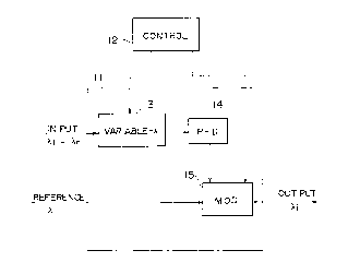
FIG. 3 shows the general construction of the
wavelength-synchronized optical processing device according to
a first ernbodirnent of the present invent ion . The opt ical
processing device of FIG.3 j.s an optical demultiplexer that
9c
27879-94
2059074
selectively recovers an optical signal component from a
wavelength-multiplex optical signal modulated on an input
optical beam, in response to a reference optical beam that
specifies the wavelength of the optical signal to be
recovered.
Referring to FIG. 3, the optical processing device
includes an optic,sl processing unit 11 and a control unit 12,
wherein the optic~31 processing unit 11 is generally formed
from a variable-wavelength band pass filter 13, a
photodetector 14 ~3nd an optical modulation unit 15. The band
pass filter 13 of the optical processing unit 11 is supplied
with an incident ~~pt ical bearn and cont rolled by the cont rol
unit 12 such that only the optical signal that has a
particular wavelength specified by the control unit 12 is
passed through th~= filter 13.
The out~~ut optical beam of the filter 13 is supplied
to the photodetector 14 wherein the photodetector 14 converts
the optical beam 'to an electric
9d
27879-94
- to - 20590 7 4
1 signal. The output electric signal of the photodetec-
tor 14 is supplied to the optical modulation unit 15
and the optical modulation unit 15 modulates the refer-
ence optical beam in response to the electric output of
the photo~detector 14. As will be described later in
detail, the filter 13 may be formed of a DFB laser
amplifier and changes the wavelength of the optical
beam passing therethrough in response to a bias current
that is controlled below the threshold of laser oscil-
lation. 'The optical modulation unit 15 may be a Franz-
Keldysh effect device or a laser diode of which gain
can be changed in response to the output of the pho-
todetector 14.
In operation, an input optical beam that
carries thereon optical signals having respective
wavelengths /~1' - /1n' in the wavelength-multiplex mode
is supplied to the filter 13 that in turn is controlled
by the control unit 12 to pass the optical signal
having th~a wavelength /1i' selectively. Meanwhile, the
wavelength of the reference beam is well stabilized by
using a stabilized optical source such as a laser diode
of which operational temperature and bias current are
compensated for with respect to any variation. There-
by, one obtains the output optical signal from the
optical modulation unit 15 with the wavelength Eli in
correspondence to foregoing original optical signal of
the wavelength Vii'. The circuit 11 can be formed as an
integrated circuit including the control unit 12.
FIG.~~ shows the construction of the filter 13
used in the system of FIG.3.
Referring to FIG.4, the filter 13 includes a
number of filter elements 131 - 134 respectively pass-
ing the optical beams of the wavelengths ~ a - ~Id, as
well as a number of filter elements 135 - 138 respec-
tively passing the optical beams of the wavelengths
~1~ - ~4~~ wherein the wavelength-multiplexed input
optical beam is supplied to each of the filter elements
2050 7 4
- 11 -
1 135 - 138 parallel with each other. Further, the
reference optical beam is supplied parallel to each of
the filter elements 131 - 134.
The output optical beams of the filter ele-
5 ments 135 - 138 are supplied to corresponding variable
transmittance controllers 139 - 1312 each having a
transmitt~ance that is controlled in response to the
output of the corresponding filter element. Thus, when
the reference optical beam is given with the wavelength
10 of Vila, the transmittance of the controller 139 is
selectively increased and the optical signal having the
wavelengtlh /11' and passed through the filter element
135 is selectively outputted as an output optical beam
of the filter 13.
15 In the present embodiment, one may employ any
of the mu:lti-layered dielectric films, optical wave-
guides, o:r the spatial filters that use the diffraction
grating, :Eor the filter element 135 - 139. Preferably,
the wavelE:ngths ~Ia, alb, /lc and /~d may be set coincident
20 to the wavelengths T1', /~2', ~3' and 714' such that ~a
- ~1 ~ ~ ~b = ~2 ~ ~ ~c = ~3 ~ and ~d = ~4' . This, of
course, i:~ not the essential requirement for the opera-
tion of the device.
FIG.~i shows an example of the variable trans-
25 mittance controllers 139 - 1312, wherein the input
optical signal from the filter 135 - 139 is supplied to
a laser amplifier 1323 for amplification by the stimu-
lated emission caused therein in response to the pas-
sage of the wavefront of the input optical beam. The
30 operation of the laser amplifier 1323 is controlled by
an electronic control circuit 1322 that in turn is
controlled in response to an electric signal produced
by a photodetector 1321 to which the reference optical
beam is supplied.
35 More specifically, the electronic circuit
1322 produces a bias signal to the laser amplifier 1323
when therE: is an incident reference optical beam to the
- 12 - 20 590 7 4
1 photodetector 1321. In response to the bias signal,
the laser amplifier 1322 amplifies the incident input
optical signal, while when there is no bias signal, the
laser amplifier 1322 absorbs the input optical signal.
5 For the variable transmittance controllers, one may
use, in addition to the foregoing laser amplifier, a
Franz-Keldysh effect device or MQW optical modulator
that uses the quantum confinement Stark effect.
FIG.6 shows another embodiment of the varia-
10 ble-wavelength filter 13 wherein there is provided an
optical switch 1331 that has a first input port A for
receiving the reference optical beam and a second input
port B for receiving the input optical beam, wherein
one of the optical beams at the input port A and the
15 input port B is supplied selectively to a filter device
1332 of which wavelength is controlled by a controller
1334. The optical beam that has passed through the
filter device 1332 is supplied to a second optical
switch 1333 that has a first output port C connected to
20 an output waveguide (not shown) and a second output
port D connected to the controller 1334.
In operation, the first optical switch 1331
is set at first such that the input port B is selected.
Further, the second optical switch 1333 is set such
25 that the output port D is selected. In this state, the
reference optical beam supplied to the input port B is
transferr~ad to the controller 1334 after passing
through tlhe filter device 1332 and the switch 1333'
Thereby, 'the controller 1334 sets the state of the
30 filter de~~ice 1332 such that the transmittance of the
optical b~aam becomes maximum. After such a training of
the filter device 1332 is completed, the state of the
optical switches 1331 and 1333 switched such that the
input optical beam at the port A is outputted at the
35 port C after passing through the filter device 1332.
Thereby, only the optical signal that has the wave-
length coincident to the wavelength of the filter
20~~p~~
- 13 -
1 device 1332 alone appears at the output port C. In
other words, the system 13 acts as the variable-
wavelengt:h filter that passes the optical signal having
a wavelength coincident to the wavelength of the refer-
s ence optical beam selectively.
FIG.'7 shows the construction of the filter
device 1332.
Referring to FIG.7, the filter device 1332 is
formed of a DFB laser diode that has an active layer
10 1341 and a diffraction grating 1342. In operation, the
device is biased below the threshold of laser oscilla-
tion. Thereby, the incident optical beam causes a
stimulated emission in the active layer 1341 upon
passage tlzerethrough.
15 FIG.B shows the band-pass characteristics of
the laser amplifier of FIG.7 for different bias volt-
ages. As can be seen in FIG.8, the peak of the trans-
mittance ;shifts in response to the bias voltage. By
using thi:~ effect, one can set the pass-band or pass-
20 wavelength in the filter device by means of the con-
troller 1:343.
Acco:cding to the construction of FIG.6, one
can maintain the stable operational characteristics for
the filter 13 as a whole even when there is a change in
25 the operai~ional characteristics of the laser amplifier
itself. Obviously, this is due to the feedback control
of the la:~er amplifier 1332 as described above. For
the optical switches 1331 and 1333, one may use the
direction~~l coupler and saturable optical absorption
30 switch that changes the transmittance in response to
the injection of carriers.
FIG.~l shows a wavelength-synchronized optical
processing device according to a second embodiment of
the present invention.
35 Referring to FIG.9, the device includes an
optical processing unit lla and a control unit llb,
wherein the optical processing unit lla uses the pho-
2o~9a~4
- 14 -
1 todetecto:c 14 for detecting the input optical beam that
has the wavelength of ai' similarly to the optical
processin~~ unit 11 of the first embodiment. This input
optical beam may have the fluctuation in the wavelength
Vii'.
The output electric signal of the photodetec-
tor 14 is supplied to the optical modulator 15 that in
turn is supplied with the reference optical beam of the
wavelengt)a Eli. Thereby, the optical modulator 15 modu-
10 lates the reference optical beam with the output elec-
tric signal of the photodetector 14, and an output
optical beam carrying the optical signal of the origi-
nal wavelE~ngth Vii' is obtained with a stabilized wave-
length of /1i. Further, a control unit 12a is used for
15 controlling the operation of the optical modulator 15.
FIG.:LO shows a wavelength-synchronized opti-
cal proce:asing device according to a third embodiment
of the prEaent invention.
Referring to FIG.10, the optical processing
20 device is formed of an optical processing unit llb and
a control unit 12b, wherein there is provided a laser
diode 16 i~hat is controlled by a controller 12b.
There, thE~ laser diode is injected with the reference
optical bE~am of the stabilized wavelength ~ and fur-
25 ther with the input optical beam of the wavelength 71i'
for producing an output optical beam carrying thereon
the inforrnation modulated on the input optical beam,
with the wavelength of /~i. Thereby, the laser diode
acts as the wavelength converter. Again, the optical
30 signal of the wavelength Vii' and containing fluctuation
is converi:ed to the optical signal of the wavelength ~1i
that is free from fluctuation.
FIG.7.1 shows a fourth embodiment of the
optical processing device according to the present
35 invention.
Referring to FIG.11, the optical processing
device of the present embodiment has a construction
2459074
- 15 -
1 similar to that of FIG.3 except that there is provided
a wavelength converter 17 after the optical processing
unit 11 for converting the wavelength of the output
optical beam from the wavelength /~i to another wave-
s length >1k. By using the optical processing unit lla or
llb described with reference to FIGS.9 and 10 for the
wavelength converter 17, one can obtain the output
optical beam with the stabilized wavelength ~k.
FIG.12 sh~~ws the optical processing device accord-
ing to a fifth embodiment of the present invention.
Referring to the drawing, the optical proc-
essing device of the present embodiment has a structure
similar to that of FIG.10 except that there is provided
a variable-wavelength filter 18 provided for filtering
the input optical beam. As shown in FIG.12, the varia-
ble-wavelength filter 18 is controlled by the control-
ler 12b and selectively passes one of the optical
signals multiplexed on the input optical beam with the
wavelengtlhs'11' - an' . In this case, too, any of the
desired optical signals that are multiplexed on the
input optical beam with the wavelength-multiplex mode
is converted to the desired, stabilized wavelength ai.
FIG.:L3 shows an optical path selector accord-
ing to a ;sixth embodiment of the present invention,
wherein a number of optical processing devices 211 -
21n are u:~ed.
Referring to the drawing, the optical path
selector of the present embodiment uses a number of
electro-optic converters 231 - 23n, wherein each elec-
tro-optic converter may be formed from a laser diode
that produces an optical signal with a wavelength that
is pertinE;nt to the laser diode. Thus, the electro-
optic converter 231 produces the optical signal with a
wavelength al, the electro-optic converter 232 produces
the optic<31 signal with a wavelength ~2, . . . , and
the electro-optic converter 23n produces the optical
signal wii~h a wavelength Vin. Further, the output
- 16 - 20 590 7 4
1 optical signals of these electro-optic converters are
supplied to an optical synthesis and distribution unit
24 that synthesizes a wavelength-multiplex optical
signal from these optical signals.
The output optical signals thus produced by
the unit 24 are supplied to respective optical process-
ing devices 211 - 21n, wherein each optical processing
device 211 - 21n has a construction similar to any of
the wavelength-synchronized optical processing devices
described previously. Further, there is provided a
reference optical beam generator 22 that includes a
number of stabilized laser diodes each stabilized in
terms of the temperature and bias current and produces
the reference optical beam with stabilized wavelengths.
The reference optical beam thus produced is
supplied to the optical processing devices 211 - 21n as
the reference optical beam as described previously, and
each optical processing device produces an output
optical beam with the stabilized wavelength that is
specified by the wavelength of the reference optical
beam. Thnss, when the reference optical beam having the
wavelength /~1 is supplied to the optical processing
device 211, the original optical signal having the
wavelengtlh /11 is selectively outputted to the optical
transmission line connected to the optical processing
device 211 with the stabilized wavelength of X11.
Alternati~~ely, the optical processing device 211 may be
supplied with the optical output signal of the wave-
length X12 from the electro-optic converter 232 and
output the same on the transmission line connected to
the device 211 with the wavelength of ~1. The
selection of the wavelength of the input optical signal
at the opitical processing device 211 - 21n may be
achieved by the control unit provided in each of the
optical processing device.
Hy multiplexing the output optical signals of
the optical processing devices 211 - 21n again, one can
_ 1~ _ 2459074
1 obtain a wavelength-multiplexed optical signal wherein
the wavelength of each signal component is highly
stabilized even when there is a fluctuation in the
oscillation wavelength of the laser diode used in the
5 electro-optic converters 231 - 23n. Thus, the system
of the present embodiment is suited for use in optical
path selectors or optical transmitters that send the
wavelength-multiplex optical signals with stabilized
wave 1 engt'hs .
10 FIG.14 shows the block diagram of an optical
transmitt~ar according to a seventh embodiment of the
present invention.
Referring to FIG.14, there are provided a
number of electro-optic converters wherein the electro-
15 optic con~~erters are grouped into a number of groups
each including the electro-optic converters 231 - 23n.
In each group, the output optical beams produced by
these electro-optic converters are supplied to corre-
sponding optical processing devices 211 - 21n directly
20 similar to the embodiment of FIG.14. Further, the
reference optical beam generator 22 produces the refer-
ence optical beams with the wavelengths of 711,
~2, . . ~, ~1n similar to the embodiment of FIG.13.
Thereby, i~he wavelengths ~1 - 71n are changed from each
25 other in Each group while the reference optical beams
are supplied to the optical processing devices of other
groups in parallel.
In operation, the optical processing device
can produce the optical signals with any desired wave-
30 lengths by supplying thereto suitable reference optical
beams fronn the generator 22. For example, one can
obtain thE~ output optical signal from the device 211 by
supplying the reference optical beam thereto with the
wavelength of '1n. Thus, the present embodiment is
35 useful for the optical transmitters and the optical
repeaters.. Further, the system of FIG.14 can be con-
figured to form a number of optical channels each
2059074
- 18 -
1 carrying 'the wavelength-multiplexed optical signals of
the wavelengths of ~11 - /fin.
FIG.15 shows an optical matrix switch accord-
ing to an eighth embodiment of the present invention,
wherein there are provided a number of optical trans-
mission lanes 33 at the input side and a number of
optical t:cansmission lines 34 at the output side. On
each tran:~mission line 33 of the input side, wave-
length-multiplexed optical signals are supplied with
wavelengths '11' - ~', while on each transmission line
34 of the output side, wavelength-multiplexed optical
signals a:re carried with wavelengths of al - ~n~
At each intersection of the transmission line
33 and the transmission line 34, there is provided a
wavelength-synchronized optical processing device 31
that has a construction of any of the foregoing embodi-
ments of 1~IGS.3 - 12, and each optical processing
system 31 is supplied with the reference optical beam
that is produced by a reference optical beam generator
32 with the stabilized wavelengths of ~1 - ~ n. There-
by, the optical processing device 31 causes a transfer
of the input optical signal of the selected wavelength
from the i~ransmission line 33 of the input side to the
optical t~_ansmission line 34 of the output side, where-
in the opi:ical signal thus transferred has a stabilized
wavelength that is specified by the wavelength of the
reference optical beam.
It should be noted that each optical trans-
mission l~lne 34 carries thereon a number of wavelength
multiplexE:d optical signals produced by a group of the
optical processing devices 31 that are connected com-
monly to a single optical transmission line 33. Par-
ticularly, the group of the optical processing devices
31 that are provided commonly on one optical transmis-
sion line 33 are supplied with a single reference
optical bE:am commonly, and the wavelength of the refer-
ence optical beam is changed in each optical transmis-
~45907~ ,
_ lg _
1 sion line 33. Thereby, optical signals of different
wavelengths are outputted on each optical transmission
line 34 of the output side. Further, by changing the
combination of the wavelengths of the reference optical
beams on 'the lines 34, one can output any optical
signal on any optical transmission line 33 on any
desired optical transmission line 34 with any desired
wavelength.
FIG.16 shows the details of the optical
matrix switch of FIG.15.
Refe:cring to FIG.16, there is provided an
optical divider 35 on the optical transmission line in
correspondence to each of the optical processing de-
vices 31 for tapping the wavelength-multiplexed optical
signals on the transmission line 33, and the optical
signals thus tapped are supplied to the optical proc-
essing de~~ice 31. The optical processing device 31
selects one of the optical signals on the line 33 and
outputs the selected optical signal with the wavelength
of the re:Eerence optical beam. The output optical beam
of the optical processing device 31 in turn is supplied
to an optical coupler 36 that is provided on the opti-
cal transmission line 34 in correspondence to each of
the optical processing device 31. The optical coupler
36 establishes an optical coupling between an optical
fiber or waveguide that carries the optical output of
the system 31 and the optical fiber or waveguide form-
ing the optical transmission line 34, and the optical
beam outputted from the optical processing device 31 is
merged or wavelength-multiplexed upon the optical
signals on the line 34. It should be noted that such
an optica:L matrix switch can be constructed in the form
of optical integrated circuit by forming the optical
divider 3'.5 and the optical coupler 36 together with the
optical processing device 31 and the reference optical
beam generator 32 on a common substrate.
FIG.:l7 shows an optical matrix switch accord-
2059074
- 20 -
1 ing to a :ninth embodiment of the present invention.
Referring to FIG.17, two optical matrix
switches 38 and 39 each having the construction of
FIG.16 are connected in series, wherein the matrix
5 switches 38 and the matrix switches 39 are connected by
intermediate optical transmission lines 371 - 37n.
These optical transmission lines act as the optical
transmission lines at the output side for the optical
matrix switch 38 while act simultaneously as the input
10 side optical transmission lines for the optical matrix
switch 39. Further, the reference optical beam genera-
tor 32 is used commonly for both the optical matrix
switch 38 and the optical matrix switch 39, wherein the
reference optical beam generator 32 supplies the refer-
15 ence optical beams to the optical matrix 38 and the
optical matrix 39 independently.
In the typical example of operation, the
reference optical beam having the wavelength of ~1 is
supplied to a group of the optical processing devices
20 31 that ace located at the intersections formed between
the line :331 and the lines 371 - 37n, while the refer-
ence optical beam having the wavelength of ~2 is sup-
plied to another group of the optical processing de-
vices 31 i~hat are located at the intersections formed
25 between the line 332 and the lines 371 - 37n. Similar-
ly, the wavelength of the reference optical beam sup-
plied to a group of the optical processing devices 31
that are provided on a common optical transmission line
of the input side is changed with respect to the wave-
30 length of the reference optical beam that is supplied
to the to another group of the optical processing
devices 3~L that are provided commonly on another input
side optical transmission line. Thereby, the overlap-
ping of the wavelength of the optical signals that are
35 outputted commonly on an output side optical transmis-
sion line such as the line 371 is positively eliminat-
ed.
2059074
- 21 -
1 The optical signals thus outputted on the
lines 371 - 37n are then switched by the second optical
matrix switch 39, wherein the optical switching similar
to the one described with reference to the optical
5 matrix switch 38 is achieved. Thereby, output optical
signals having respective wavelengths determined by the
wavelength of the reference optical beams supplied to
the optical matrix switch 39 are obtained at the output
optical transmission lines 341 - 34n. The wavelength
10 of these output optical signals is of course stabilized
by using the stabilized optical source for the refer-
ence optical beam generator 32.
FIG.18 shows a tenth embodiment of the
present invention, wherein the present embodiment forms
15 a wavelength converter for converting the wavelength of
the optical signals modulated on the input optical beam
with the 'wavelength-multiplex mode and outputting the
optical signals thus converted in the wavelength multi-
plex mode.
20 Referring to FIG.18, there are provided a
number of optical processing devices 411 - 41n each
having the construction of any of the wavelength-
synchronized optical processing devices described
previously, wherein each of the optical processing
25 devices 411 - 41n is supplied with the wavelength-
multiplex optical signals from the optical distribution
part 44 that in turn is supplied with an input optical
beam carrying the wavelength-multiplex signals and
distributing the same to the optical processing devices
30 411 - 41n. Further, the optical processing devices 411
- 41n are controlled by a control unit 43 that selects
an optical signal from the wavelength-multiplexed
optical signals. When the optical processing unit 11
is used for the optical processing devices 411 - 41n,
35 the control unit 43 controls a variable-wavelength
filter similar to the filter 13 of FIG.3. Thereby, the
control unit 43 acts as the control unit 12.
22 _ 20 590 7 4 ~'
1 Further, there is provided a reference opti-
cal beam generator 42 that produces the reference
optical beam with the wavelengths al, ~2, . . ., /~ n
and supply the same to respective optical processing
5 devices. In response to the reference optical beams
thus supplied, the optical processing devices 411 - 41n
produce output optical beams in coincidence with re-
spective wavelengths of the reference optical beams.
The output optical beams thus produced are added in an
10 optical s:~nthesis unit 45 that produces the an output
optical beam on which the optical signals are modulated
in the wa~~elength-multiplex mode.
In the system of the present embodiment, it
should be noted that one can convert the optical signal
15 of the wavelength /1i to the optical signal having the
stabilized wavelength ~~. For example, one can convert
the optic~~l signal of the wavelength 11 to the optical
signal of the wavelength n and the optical signal of
the wavelength /12 to the optical signal of the wave-
20 length ~l1 "
FIG.:L9 shows an eleventh embodiment of the
present invention.
Referring to FIG.19, the optical processing
system of the present embodiment includes a number of
25 wavelength-synchronized optical processing devices 5111
- 51~ described previously with reference to FIGS.3 -
12 and a ~_eference optical beam generator 52 for pro-
ducing thE: reference optical beam.
In tree present embodiment, there are a number
30 of optical. transmission lines 531 - 53m at the input
side, wherein each transmission line is connected to a
corresponding optical distribution unit 551 - 55m and
supplies thereto a wavelength-multiplexed input optical
beam. Similarly to previous cases, the input optical
35 beam carries thereon the optical signals of the wave-
lengths /~~_ ' - /~n' .
Each optical distribution unit such as the
-23- 205907 '~'
1 unit 551 is connected to a number of optical processing
devices such as 5111 - 511n for supplying the wave-
length-multiplexed optical signals to each of these
devices. The optical processing devices are supplied
5 with the :reference optical beams from the reference
optical beam generator 52 with selected wavelengths and
produce tlhe output optical signals with the wavelength
specified by the wavelength of the reference beams.
More particularly, the reference optical beam
of the wavelength ~1 is supplied to the optical proc-
essing devices 5111 - 511n commonly, the reference
optical beam of the wavelength a2 is supplied to the
optical processing devices 5121 - 512n (not shown)
commonly, . . . and the reference optical beam of the
15 wavelength '1n is supplied to the optical processing
devices S:Lml - 51 mm, commonly. Thereby, all the output
optical signals produced from the optical processing
devices 5:L11 - 511n have the wavelength al, all the
output opi~ical signals produced from the optical proc-
essing devices 5121 - 512n have the wavelength
)12, . . ., and all the output optical signals from the
optical p~.ocessing devices 5lml - 51~ have the wave-
length of ~ln.
In the present embodiment, the optical output
of each optical processing device is supplied to a
corresponding optical synthesis unit such that each
optical s5rnthesis unit is supplied with optical signals
of mutual~Ly different wavelengths from different opti-
cal processing devices. For example, the output opti-
30 cal signal. of the optical processing device 5111 is
supplied t:o an optical synthesis unit 561, the optical
output of the optical processing device 5112 is sup-
plied to an optical synthesis unit 562 (not
shown) . ., . and the optical output of the optical
35 processing device 511n is supplied to an optical syn-
thesis unit 56m. It should be noted that all the
optical output signals mentioned above have the wave-
2059074
- 24 -
1 length of X11.
When viewed from the side of the optical
synthesis unit, the optical synthesis unit 561 is
supplied with the output optical signals from the
5 optical processing devices 5111, 5121, . . . 5lml with
the wavelengths of X11, /12, . . . /'jn and produces an
output optical beam on which these optical signals are
multiplexed in the wavelength-multiplex mode. Similar-
ly, the opticai synthesis unit 56m is supplied with the
10 output optical signals from the optical processing
devices 511n, 512n, . . . 51~ with respective wave-
lengths of X11, X12 , . . . a n and produces an output
optical beam on which the optical signals are multi-
plexes in the wavelength-multiplex mode. Thereby, the
15 system of FIG.19 converts the wavelength of the optical
signals from ~11' - an' to ~l - an and simultaneously
stabilizes the wavelength of the output optical sig-
nals. It should be noted that any combination of the
optical signals supplied on the input side optical
20 transmission lines 531 - 53m can be obtained on each of
the output side transmission lines 541 - 54m in the
form of wavelength-multiplexed optical signals.
FIG.:~O is a block diagram showing the con-
struction of an optical information transmission system
25 wherein an optical matrix switch 61 having the con-
struction of FIG.15 or FIG.17 is used.
Refeo~ring to FIG.20, there are provided a
number of optical transmission terminals 621 - 62m
connected to the input side optical transmission lines
30 of the opi~ical matrix switch 61. Further, a number of
optical rE~ception terminals 631 - 63m are connected to
the outpui~ side optical transmission lines of the
matrix swatch 61.
Each optical transmission terminal such as
35 the terminal 621 includes an optical transmitter 64 for
producing a number of optical signals with respective
wavelengths ~11 - ~n and an optical synthesizing unit 65
2059074
- 25 -
1 supplied with the optical signals for producing a
wavelength-multiplexed optical beam from the optical
signals. On the other hand, each optical reception
terminal ouch as the terminal 631 includes an optical
distribution unit 66 supplied with the wavelength-
multiplex~~d optical signals from the optical matrix
switch 61 and a variable-wavelength filter 67 for
selecting an optical signal of a specific wavelength.
Further, 'there is provided a photodetector 68 in con-
nection with the filter 67 for detecting the optical
signal th~~a has passed through the filter 67.
Hy controlling the optical matrix switch 61
in accordance with control information such as the
address information, the path and the wavelength of the
optical signals are switched in the matrix switch 61.
More specifically, one can switch a huge number of
channels ;number of wavelength multiplex signals X
number of transmission lines) simultaneously by using
the system of FIG.20.
FIG.:?1 shows a thirteenth embodiment of the
present invention.
Referring to FIG.21, the system of the
present embodiment is also an optical transmission
system, wherein there are provided a number of trans-
mission tE:rminals 731 - 73m each supplied with electric
signals and producing optical signals in correspondence
to the elE:ctric signals with respective wavelengths.
The output optical signals of the terminals
731 - 73m are supplied to an optical path selector 71
that includes a number of optical synthesis and distri-
bution units 75 as well as 76 provided in correspond-
ence to the transmission terminals 731 - 73m and the
reception terminals 741 - 74m. The optical path selec-
tor 71 ha:~ a construction similar to the system shown
in FIG.19, and the output optical signals of each
transmiss9.on terminal are mixed to form a wavelength-
multiplexE~d optical signal similar to the embodiment of
- 26 - ~05907t~ .
1 FIG.19. 1~urther these wavelength-multiplexed optical
signals a:re selected by the optical processing devices
similar to the devices of 5111 - 51~ and are distrib-
uted further to a number of optical synthesis and
distribution units 76 provided in correspondence to the
optical reception terminals 741 - 74m. In FIG.21, the
optical processing devices are not illustrated for the
sake of c:Larity of the drawing. There, any combination
of the opi~ical signals produced by the optical trans-
mission tE:rminals 731 - 73m is obtained at the output
of each optical synthesis and distribution unit 76 in
the form of the wavelength-multiplexed optical signals.
The optical output thus obtained is then
selective7Ly passes through a filter 77 and detected by
a photodet:ector 78. In this case, too, one can switch
a large number of connections of which number is given
by the product of the number of wavelength-multiplex
signals acid the number of optical transmission lines or
channels, simultaneously.
Further, the present invention is not limited
to the emt~odiments described heretofore, but various
variation:> and modifications may be made without de-
parting from the scope of the invention.
30