Note: Descriptions are shown in the official language in which they were submitted.
JA9~ 003
; LCD C~NTR~LI.ER, LCD ~PP~RATUS, ~ND INFORM~TION
P~C~5SING ~PPAR~'~U~
The present invention relates -to a LCD apparatus, and more
particularly to a method for clriving a LCD panel. The
general subject matter relating Io the present invention,
together with the lnvention itself, will be clearly
understandable from the following description taken in
conjunction with the appended drawings, wherein:
FIG.l shows waveform charts of control signals in an
embodiment of a LCD controller according to the present
invention.
FIG.2 is a block diagram showing an embodimen-t of a LCD
apparatus constructed in accordance with the present
invention.
FIG.3 is a block diagram showing an embodiment of an
information processing apparatus constructed in accordance
with the present invention.
FIG.4 shows waveform charts of control signals in a
conventional LCD controller.
FIG.4 shows display control signals and display data in a
conventional LCD apparatus. In the figure, a frame pulse FP
and a latch pulse correspond to a vertical synchronizing
signal and a horizontal synchronizing signal for a display
controller, respectively. A shift clock pulse SCP is a
clock signal for data transfer and a data stored in a shift
register for signal electrodes shifts each time the shift
clock pulse SCP is provided to the shift register. From the
shift register for the signal electrodes, data is
transferred in parallel to a driver output stage for the
signal electrodes each time -the latch pulse LP is provided
to the shift register. Said signal driver output stage
outputs a potential which is corresponding to the data to a
signal electrode. The latch pulse LP is provided at the
same time not only to the shift register for the signal
electrodes, but also to a shift register for scarming
J~9--91-003 2
elec-trodes. Each time the la-tch pulse LP :is provided to the
shift register for the scanning electrodes, -the frame pulse
FP is shifted as da-ta within the shift register for the
scanning electrodes and -thus the scanning electrodes are
seguentially turned on each time the latch pulse LP is
provided to the shift register for -the scanning electrodes.
As a result, the scanning electrodes are turned on one after
another simultaneously with the output of a data signal to
the signal electrodes, that is, the disp.Lay operations of
display lines change one after another.
A vertical blanking -term is established between frames.
Immediately aftar the frame pulse FP is shifted to a
scanning electrode for the last display line and the
scanning electrode for the last display line has been turned
on, the following frame pulse FP does not generate, but do
at a predetermined interval and thus the vertical blanking
term is established. That is, the scanning electrode for
the last display line is turned on and then, at the
predetermined interval, a scanning electrode for the first
display line of the following frame is turned on to
establish the vertical blanking term. However, in such a
conventional LCD apparatus, it became clear that the effec-t
of data for the last display line appeared in the first
display line in some cases. The inventor et al.
investigated a cause of such phenomenon. That is, in a
conventional LCD apparatus, even during a vertical blanking
term after the last display line has been displayed, the
application of a potential according to data for the last
display line to a signal electrode remains continued.
However, any scanning electrode being not turned on during
the vertical blanking term, any display line is not in a
display state, regardless of the potential of the signal
electrode. As shown above, even though a potential
according to data for the last display line is applied to
the signal electrode for a long period of time and then a
potential according to data for the first display line of
the following frame is applied to the signal electrode, the
voltage applied to the signal electrode does not immediately
change accordingly.
IIJ '1~ 3 . ~ '
JAg-91-003 3
In a LCD apparatus usiny a two-sp].itted driving method,
constructed so tha-t the upper half and the lower half areas
on one LCD panel are driven by different columns of signal
electrodes, the first display line of -the lower area being
in the middle of the LCD panel, the phenomenon described
above remarkably appears. In particular, if a pattern in
which only one horizontal line is displayed at the bottom of
the lower area and none of lines is displayed in other
areas, is to be displayed, the horizontal line appears in
the middle of the screen, that is, in the first display line
on the lower half screen. Ln a LCD apparatus in multiple
display modes in which -the number of display lines is
different from one ano-ther, if the display area includes
only the number of partial display lines smaller than that
of display lines which can be displayed, a LCD controller
blanks out margins at the top and the bottom of the screen
(fixes at either on or off level) due to the centering of
the display area. In this case, if reversed display is
present in the middle of the screen, as expected, the
horizontal line appears in the middle of the screen (in the
first line on the lower screen).
A driver for the signal electrodes of the lower screen is
arranged under columns of the signal electrodes and the
display lines are usually driven so that they move from the
top to the bottom of the screen. Therefore, the first
display line of the lower screen is arranged at the longest
distance from a driver output stage for the signal
electrodes. This causes an impedance from the driver output
stage to the first display line for the signal electrodes to
increase and it becomes difficult that a potential
corresponding to the first display line changes rapidly.
Also in this respect, the phenomenon shown above becomes apt
to occur.
An object of the present invention is to remove the effect
of data for the last display line on the first display line.
In the present invention, prior to a horizontal duration
immediately before scanning electrodes for the first display
line of the following frame are turned on after the
JA9-91-003 4
completion of the last display of the scanning electrodes,
signal elec-trodes are pre-charged with an electric po-ten-tial
according to data for the first line of said following frame
to accomplish said objec-t. That is, in the present
invention, an electric potential according to data for said
first display line is applied, earlier than done in a prior
art, to the sig~al electrodes, to give the signal electrodes
sufficient time to change to the potential accordiny to data
for the first display line and thus said object is
accomplished.
~ ~ .
In the following, an embodiment o~ the present invention is
described by reference to drawings.
FIG.3 shows an embodiment of an information processing
apparatus constructed in accordance with the present
inven-tion. In the figure, to a bus 3 of a CPU 1, a screen
memory 5 and a display controller 7 are connected and to the
display controller 7, a LCD module 9 is connected. The
screen memory 5 stores a picture image data to be displayed
by a LCD cell 10 (Refer to FIG.2) in the LCD module 9 and
the picture image data is rewrit-ten by the CPU 1. The
display controller 7 transfers the picture image data stored
in the screen memory 5 and each signal for display control
shown in FIG.l together to the LCD module 9.
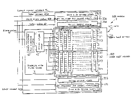
As shown in FIG.2, the LC~ module 9 comprises a matrix-type
- LCD cell 10 and a liquid crystal driver 15. The LCD cell 10
driven by a two-splitted driving method, includes columns of
signal electrodes (may be called da-ta electrodes or segment
electrodes) Yl, Y2, Y3, ... YI1 and rows of scanning
electrodes (may be called common electrodes) ~1, X2, X3, ...
Xm for an upper half screen lOA and a lower half screen lOB.
The liquid crystal driver 15 includes data side driver
blocks 17A and 17B and a scanning side driver block 19. The
data side driver blocks 17A and 17B include driver output
stages 20A and ~OB and shift registers 30A and 30B for the
signal electrodes, respectively. The scanning driver block
19 includes a shift register 40 for the scanning electrodes
and a driver output stage 45. Each of the columns of signal
electrodes Yl, Y2, Y3, ... Yn for the upper half screen and
JA9-91-003 5
the lower half screen is connec-ted to the driver OUtpllt
stages 20A and ~OB, respec-tively. The driver outpu-t stayes
20A and 20B are connec-ted to the shift reyisters 30A and 30B
for the signal electrodes, respectively. The respective
scanning electrodes Xl, X2, X3, ... Xm for the upper and the
lower screens lOA ancl lOB are connected to the common shift
regis-ter 40 for the scanniny electrodes.
In the following, the operations of the embodi~ent are
described by reference to FIG.1 in addition to FIG.2 an~
FIG.3.
The display controller '7 divides data signals for display
into two groups of the upper and the lower screens and
transfers them to the li~uid crystal driver 15. A data
signal for the upper screen and a data signal for the lower
screen synchronize with a shift clock pulse SCP and shift
into the shift registers 30A and 30B for the signal
electrodes for the upper and the lower screens lOA and lOB,
respectively. After the completion of -the shift of data
corresponding to all signal electrodes ~ 2, Y3, ... Yn
for one display line into the shift registers 30A and 30B
for the signal electrodes, the data is transferred to the
driver output stages 20A and 20B by means of a latch pulse
LP and the driver output stages 20A and 20B synchronize with
the latch pulse LP and simultaneously output an elec-tric
potential according to the data for one display line
corresponding to all signal electrodes Y1, Y2) Y3, ... Yn.
The latch pulse LP is inputted simultaneously not only to
the driver output stages 20A and 20B, but also to a clock
input of the shift register 40 for the scanning electrodes.
A frame pulse FP is inputted to a data input of the shift
register 40 for the scanning electrodes and shifted within
the shift register 40 for the scanning electrodes each time
a la-tch pulse LP is inputted. Thus, by means of a first
latch pulse LP after a rise of a frame pulse FP, a first
scanning electrode X1 (scanning electrode for a first
display line) is turned on by the driver output stage 45,
then by means of a second latch pulse LP, a second scanning
electrode X2 is turned on, and finally a scanning electrode
JA9-91--003 6
Xm, -the same as above, ls turned on. Tha-t is, the scanning
electrodes Xl, X2, ~3, ... ~m are sequentially turned on
synchronously with latch pulses LP. In other words, each
time data for one display line is se~uentially transferred
to one of -the signal electrodes Yl to Yn by means of a latch
pulse LP inputted to clock inputs of the shift registers 30A
and 30B for the signal electrodes, the respectlve scanniny
electrodes Xl, X2, X3, ... Xm of the upper and the lower
screens lO~ and lOB are se~uentially turned on by means of
latch pulses LP inputte~ -to the clock input of the shift
register ~0 for the scanning electrodes.
In the followiny, the lower screen lOB is mainly described,
but unless otherwise specified, the same description holds
true for the upper screen lOA.
At the completion of the transfer of data for the last
display lins (scanning electrode Xm) to the shift register
30B, by the shift latch pulse LP, an electric potential
corresponding to the data for the last display line is
applied to the signal electrodes Yl to Yn from the driver
output stage 20B and the scanning electrode Xm is turned on.
As a result, the last display line is displayed. Also after
the last display line has been displayed, latch pulses LP
are transmitted one after another at the time interval of a
predetermined horizontal duration from the display
controller 7. However, the following frame pulse FP is not
transmitted from the display controller 7 immediately after
the last display line has been displayed. Accordingly,
until the following frame pulse FP is provided to the
scanning electrode Xl (for the first display line) by means
of a latch pulse LP, any scanning electrodes are not turned
on. This period of time for which any scanning electrodes
do not become on is referred to as a vertical blanking term.
In a conventional LCD apparatus, data for the first display
line of the following frame is transferred to the shift
register for the signal electrodes at a horizontal duration
immediately before the following frame pulse FP and
outputted to the signal electrodes at the next horizontal
duration. However, in the embodiment, at a hori~on-tal
f, .3 ~
JA9-9l.-003 7
duration followed by a hor:izontal dwra-tion immecliately
before a horizontal dura-tion in the conventional LCD
apparatus, data for the Eirst display line of the following
frame is transferred to -the data side driver block 17B or
the shift register 30B for the signal electrodes and at the
next horizontal duration, the data is outputted to the
signal electrodes Yl to Yn. The data transferred to the
shift register 30B is outputted, by means of the first latch
pulse LP after the completion of the transfer of the data,
from the driver output stage 20B in an electric potential
accordance to the data to pre-charge -the signal electrodes
Yl to Yn. At this point, any scanning electrodes Xl to Xm
are not turned on and thus a vertical blankiny term
continues.
When immediately before the completion of a horizontal
duration at which the signal electrodes Yl to Yn are
pre-charged with a potential according to the data for the
first display line, the following frame pulse FP is
transmitted to the shift register 40 for the scanning
electrodes from the display controller 7, the first scanning
electrode Xl is turned on, by means of the first latch pulse
LP after a rise of the frame pulse FP, to display the first
display line. Then a potential according to data for the
second display line (scanning electrode X2~ previously
transferred to the shift register 30A is outputted, by means
of the following latch pulse LP, to the signal electrodes Yl
to Yn to display the second display line. The remaining
display lines are se~uentially displayed in the same manner
as above.
According to the embodiment, a period of time for which a
data signal for the first display line is provided to a
signal electrode, although the period of time corresponds to
one horizontal duration the same as in data signals for
other display lines in the case of the conventional LCD
apparatus, cor:responds to two horizontal durations.
Therefore, before the first scanning electrode Xl is turned
on and the first display line is displayed, the signal
electrodes Yl to Yn is given sufficien-t time required to
change an electric potential in response to new data and
: JA9-91-003 8
thus data for the las-t clisplay l.ine has not an effect on -the
~ first display line.
"
In said embodiment, at a horizontal duration followed by a
horizontal duration immediately before a frame pulse FP,
data for the first display line is transferred to the shift
register 30B for the signal electrodes. However, it will be
appreciated that at the horizontal duration immediately
before the frame pulse FP, the data for the first display
line may be transferred again to the shift register 30B for
the signal electrodes. If the data for the first display
line is transferred to the shift register 30B for the signal
electrodes a-t -the horizontal cluration followed by the
horizontal duration immediately before the frame pulse EP,
whether or not the data for the first display line is
transferred again to the shift register 30B for the signal
electrodes at a horizontal duration immediately before the
following frame pulse FP, an elec-tric potential according to
the data for the first display line is applied to the signal
electrodes Yl to Yn over two horizontal durations.
i
It will be appreciated also that data for the first display
line may be transferred aarlier to the shift register 30B
for tha signal electrodes. For example, it will be
appreciated that at a horizontal duration immediately after
data for the last display line of the preceded frame has
been transferred to the shift register 30B for the signal
electrodes, data for the first display line of the following
frame may be transferred to the shift register 30B for the
signal electrodes to output to a signal electrode.
As described above, the present invention has an advantage
that data for the last display line has not an effect on the
first display line.