Note: Descriptions are shown in the official language in which they were submitted.
2060429
A NETHOD FOR ~EDUCING THE INFLUENCE OF DI8TORTION PRODUCT8
TECHNICAL FIELD
The invention relates to a method for reducing the influence of
distortion products formed in a signal processing system in
conjunction with the analogue-digital conversion of an electric
signal, from which two quadrature signals are formed prior to the
conversion process.
PRIOR ART
When an electric sig~al is to be processed in a system, it is often
desired that signal processing is effected as linearly as
possible. This will avoid the signal being distorted by non-
linear distortion. Examples of signal processing include
analogue-digital conversion, amplification and frequency conver-
sion. Non-linearities of individual components included in a
system are added together and consequently strict demands are
placed on components which are included in large systems on which
the requirement for linearity is high. Such systems are therefore
often relatively expensive. Furthermore, the maximum linearity
of a system is limited by the maximum performance in this respect
of the individual, available components.
It can be mentioned by way of example that one problem which is
liable to arise from non-linear distortion is that an airborne
radar station will sometimes receive an echo from another aircraft
simultaneously with a ground echo. In conjunction with analogue-
digital conversion of the received signals, distortion productsoccur, i.e. harmonics and intermodulation products, such that the
ground echo will give rise to a single large echo and a plurality
of mutually different smaller echoes, unless the conversion is
linear. In turn, this means that the echo from the secand aircraft
cannot always be detected, since a relatively high detection
threshold must be used in order to filter out the smaller echoes
caused by the non-linear conversion.
-
2 2060~29
DISCLOSURE OF THE INVENTION
As indicated in the introduction, the object of the present
invention is to reduce the influence of distortion products that
are formed in conjunction with the analogue-digital conversion of
samples of an electric signal, from which two quadrature signals
are formed prior to said conversion. The desired result is
achieved by phase modulating the quadrature signals prior to said
conversion and by phasedemodulating subsequent to saidconversion
with a value which is changed with each new sample, so that the
energy content of individual distortion products will be spread
out over a relatively broad band. This is made possible by the
fact that only the useful signal, i.e. the fundamental tone, is
correctly demodulated. Sub-harmonics and intermodulation
products, on the other hand, wili have a residual phase modulation
subsequent to said demodulation process.
The characteristic features of the invention are set forth in the
following Claims.
BRIEF DESCRIPTION OF THE DRAWING
The invention will now be described in more detail with reference
to the accompanying drawing, the single Figure of which illust-
rates an exemplifying embodiment of an arrangement for carrying
out the inventive method.
BEST MODE OF CARRYING OUT THE INVENTION
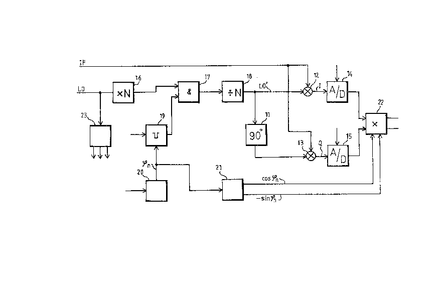
Figure 1 illustrates an exemplifying embodiment of an arrangement
for carrying out the inventive method. An input signal IF which
lies on a carrier frequency LO and a reference signal LO having the
frequency LO are delivered to the arrangement. Two quadrature
signals I and Q in the baseband are formed from the input signal
IF with the aid of a signal LO', a phase-shifting device 11 which
shifts the phase through 90 degrees, and two mixers 12 and 13.
Each of the two quadrature signals is delivered to a respective
analogue-digital-converter 14 and 15. The signal LO' used to form
-- 3 2060~29
the quadrature signals is, in turn, formed by the reference signal
LO in a manner hereinafter described.
The expedient of forming two quadrature signals from a signal
which is to be analogue-digital converted and then to convert each
of the signals to a digital form belongs to the known prior art.
This conversion is carried out in order to enhance the sensitivity
of the system.
In the present example, the signal LO' used to produce the
quadrature signals is formed in the following way. The reference
signal having the frequency LO is delivered to a frequency
multiplying device 16 which forms a signal whose frequency is N
times higher than the frequency of the signal on its input. This
results in a signal of frequency N*LO. This signal passes through
an AND-gate 17 and is then delivered to a frequency divider 18
which divides the incoming frequency by N and thereby generates a
signal having the frequency LO. This signal is designated LO'.
The gate 17, however, is held closed over brief time intervals
with the aid of pulses from a pulse generator 1~ which is control-
led by a random value generator 20. This latter generator
generates random values which are designated ~ . In practice,
these values may, for instance, be determined in accordance with
the formula ~n = m*(2~/N), where m is an integer which can be
varied randomly between 0 and N-1. For instance, when N is equal
to 4~ ~n will thus assume the values 0, ~/2, ~ and 3~/2.
Each random value causes the pulse generator Ig to deliver a stop
pulse to the gate 17, the duration of this pulse being propor-
tional to the random value at that particular time. Because the
signal having the high frequency N*LO is delayed in the gate 17 for
a given period of time, the frequency divider 18 will also be
stopped over the same length of time and thereafter will continue
from the point at which it was interrupted. This results in a time
delay of the divided signal LO', which in practice implies a phase
shift of the signal LO' in relation to the reference signal LO.
By sUitable dimensioning of the components in the pulse generator
19, this means that the quadrature signals I, Q can be phase-
4 2060429
modulated in the form of a phase shift with the value ~ from therandom value generator 20. A new phase shift value ~n is generated
by the random value generator 20 for each new sample of the input
signal IF to be converted to digital form. Thus, the quadrature
signals I, Q are phase-shifted with a new value fox each new sam~le
of the input signal IF.
Reference 23 identifies a time control device which is controlled
by the reference signal LO and which functions to generate signals
for activation of the analogue-digital-converters 14, 15, the
pulse generator 19 and the random value generator 20. These
signals are identified symbolically in the drawing by means of
arrows.
The phase shift value ~n is also delivered to a device 21 which
forms the values cos ~n and -sine ~n from the value ~ , each of
these values being applied to a respective output line. These
values and the digitally-converted samples of the quadrature
signals from the analogue-digital-converters 14, 15 are delivered
to a complex multiplier 22. The quadrature signals from the
converters 14, 15 are decoded, i.e. phase demodulated, in the
comple~ multiplier, by multiplying two complex numbers, of which
one is formed by the quadrature signals and the other is formed by
the values cos ~n and -sine ~n. Decoding corresponds to a phase
shift through the angle ~~n' i.e. a phase shift whose magnitude is
equal to the phase shift effected when forming the quadrature sig-
nals, but in an opposite direction.
The analogue-digital-conversion results in the formation of
distortion products in the form of harmonics and intermodulation
products, because the conversion is not carried out linearly. In
the absence of phase modulation, i.e. phase shift, as described
above, a sinus signal, sine ~t, would consist of the following
components subsequent to non-linear conversion as a result of the
formation of harmonics: kl*sine ~tk + k2*sine 2~tk + k3*sine 3~tk,
and so on. The time variable tk is equal to k*T, where k assumes
the values 0,1,2,..., and where T is the sampling period. If phase
2060429
modulation is applied, there is obtained instead: kl*sine(~tk+~ )
+ k2*Sine(2~tk+2~n) + k3*sine(3~tk+3~ ), and so on.
In the phase demodulation process which follows the non-linear
conversion, the signal is phase shifted through the angle -~ .
This means that the useful signal, i.e. the fundamental tone
kl*sine(~tk+~ ), will be phase demodulated with a correct phase
value, whereas harmonics, on the other hand, will be demodulated
with an erroneous phase value. The useful signal will thus be
demodulated correctly to kl*sine ~tk, whereas the first harmonic
will be changed to k2*sine(2~tk+~n), the second harmonic will be
changed to k3*sine(3~tk+2~n), and so on. Of these harmonics,
there will thus be found after phase demodulation a residual phase
modulation, ~n' 2~n, and so on. It can be shown that a residual
phase modulation will also be found with the intermodulation
products that are formed because of non-linearities in the
conversion process.
It has been assumed in the aforegoing that phase modulation and
phase demodulation, i.e. the phase shifts ~n and ~~n respectively,
are varied randomly from one sample to the next. This means that
the energy content of individual distortion products will be
distributed over a broad freguency band. Theoretically, it would
be appropriate to select a random phase modulation whose autocor-
relation function r(t)-0 for t=0, which will enable the energy to
be uniformly distributed to the best extent possible.
Each digital signal value obtained subseguent to demodulation,
i.e. obtained on the outputs of the multiplier 22, consists of the
sum of a sample of the useful signal and a number of distortion
products formed in the analogue-digital-conversion process. The
distortion products have a residual phase modulation ~n' 2~n, and
so on. Each individual digital value can therewith be an erro-
neous value, i.e. may deviate from the value of the useful signal.
on the other hand, the digital values will, on average, coincide
with the values of the useful signal, since the phase shifts, i.e.
the values of ~n~ will vary randomly from time to time. As men-
tioned above, this means that the energy content of the distortion
6 20~0429
products will be distributed over a broadband. Consequently,these distortion products can be suppressed with the aid of a
narrow band filter.
The illustrated exemplifying embodimentcanbe modified invarious
ways. For example, the phase modulating process can be carried
out subsequent to forming the quadrature signals, instead of in
conjunction with the formation of said signals. Naturally, the
signal LO' may also be formed in a manner different to that de-
scribed above. Neither is it necessary to vary the phase shifts
fully randomly from time to time. For example, the values ~ can
be formed in accordance with the formula ~n = ~O*n ~ where ~0 is
a low initial value of the phase shift and n is increasçd for each
new sample by the value of one. This results in a linear change in
the frequency of the signal LO'. It is also conceivable, for
instance, to effect phase demodulation by so-called table-reading
with the aid of a read memory, a so-called PROM, instead of by the
aforedescribed method.