Note: Descriptions are shown in the official language in which they were submitted.
2060440
BACKGROUND OF TH~ INVENTION
This invention relates in general to induction motor drive
systems and, more particularly, to an induction motor drive system
for operating a single phase, two winding induction motor from a
two phase power supply circuit.
A conventional split-phase capacitor start or capacitor run
single phase induction motor, also known in the art and referred
to hereinafter as a permanent split capacitor (PSC) motor, has two
stator windings, a main winding and a start' winding. Fig. 1
illustrates an exemplary PSC motor 100 that includes a main
winding 102 and a start winding 104 that are commonly connected at
one end. Main winding 102 and start winding 104 are mounted in
the stator ~not shown) of motor 100 and spatially separated from
each other by an angle related to the rated speed of motor 100,
e.g., 90 for a two pole, 3600 RPM motor, as is well known in the
art. Typically, winding~ 102 and 104 are connected at one end to
form a common winding node 106. Such PSC motors are designed to
be operated with a run capacitor, such as a run capacitor 108,
connected in series with start winding 104. It is a typical
practice in the industry for the motor manufacturer to not supply
the run capacitor with the motor, but instead to only specify
parameters of the capacitor, e.g., capacitance and power rating,
sufficient to enable a user to procure and install the capacitor.
-- 1 --
2060~40
.~ .
In the operation of PSC motor 100, main winding 102 and the
serie6 combination of start winding 104 and run capacitor 108 are
connected in parallel with each other and directly across a single
phase power source 110. Since start winding 104 is energized
through capacitor 108, the phase angle of the current flowing
through start winding 104 is shifted with respect to the current
flowing through main winding 102, such that the phase angle
between the respective currents flowing in windings 102 and 104 is
90 while the motor is running. The phase angle between the
currents in windings 102 and 104 and the spatial separation of
those windings result in the creation of a rotating magnetic field
which is inductively coupled to the rotor (not shown) of
motor 100, to exert a rotational force on the rotor.
The rotor of motor 100 attempts to rotate in synchronism with
the rotating magnetic field but lags the rotating magnetic field
by a ~slip~ factor, resulting in a torque on the rotor which is in
part proportional to the amount of slip.
The starting torque exerted on the rotor of motor 100 during
a starting period when motor 100 is started and accelerated to
rated speed is also proportional to the sine of the phase angle
between the currents flowing in windings 102 and 104. Therefore,
in order to maximize the starting torque, it i~ necessary to
achieve a phase angle of 90 during starting. However, the
starting torque for a single phase PSC motor, such as motor 100,
is generally poor bQcause the specified parameters of the run
capacitor are only optimized for running conditions, not starting
conditions. Thus, the capacitance of run cspacitor 108 is
2~60440
;
specified by the manufacturer based on the impedances of
windings 102 and 104 that will be experienced during running of
motor 100, rather than during starting. However, as known in the
art, the apparent values of motor winding impedances vary during
the starting period of a PSC motor and are therefore different
during starting than during running. As a result of the
capacitance of capacitor 108 being optimized for running and not
for starting, its magnitude i8 too small for starting. This
results in the phase angle between the currents flowing in
windings 102 and 104 being less than 90 during the starting
period and the starting torque being less than a maximum possible
starting torque.
One solution known in the art to compensate for the
insufficient magnitude of capacitor 108 during starting is to
connect a starting capacitor 112 across capacitor 108 to increase
the total capacitance in series with start winding 104 and thereby
increase the current flowing in the ~tart winding, the phase angle
and the ~tarting torque of motor 100. Starting capacitor 112 is
disconnected, e.g., by means of a centrifugal switch, positive
temperature coefficient thermistor (PTC device) or relay, once the
motor has reached running speed. Disadvantageously, although
operation of ~tarting capacitor 112 generally improves the
starting torque of motor 100, its use ~till does not maximize
torque throughout the starting period of motor 100. Ideally, the
magnitude of the capacitance in series with start winding 104
206û440
~would have to be continuously varied during the start period to
maintain a desired phase angle while the respective impedances of
windings 102 and 104 vary.
Conventional single-phase PSC motors are commonly used in
heating, ventilating and air-co-.ditioning (HVAC) systems to drive
system loads such as fans, pumps and compressors. HVAC systems
are sub~ect to widely varying demand cycles due to a variety of
factors such as, for example, daily and seasonal fluctuations of
ambient temperature, human activity in the controlled environment,
and intermittent operation of other equipment in the controlled
environment. Accordingly, in order to assure a satisfactory
temperature of the controlled environment, the HVAC system must
have the heating and/or cooling capacity to accommodate
worst case~ conditions. As a result, under less than worst case
conditions the HVAC system has a significant over-capacity and is
necesssrily operated at reduced loading. Since the maximum
operating efficiency of a motor, such as a PSC motor, is normally
obtained only when the motor is oper~ting at full load, the
reduced HVAC system load results in inefficient operation of the
motor. Further, to the extent th~t motors are required to cycle
on and off to meet HVAC load requirements that sre less than the
capacity of the HVAC system, further significant operating
inefficiencies are experienced. Such further inefficiencies
include the operating cost of frequent starting of motors as well
as a reduction in useful life of such motors resulting from the
well known thermal and mechanicsl stre~ses experienced during
starting.
2060440
A solution for overcoming the above inefficiencies resulting
from the excessive capacity of an HVAC system is to vary the
system capacity to meet the demand on the system. One method for
varying HVAC system capacity is by varying the speed of the motors
driving the HVAC system loads in accordance with the demand. With
respect to HVAC system loads driven by single-phase motors, such
as PSC motors, in order to effect a desired motor speed control,
it would be necessary to vary the frequency of the single-phase
power supplied to the motor. However, with respect to PSC motors,
the run capacitor, e.g., capacitor 108 of motor 100 (Fig. 1), is
optimized for a particular ~et of running conditions, including
operation at a nominal frequency, e.g., 60 Hz. As a result,
operation of a PSC motor at other than the nominal frequency
results in production of less than optimal torque and inefficient
operation. While some applications may exist in which very
~limited speed control of a PSC motor is achieved by a small
~variation of the single phase source frequency, such variation
from the nominal frequency results in less efficient operation
since the motor is nevertheless decigned for optimum performance
at the nominal source frequency.
A conventional implementation of varying motor speed to
modulate HVAC system cspacity typically requires a two or three
pha~e motor supplied with two- or three-pha~e power, re~pectively.
The use of such polyphase motors and power supplies enables
variation of motor speed by v~rying the frequency of the voltage
applied to the motor while maintaining a constant volts/frequency
(volts/hertz) ratio. Maintenance of a constant volts/hertz ratio
-- 5 --
20~0~40
corresponds to maintenance of a constant air gap flux and
efficient motor operation while delivering rated torque. The use
of polyphase motors also offers several other advantages over that
of a single phase motor such as, for example, lower locked rotor
currents, higher starting torque, lower full load currents and
improved reliability due to elimination of the start and/or run
capacitor which are required in single phase motors.
Disadvantageously, such polyphase motors are more expensive than
single phase motors having the same horsepower rating.
Such applications employing polyphase motors generally
require provision of variable frequency polypha~e power from
either a single phase or polyphsse line source by means of a power
supply circuit, including a polyphase inverter, coupled between
the motor and the line source. One drawback to this arrangement
occurs in the event that the power supply circuit fails and it is
not possible to connect the polyphase motor directly to the line
source, such as, for example, when a three phase motor is driven
by an inverter which receives power from a single phase line
source. Failure of -he power supply circuit therefore results in
failure and unavail~bility of the system utilizing the polyphase
motor.
Previous attempts to address the problem of bsckup power for
polyph~se motors fed from a single phase power source have
required inverter redundancy or additional circuit means for
temporarily directly connecting the polyphase motor to the single
phase power source. However, the additional circuit means
206û4 ~0
required to "simulate" polyphase power may not provide truly
polyphase power and therefore may not drive the polyphase motor at
optimum efficiency.
SUMMARY OF THE INVENTION
It is an ob~ect of the present invention to provide an AC
motor drive system which overcomes the aforementioned problems and
disadvantages of conventional drive systems. To achieve the
ob~ects and in accordance with the purpose of the invention, as
embodied and broad~y described herein, the invention is directed
to an AC motor drive system for driving an AC motor having a first
winding and a second winding, the first winding having first and
second ends and a first winding impedance and the second winding
having first and second ends and a second winding impedance that
'is greater than the first impedance. The first and second
winding~ are conductively isolated from each other. The drive
system comprises two-phase power supply means for converting an
inputted power supply voltage into a first phase AC voltage and a
second phase AC voltage of a two-phasQ AC output voltage. The
two-phase power ~upply means has a first pair of output terminals
acro~s which the first phase voltage is provided, and a second
pair of output terminals across which the second phase voltage is
provided. The first pair of output terminals of the two-phase
power ~upply means is adapted for connection to the first and
second ends of the first winding. The second pair of output
terminals of the two-phase power supply means are adapted for
connection to the first and second ends of the second winding.
20S0~0
The two-phase power supply means converts the inputted power
supply voltage to the first and second phase voltages respectively
provided on the first and ~econd pairs of output terminals to
drive the motor.
In accordance with an embodiment of the invention, the
two-phase power supply means includes a pulse width modulated
(PWM) inverter system and the inputted power supply is an AC power
supply. The drive system includes means for rectifying the
inputted AC power supply to provide a DC supply voltage. The PWM
inverter system includes a two-phase inverter circuit including
input terminals coupled to receive the DC voltage and the first
and second pairs of output terminals. The PWM system also
includes switching means, included in the two-phase inverter
circuit, for inverting the DC voltage into the two-phase output
voltage, and voltage control means for generating switching
control signals for controlling the operation of the switching
means such that the first phase voltage of the two-phase output
voltage is generated across the first pairs of output terminals
and the second phase voltage of the two-phase output voltage is
generated acros~ the second pair of output terminals.
Additional ob~ects and advantages of the invention will be
set forth in pArt in the description which follows, and in part
will ~e obvious from the description, or may be learned by
practice of the invention. The ob~ects and advantages of the
invention will be realized and attained by means of the elements
and combinations particularly pointed out in the appended claims.
~0~40
BRIEF DESCRIPTION OF THE DRAWINGS
The accompanying drawings, which are incorporated in and
constitute a part of this specification, illustrate several
embodiments of the invention and together with the description,
serve to explain the principles of the invention.
Fig. 1 is a schematic diagram showing a conventional
PSC motor coupled to a single-phase power supply;
Fig. 2 is a schematic diagram illustrating a motor coupled to
a two-phase power supply in accordance with an embodiment of the
present invention;
Fig. 3 illustrates an induction motor drive system
constructed in accordance with an embodiment of the present
invention;
Fig. 4 is a block diagram of a circuit for controlling the
operation of an inverter circuit of the drive system of Fig. 3;
Fig. 5 i8 a grsphical illustration of voltage wsveforms
produced during operation of the circuits shown in Figs. 3 and 4;
~and
Fig. 6 is a block diagram of another embodiment of a control
circuit for controlling the operation of the inverter circuit of
the drive system of Fig. 3.
DES~TPTION OF THE PREFERRED EMBODIMENTS
; Reference will now be made in detail to the present preferred
embodiments of the invention, examples of which are illustrated in
the accompanying drawings. Wherever possible, the same reference
numbers will be used throughout the drawings to refer to the same
or like parts.
_ g _
2060~0
In accordance with illustrated embodiments of the present
invention, an induction motor drive system is provided in which a
two winding, single-phase induction motor, such as a P~C motor, is
coupled to a two-phase power supply circuit such that the two
motor windings, which are conductively isolated from each other
within the motor, are respectively connected to the two phases of
the power supply circuit. The power supply circuit is configured
and operated to provide voltages thst result in achieving an
optimum phase angle between the motor wind ing currents during
starting and running of the motor. The power supply circuit is
further operated to provide variable speed operation of the
single-phase motor while maintaining a constant volts/hertz ratio
at all operating ~peeds.
Referring now to the dr~wings, Fig. 2 diagrammatically
illustrates a two winding, single-phase induction motor 150
coupled to a two-ph~se power source provided in sccordance with an
embodiment of the present invention. Motor 150 includes two
stator windings, i.e., a main winding 152 and a ~tart winding 154
which are conductively isolated from each other within motor 150.
Windings 152 and 154 of motor 150 are connected, respectively,
acros~ ~ first phase voltage Vpl and a second pha~e voltage Vp2 of
a two-phase power source. The two-phase power source is
preferably configured and operated to provide phase voltages Vpl
and Vp2 with a de~ired ph~se angle therebetween, for example 90,
that results in optimum performance of motor 150.
-- 10 --
20SQ44D
Motor 150 is preferably provided 88 a conventional PSC motor
which does not include a run capacitor and which ha~ been modified
to di~connect the common connection between the main and start
windings typically provided in conventional PSC motors. For
example, motor 150 can be so provided by simply not making the
;common connection of the main and start windings during the
manufacturing process and instead making both ends of each of the
~main and start windings available for external connections. In
accordance with the features of conventional PSC motors,
winding 154 is provided with a smaller conductor size and has a
greater number of winding turns than winding 152, so that the
impedance of winding 154 is grester than that of winding 152.
Another characteristic of conventional PSC motors is that during
operation from an AC source, a lsrger voltage is applied across
the start winding than across the main winding. This difference
in winding voltages results, in part, from the connection of the
run capacitor in series with the start winding. For example, with
respect to a conventional 230VAC PSC motor connected through a run
capacitor to a single-phase 230VAC, 60Hz source, the voltage
applied acro~s the main winding would be approximately 230V, while
the voltage appli~d across the start winding could be on the order
of 20~ higher or 276V.
In view of this difference between winding voltages, it is a
feature of the illustrated embodiments of the present invention
that the two-phase power source, to which motor 150 is connected,
; be configured and operated to provide Vp2 > Vpl. The relative
magnitudes of phase voltages Vp1 and Vp2 are preferably selected
20SOA~O
to duplicate the voltages that would otherwise be experienced by
the main and start windings of motor 150 if it was operated at its
rsted voltage and frequency as a conventional PSC motor including
a run capscitor in series with the start winding. However, during
variable ~peed operation of motor 150, which is effected, in part,
by varying the frequency of the phase vol~age, the drive system of
the invention varies the absolute magnitudes of voltages Vpl and
VP2 to maintain a substantially constant ratio of volts/hertz for
each winding while the relative magnitudes of the voltages
expres6ed as a ratio between those voltages, i.e., Vp2/Vp1, is
maintained sub~tantially constant, as more fully described below.
In addition, during all stages of operation from initial starting
to full load running of the motor, the phase angle relationship
between phase voltages Vpl and Vp2 is kept at a substantially
constant, optimum value.
In accordsnce with the illustrated embodiments of the
invention, the phase angle difference between the currents
respectively flowing in windings 152 and 154 i8 controlled by
operating the two phase power source to generste the two phsse
voltsges Vpl and Vp2 with the desired phase sngle therebetween,
rather than a~ a re~ult of installing a run capacitor in series
wlth the ~tart winding of the conventional PSC motor. A benefit
obtained by such operation of motor 150 is the cspsbility to
maintain a selected phase shift between the winding currents
independent of motor rotational speed. This sllows the motor to
deliver a normally specified rsnge of torque at sny 6peed,
including at zero speed corresponding to stsrting, so long as the
2~6~40
volts/hertz ratio for each winding is held constant. Since the
voltages applied to the respective windings of motor 150 have
different magnitudes at all stages of operat on, a different
;volts/hertz ratio is maintained for each of windings 152 and 154.
As more fully described below, the power supply circuit for
providing the two-phase power source i8 preferably configured to
maintain a constant volts/hertz ratio for each motor winding for
~the full range of motor shaft speed.
A two-phase power source for supplying phase voltages Vpl and
VP2 in accordance with the present invention can be provided in
several different forms. For example, the power source can be
provided as a two-phase alternator or two, single-phase
alternators driven by a common shaft to provide an ad~ustable
phase shift. Output voltage ad~ustment of the alternator(s) is
accomplished by ad~ustment of the alternator excitation voltage.
In the case of two single-phase alternators, the phase angle can
be ad~usted by angular ad~ustment of the respective alternator
rotors on the common shaft.
The power source can also be provided as a "Scott connected~
transformer configured to change three-phase power into two-phase
power. Phase angle ad~ustment of the Scott transformer output is
eff-ct~d by changing winding taps. Frequency ad~ustment is
effected by varying the frequency of the input voltage.
lt is preferred herein that the power source be provided as
power supply c~rcuit, including an inverter, for electronically
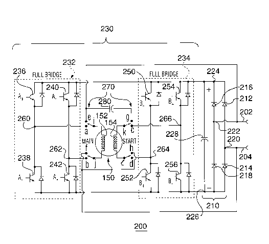
generating the two-phase power. Fig. 3 illustrstes an induction
motor drive system 200 constructed in accordance with an
! - 13 -
,
20S0~0
, embodiment of the invention. System 200 i~ preferably constructed
to drive motor 150 (Fig. 2). System 200 includes line terminals
202 and 204 for connection to a line conductor and a reference or
~neutral conductor, respectively, of a single-phase AC power
source. System 200 also includes a rectifier circuit 210 for
rectifying AC power received from the single-phase AC source
coupled to terminals 202 and 204. Rectifier circuit 210 inc udes
a first pair of diodes 212 and 214 connected in series with the
polarity shown and a ~econd pair of diode~ 216 and 218 connected
in series with the polarity shown and in parallel with the first
pair of diodes. A tap node 220 between diodes 212 and 214 is
connected to line terminal 204 and a tap node 222 between diodes
216 and 218 is connected to line terminal 202. Rectifier circuit
210 outputs a rectified DC voltage on a positive output terminal
224 and a negative output,terminal 226. A capacitor 228 is
coupled between output terminsls 224 and 226 to filter the output
of rectifier circuit 210.
Rectifier circuit 210 operates in a well known manner to
rectify the single-phase AC volt~ge applied to line terminals 202
and 204 and provide the rectified output on output terminals 224
and 226 with the pol~rity shown in Fig. 3. The magnitude of the
rectified output voltsge on output terminals 224 and 226 would be
appro~im~tely equ~l to the RMS single-phsse AC voltage multiplied
by ~2.
System 200 al~o includes an inverter circuit 230 consisting
of full bridge inverter circuits 232 and 234. Bridge inverter
circuit 232 includes first and second bridge legs, the first
- 14 -
20~04~0
bridge leg consisting of a first pair of power switching
devices 236 and 238 connected in series acros6 output terminals
224 and 226 of rectifier circuit 210. The second bridge leg of
bridge inverter circuit 232 consists of a second pair of power
switching devices 240 and 242 connected in series across output
;terminals 224 and 226. Bridge inverter circuit 234, configured
the same as bridge circuit 232, includes first and second bridge
legs, the first bridge leg consisting of a first pair of power
switching devices 250 and 252 connected in series across output
terminals 224 and 226. The second bridge leg of bridge inverter
circuit 234 consists of a second pair of power switching devices
254 and 256 also connected in series across output terminal~ 224
and 226.
Bridge inverter circuit 232 includes a tap node 260 between
switching devices 236 and 238 and a tap node 262 between switching
devices 240 and 242. Bridge inverter circuit 234 includes a tap
node 264 between switching devices 250 and 252 and a tap node 266
between switching devices 254 and 256.
Each of the power switching devices of bridge circuits 232
I and 234 can be provided as a transistor, insulated gate bipolar
! tran~istor, F.E.T., G.T.O. device or similar power switching
device connected with an accompanying anti-parallel conduction
diode, as shown in Fig. 3.
System 200 additionally includes a four-pole, double throw
switch 270 to enable operation of motor 150 in a single-phase mode
by connection to the single-phase source connected to line
terminals 202 and 204 or in a two-phase mode by connection to the
2060440
output of inverter circuit 230. Switch 270 includes pairs of
terminals a-b, c-d, e-f, g-h, i-; and k-l. The pair of terminals
a and b are respectively connected to tap nodes 260 and 262 of
bridge circuit 232. The pair of terminal~ c and d are
respectively connected to tap nodes 266 and 264 of bridge circuit
234. The pair of terminals e and f are respectively connected to
line terminals 202 and 204. With re~pect to the pair of terminals
g and h, terminal g is connected to line terminal 202 through a
run capacitor 280 and terminal h is connected directly to line
terminal 204. The pair of terminals i and j are respectively
connected to opposite ends of winding 152 of motor 150. The pair
of terminals k and 1 are respectively connected to opposite ends
of winding 154 of motor 150.
When switch 270 is in a first position connecting terminals a
and b to terminals i and ~, respectively, and terminals c and d to
terminals k and 1, respectively, motor 150 is operated in the
two-phase mode from the output of inverter circuit 230, as
described more fully below. When switch 270 is in a second
position connecting terminals e and f to ter~in~ls i and ~,
re~pectively, snd tQrminals g and h to terminsls k and 1,
respectively, motor 150 is operated in the single-phase mode from
the lngle-phase AC source. During the single-phase mode of
operation, run capacitor 280 iR connected in series between
winding 154 and line terminal 202. Since motor 150 is preferably
provided as a conventional PSC motor, capacitor 280 is preferably
20~0440
selected to have the run capacitor characteristics specified by
the m~nufacturer of motor 150, 80 that motor 150 operates as a
conventional PSC motor in the single-phase mode.
In accordance with the illustrated embodiment of the present
invention, in the two-phase operating mode, inverter circuit 230
is operated to convert the output of rectifier circuit 210 to a
two-phase pulse width modulated (PWM) output to drive motor 150.
In particular with respect to bridge circuit 232, switching
devices 236 and 242 are operated by a switch driving signal A+ and
switching devices 238 and 240 are operated by a switch driving
signal A-, so that a first phase PWM sinusoidal voltage VA
corresponding to first phase voltsge Vpl (Fig. 2) is generated
across tap nodes 260 and 262 for application to motor winding 152.
Similarly, with respect to bridge circuit 234, switching devices
250 and 256 are operated by a switch driving signal B- and
switching devices 252 and 254 are operated by a switch driving
signal 8+, 80 that a second phase PWM sinusoidal voltage VB
corresponding to second pha~e volt~ge Vp2 (Fig. 2) is generated
across tap nodes 264 and 266 for application to motor winding 154.
Thus, the switching devices of bridge circuits 232 and 234
are operated to generate the first and second phase sinusoidal PWM
voltage~ VA and VB of a two-phase voltage for ~pplication across
motor windings 152 and 154, respectively, with a desired phase
angle difference therebetween, e.g., 90. Also, as described
above with respect to phase voltages Vpl and Vp2, the first and
second phase voltages VA and VB are generated 80 that the
magnitude of the second phase voltage VB applied across winding
- 17 -
,
20~4~0
154 exceeds the msgnitude of the first phase voltage VA appliedacro~s winding 152, and the ratio of the magnitudes of the second
phase voltage to the first phase voltage, i.e., vB/vA is a
;predetermined value. Further, as described more fully below, the
switch driving signals, A+, A-, B+ and B- are generated in a
manner enabling variable speed operation of motor 150 while
maintaining the desired phase angle difference between voltages vA
and VB, maintaining the predetermined ratio between the respective
magnitudes of voltages VA and VB, i.e., VB/VA, and maintaining a
substantially constant volts/hertz ratio for each winding of motor
150.
Fig. 4 illustrates a block diagram of a control circuit 300
for generating switch driving signals A+, A-, B+ and B- to control
the operation of inverter circuit 230 as described above. Fig. 5
illustrates the waveforms of various signals occurring during
operation of control circuit 300.
Referring now to Fig. 4, circuit 300 includes a speed ramp
rate circuit 302 connected to receive an externally generated
speed control signal that represents a desired operating speed of
motor 150. The speed control signal may be derived by sensing
some pnrameter or characteristic of the ~ystem, in which motor 150
is incorporated, in order to automatically control the motor speed
, in re~ponse to that sensed information. Alternatively, the speed
control ~ignal m~y be varied by means of an appropriate manually
ad~ustable control, such a~ a potentiometer. Circuit 302 converts
the speed control signal into a DC voltage, in a normalized range
of 0 to 5 volts, on its output 304. The specific construction of
- 18 -
2~6~ 0
circuit 302 depends on the nature of the speed control signal.
,However, for example and without limitation, if the speed control
~ignal is provided as _ 0 to 5 VDC signal, then circuit 302 can be
provided as an R-C network configured as a low pass filter.
The DC voltage output of circuit 302 is applied to an input
of 8 voltage controlled oscillstor (VCO) 306 that provide~ on its
output 308 a square wave having a frequency proportional to the DC
~voltage applied to the input of VCO 306. For example, VCO 306
provides a square wave output that has a frequency of 0 Hz,
61.44 RHz and 122.88 RHz re~pectively corresponding to DC voltage
inputs of 0, 2.5 and 5 volts. VCO 306 can be provided as a model
no. AD654JN manufactured by Analog Devices, Inc. of Norwood,
Massachusett~.
Output 308 of VCO 306 is connected to an inverted clock input
of a twelve bit binary counter 310. Only eleven counter output
terminAls, Ql to Qll~ of counter 310 are used. Counter 310 can be
provided as a model no. MC74HC4040N manufsctured by Motorola, Inc.
of Phoenix, Arizona.
Circuit 300 al~o includes a 2K-by-8 bit EEPROM 320 connected
to recQive on its AddrQss inputs ADl to ADll the output of counter
310 provided on output termin_ls Ql to Qll EEPROM 320 has store~
ther-in a look-up t_ble contA~ing digital data values that define
sinu~oidal waveforms WDA and WDB respectively corresponding to th~
PWM sinusoid_l ph_se voltages VA and VB to be generated by
inverter circuit 230. ~n the illustrated embodiment, digitally
rQpresented waveforms WDA and WDB have a pha~e angle difference
therebetween of 90, corresponding to the desired phsse angle
-- 19 --
2~044l~
difference between fir~t and qecond phase voltsges vA and vB.
Also, the digital data stored in EEPROM 320 defines waveforms wDA
~and WDB to have the same magnitude. The manner by which voltage
VB is generated to have a greater magnitude than voltage VA is
described more fully below.
The digital data representative of each waveform WDA and WDB
is stored in EEPROM 320 in digitally weighted form broken into
1024 incremental pieces per sinusoidal cycle. The incremental
digital data elements representative of waveforms WDA and WDB are
alternately stored at succ~ssive address locations in EEPROM 320
so that succe~sive address values generated by counter 310 cause
EEPROM 320 to produce on its data outputs Dl to D8 digital data
respectively describing incremental pieces representative of
waveforms WDA and WDB. EEPROM 320 can be provided as a model
no. NMC27C16Q manufactured by National Semiconductor, Inc. of
Santa Clara, California.
Referring again to Fig. 4, the data outputs Dl to D8 f
EEPROM 320 are applied to a digital input of a multiplying dual
digital-to-analog converter (DAC) circuit 330. DAC circuit 330
includes a DAC select input 332 which i9 connected to receive the
Ql counter output of counter 310. DAC circuit 330 converts to
analog form the digital data it receives from EEPROM 320 and
provides the analog result on either of its output~ 334 or 336
depending on the bin~ry value applied to its DAC select input 332.
Since counter output Ql iB the least significant bit of the output
of counter 310, DAC circuit 330 provides each succe6sive analog
output, corresponding to each successive digital data input,
- 20 -
20~0~40
alternately on its outputs 334 and 336. In the illustratedembodiment, sinusoidal analog waveforms A and B, corresponding to
phase voltages VA and VB, are respectively provided on outputs 336
and 334.
Fig. 5 illustrates analog sinusoidal waveforms A and B
provided on outputs 336 and 334 of DAC circuit 330. In accordance
with the illustrated embodiment, the magnitude of analog waveform
B is greater than the magnitude of analog waveform A,
corresponding to the above described desired relative magnitudes
of phase voltages Vpl and Vp2, or of PWM phase voltages VA and VB.
The manner for achieving the magnitude difference between the
analog waveforms A and B is descrlbed below. Also, analog
waveforms A and B have the desired phase angle therebetween, which
is 90 in the illustrated embodiment.
DAC circuit 330 i8 further connected to receive voltage
scaling signals on VREF input~ 338 and 340 that respectively
correspond to outputs 336 and 334. In accordance with the
magnitude of each voltage scaling signal, DAC circuit 330, by
operation of its multiplying function, scales the m~gnitude of its
analog outputs in proportion to the corresponding voltage scaling
signals. In the illustrated embodiment, a first voltage scaling
sign~1, havlng a magnitude suitable for application to VREF input
340, i~ generated by a level converter circuit 342 that is
connected to receive the DC voltage provided on output 304 of
circuit 302. Circuit 342 i8 configured to generate the first
scaling signal as a DC voltage in proportion to the desired
operating speed of motor 150 80 that a predetermined constant
- 21 -
~9604~0
volts/hertz ratio can be maintained for the voltage applied towinding 154 of motor 150. As a result, for example, the analog
sinusoidal waveform voltage B output by DAC circuit 330 on output
334 has a peak-to-peak magnitude approximately ranging from 0
volts to 2.5 volts respectively corresponding to output voltages
on output 304 of circuit 302 ranging from 0 volts to 5 volts.
Circuit 342 can be provided as a resistive divider circuit.
The above noted difference in magnitudes between analog
waveforms A and B is accomplished in the present embodiment by
applying a second scaling signal, to the VREF input 338, that has
a smaller magnitude than the first scaling signal applied to vREF
input 340. A ~caling circuit 344 is connected to receive the
first scaling signal generated by level converter circuit 342.
Circuit 344 applies the first scaling signal to VREF input 340
without modification and also generates the second scaling signal,
from the first scaling sLgnal, for application to VREF input 338.
Circuit 344 generates the second scaling signal such that the
ratio of the first ~caling signal to the second scaling signal is
substantially equal to the above noted desired relative magnitudes
of the first and second phase voltages, i.e., Vp2/Vpl or VB/VA.
In accordance with one construction, scaling circuit 344 is
provided as a resistive divider circuit that suitably attenuate~
the fir~t scaling signal to provide the second scaling ~ignal. In
accordance with a second construction, scaling circuit 344 is
provided as an operational amplifier circuit configured to provide
- 22 -
2~S~'10
a gain of less than 1.0 so that the second scaling signal can be
genersted from the first ~caling signal while maintaining the
desired ratio therebetween.
Although, in accordance with the present embodiment, level
;converter circuit 342 generates the first scaling signal, the
invention is not so limited. Circuit 342 can be suitably
calibrated so that the scaling signal generated thereby serves as
the second scaling signal, corresponding to analog waveform A, for
application to VREF input 338. Then, scaling circuit 344 can be
provided as an operational amplifier circuit configured to provide
~a gain of greater than 1.0 80 that the first scaling signal can be
generated from the second scaling signal while maintaining the
decired ratio therebetween.
DAC circuit 330 can be provided as a model no. AD7528 CMOS
dual 8-bit buffered multiplying DAC manufactured by Analog
Devices, Inc. of Norwood, Massachu~etts. That model DAC has two
VREF inputs which respectively correspond to its two analog
outputs.
Still referring to Fig. 4, the analog waveform6 B and A
provided on outputs 334 and 336 of DAC circuit 330, respectively
corresponding to digital waveforms WDB AND WDA and to phase
voltago~ VB and VA, are applied through conventional analog buffer
circuit~ 350 and 352 to first input~ of comparator circuits 354
and 356. Circuit 300 additionally includes a triangular wave
generator 370 that generates a triangular waveform T on its
output 372. The generated triangular waveform T can, for example,
have a peak-to-peak magnitude that varies from 1.25 to 3.75 volts
- 23 -
2~6Q440
and a frequency in the range of approximately 900 Hz to 1100 Hz.
The frequency of the triangular waveform T determines the
frequency at which switching signals are generated for application
tO the power switching devices of inverter circuit 230.
Triangular wave generator 370 can be provided as a circuit
including an operational amplifier and a comparator, having a
construction well known in the art. With respect to circuit 300,
it is preferred that triangular waveform T have a peak-to-peak
magnitude of 2.5 volts and a frequency of 1000 Hz.
The triangular waveform T generated on output 372 of
gener~tor 370 is applied to a second input of each of
comparators 354 and 356. Fig. S illustrates triangular waveform T
superposed on each of waveforms A and B, as received by
comparator~ 356 and 354, respectively. Each of comparators 354
and 356 generate~ on its output either ~ high logic level voltage,
e.g., 5 volts, or a low logic level voltage, e.g., 0 volts,
according to whether the magnitude of the applied analog waveform
voltage A or B is respectively greater or less than the magnitude
of triangular waveform T. As a result, the output of each
comparator constitutes a pulse width modulsted waveform.
The pul~e width modulated waveforms output by compsrators 354
and 3S6 are respectively appliod to underlsp snd output driver
circuits 380 and 382. Circuit 380 is configured to generate two
identicsl ~witch driving signals B- that are electrically isolated
from each other and that each have substantislly the same form as
the pulse width modulAted waveform applied to circuit 380 and a
- 2~ -
~ 3 ~
voltage level sufficient to drive power switching devices 250 and
256 (Fig. 3). Circuit 380 also includes a logic inverter circuit
,for generating two identical isolated switch driving signals B+
that are esch the logical complement of wsveform B- and have a
voltage level sufficient to drive switching device 252 and 254
(Fig. 3). Circuit 380 further includes underlap circuitry to
insure that signals B+ and B- never cause the respective switching
devices to which they are applied to turn on at the same time,
thereby providing for a time delay between the logic level
turn-off command and the actual interruption of current by the
switching device.
Circuit 382 is configured in the same way as circuit 380 so
that circuit 382 provide6 two isolated switch driving signals A+,
for driving switching devices 236 and 242 and two isolated driving
~ignals A- for driving switching device~ 238 and 240. Fig. 5
illustrates switch driving signals A+, A-, B+ and B-.
In the operation of inverter circuit 230 and control
circuit 300, circuit 300 generates switch driving signals A+, A-,
~B+ and B- which are applied to drive the switching devices of
inverter circuit 230, such that a ~witch is driven closed when the
driving signal applied thereto assumes a positive logic value. As
ia re~ult of the pulse width modulated (PWM) closures of the
~witching devices, PWM sinusoidal phase voltage~ VA and VB are
applied to windings 152 and 154 of motor 150. For example, the
operation of switching devices 236, 238, 240 and 242 results in
generation across tap nodes 260 and 262 of the PWM sinusoidal
voltage VA that is applied across winding 152. Similarly, the
- 25 -
2~6~44~
operation of switching devices 250, 252, 254 and 256 results in
generation across tap nodes 264 and 266 of the PWM sinusoidal
voltage VB thst i8 applied scross winding 154. PWM voltages VA
and VB are illustrated in Fig. S. It is noted that the voltage
magnitudes of phase voltages VA and VB are a function of the
magnitude of the DC voltage provided by rectifier circuit 210.
In the operstion of motor drive system 200, the system is
operable in either the two-phase or single-phase mode according to
the position of switch 270, as described above. With respect to
the two-phsse mode and in accordance with the well known operation
of pulse width modulated inverter circuits, the PWM phase voltages
~VA and VB generated by inverter circuit 230 and applied to motor
150, closely simulate the sinu~oidal waveforms they correspond to.
The operating speed of motor 150 can be varied in response to the
speed control signal. During such variation, a constant volts/
hertz ratio is maintsined for the voltage spplied to each winding
152 and 154 of motor 150 by operation of the multiplying function
of DAC circuit 330 in accordance with the first snd second voltage
scaling signsls provided by level converter circuit 342 and
scaling circuit 344. Further, while the sbsolute magnitudes of
the voltages VA and VB applied to motor 150 are varied during
vari~ble speed operation, the ratio between those voltages, i.e.,
their relative magnitude~, is maintsined con~tant since the
relative values of the first and second scaling signals are
maintained constant, while the magnitudes of those signals are
varied in response to the speed control signal.
- 26 -
1.
~6~a
In the single-phase mode, motor lS0 is opersted directly from
the single-phsse AC source, connected to line terminals 202 and
204, a9 a conventional PSC motor. As a result, motor 150 remains
available for operation even when inverter circuit 230 is not
available to drive motor 150.
During starting of motor 150, assuming operation at full,
rated speed i8 desired, the speed control signal can initially
;require such full speed operation, which would result in an
initial application of full voltage across the motor windings.
This in turn would result in large motor inrush currents. It
would therefore be necessary to provide the switching devices of
inverter circuit 230 with ~ current r~ting sufficient to
accommodate such inrush currents. Alternstively, still assuming
that full speed operation is desired, and in accordance with known
inverter operating practices, the speed control signal could
initially be generated to require a low speed corresponding to the
rated slip of the motor, i.e., approximately 2-5% of rated speed,
so that no more than rated current flows initially. The motor
could then be accelerated to rated speed by steadily increasing
the magnitude of the speed control signal.
Fig. 6 illustrates a control circuit 400, constructed in
accordance with another embodiment of the invention, for
controlling the operation of inverter circuit 230 (Fig. 3).
Circuit 400 includes a sinusoidal wave generator 402 for
generating a sine wave voltage signal on an output 404 and a
! cosine wave voltage signal on an output 406. Generator 402
includes a speed control input 408 for receiving the motor speed
- 27 _
2 0 ~ 0
control ~ignal, ~uch as described with respect to circuit 300, for
varying the frequency of the generated sine and cosine waves in
accordance with a desired motor speed. Generator 402-can be
provided as a model no. 4423 signal generator manufactured by
Burr-Brown, Inc. of Tuscon, Arizona.
In order to maintain a constant volts/hertz ratio for the
voltage generated by inverter circuit 230 as the motor speed is
varied, the sinusoidal and co6inusoidal voltage signals produced
by generator 402 on outputs 404 and 406 are respectively passed
through high pass filters 410 and 412. High pa8s filters 410 and
412 comprise series connected capacitors 414 and 416, and shunt
connected resistors 418 and 420. Each high pass filter 410 and
412 has a 6dB/octsve roll-off characteristic and a cut-off
frequency above the upper limit of the operating frequency range
for motor 150. As a result, the sine and cosine wsve voltage
signals produced by generator 402 are respectively attenuated by
high pass filters 410 and 412 in an amount inversely proportional
to the frequency of the ~ine/cosine wave signals. The 6dB/octave
roll-off characteri6tic provides a lsl inverse relationship
between changes in frequency snd voltage. In this way, the
amplitude of the sine and cosine wave signals, at the outputs of
high pass filters 410 and 412, respectively, vary with and are
directly proportional to, frequency changes in generator 402,
thereby achievlng a constant volts/hertz ratio for esch filter
output. Exemplary characteristic~ of capacitors 414 and 416 and
resistors 418 and 420, corre~ponding to the above-noted high pass
- 28 -
20604~
filter characteristics, are 0.1 ~F for each of capacitors 414 and
416, and 10 Kn for each of resistors 418 and 420.
Still referring to Fig. 6, resistor 418 is preferably
provided as a potentiometer with an adjusting arm 422. Arm 422,
and hence the output of high pass filter 410, is connected to a
first input of a comparator circuit 430. The output of high pass
filter 412 is connected to a first input of a comparator circuit
432. Circuit 400 further includes a triangular wave generator 440
connected to apply its triangular wave signal output to respective
second inputs of both comparators 430 and 432. Generator 440 can
be the same as generator 370 described above with respect to
Fig. 4. Each comparator 430 and 432 generates on its output
either a high or a low logic level voltage according to whether
the magnitude of the applied sinusoidsl or cosinusoidal signal is
grsater or less than the magnitude of the applied triangular wave.
Thus, the comparison performed by each comparator 430 and 432 and
the resulting output is substantially the same as described above
with respect to comparators 354 and 356 and illustrated in Fig. 5,
i.e., each comparator generates a pulse width modulated control
signal.
The outputs of compsrators 430 and 432 are respectively
applied to underlap and output driver circuits 450 and 452 each of
which have substantially the same construction and function as
circuits 380 and 382 described above with respect to Fig. 4. As a
result, circuit 450 provides two isolated switch driving signals
A+ and two isolated driving ~ignals A- for driving the switching
devices of full bridge inverter circuit 232 (Fig. 3). Similarly,
_ 29 -
i
20~0~40
circuit 452 provides two isolated swLtch driving signals B+ andtwo i~olated driving signals B- for driving the switching devices
of full bridge inverter circuit 234 (Fig. 3). Switch driving
signals A+, A-, B+, and B- generated by control circuit 400 are
substantially identical to the switch driving signals generated by
control circuit 300 and illustrated in Fig. 4.
Provision of resistor 418 as a potentiometer allows
adjustment of a setpoint of filter 410 to enable a reduction of
the magnitude of the sine wave voltage signal, generated by
generator 402, relative to the cosine wave voltage signal. This
in turn results in generation of signals, by comparator 430 and
circuit 450, that cause inverter circuit 230 to generate a pulse
width modulated voltage, for application to main winding 152, that
has a smaller magnitude than the voltage generated for application
to winding 154. As a result, the above described feature of the
illustrated embodiments whereby Vp2>Vpl, is implemented.
Application of the switch driving signals generated by
circuit 400 to the switching devices of inverter circuit 230
results in generation of the above de~cribed PWM pha~e voltages VA
and VB, having the form illustrated in Fig. 4, for application to
motor 150.
While drive system 200 including control circuit 300 or 400
has been describQd as providing a 90 phase angle difference
durinq operation in the two-phase mode, the invention is not so
,limited. The phase angle generated under control of control
circuit 300 can be ad~usted by storing in EEPROM 320 digital data
for waveforms having a desired phaçe angle therebetween that is
- 30 -
~6~ Q
other than 90. Circuit 400 can be modified to 6ubstitute a
sinusoidal wave generator for generator 402 that generates two
sinusoidal waves that have any desired phase angle difference
between them. As described above, the phase angle between the
sinusoidal waves generated by generator 402, or a generator
substituted therefor, is the phase angle between the voltages
applied to the windings of motor 150.
While control circuit 300 has been described as including
scaling circuit 344 to generste first and second scaling signals
so that analog waveforms A and B have predetermined different
magnitudes, the invention is not so limited. Instead, in a
modification of the illustrated embodiment, digital data values
can be stored in EEPROM 320 that define sinusoidal waveforms WDA
and WDB having different magnitudes such that the ratio of
waveform magnitudes WDB/WDA i~ substantially equal to the desired
ratio of phase voltages V~/VA. Then, VREF inputs 338 and 340 are
tied together, scaling circuit 344 is eliminated and the first
scaling signal generated by a level converter circuit 342 is
applied directly to VREF inputs 338 and 340. As a result, analog
waveforms A and B are generated having relative magnitudes with
the desired ratio therebetween, while the respective magnitudes of
waveforms A snd B vary in accordance with the first scaling signal
which in turn varies in respon~e to the speed control signal.
Although in accordance with this modification of the illustrated
embodiment, waveforms WDA and WDB are defined to have different
magnitudes, the digital dsta would still define those two
waveforms to have the desired phsse angle therebetween.
- 31 -
206~4Q
While illustrated embodiments of the invention have been
described in which a constant volts/hertz ratio is maintained for
each winding of motor 150, the invention is not so limited. With
respect to certain motor driven loads, e.g., fans, the magnitude
of the load varies with rotational speed. For such loads it may
be more efficient to vary the volts/hertz ratio for each motor
winding as a predetermined function of rotational speed. With
respect to motor drive system 200 when operated under control of
control circuit 300 (Fig. 4~, such variation of the volts/hertz
ratio can be accomplished by modifying level converter circuit 342
to generate the scaling signal in accordance with the
predetermined function of rotational speed.
While the present invention overcomes the above described
problems experienced in the operation of HVAC systems, it will now
;be apparent to those skilled in the srt that the invention can be
practiced in other system applications to likewise realize the
advantages of the invention.
The foregoing description of preferred embodiments of the
invention has been presented for purposes of illustration and
description. It is not intended to be exhaustive or to limit the
invention to the precise form disclosed, and modifications and
variations are possible in light of the ~bove teachings or may be
acquired from practice of the invention. The embodiments were
chosen and described in order to explain the principles of the
invention and its practical application to enable one skilled in
the art to utilize the invention in various embodiments and with
- 32 -
20fi~4~
vasious modifications as are suited to the pArticular use
contemplated. It is intended that the scope of the invention be
defined by the claims appended hereto, and their equivalents.