Note: Descriptions are shown in the official language in which they were submitted.
2060462
.
,1
APPARATUS AND METHOD FOR TIMING DISTRIBUTION
OVER AN ASYNCHRONOUS RING
Technical Field
This invention relates to a co,ll.,llll~ication network having a plurality of
5 nodes, and more particularly to a technique for distributing timing synchronization
among selected nodes.
Back~round of the ~vention
Surprisingly, as com~u~el~ grow in both power and proliferation~ so too
does their need to borrow and share more data with other colllpu~el~. This need to
10 exchange greater amounts of information can no longer be fully satisfied by the
periodic data transfer between two conl~u~els but, rather, requires the ~imlllt;~neous
interconnection among a number of them, each having a particular specialization yet
drawing from the speci~li7~tion of the others. These inte~.;ollllections are known as
networks, and while they are limited in size and found in only corporate
15 environments today, vast global geodesic ne~wc,lks will connect millions of islands
of information tomorrow.
Co"-",l"-ication ~y~ems which allow data transfer over telephone lines
at a few hundred bits per second have been an integral part of conl~u~el systems for
the past few decades. Only recently have networks capable of handling several
20 million bits per second been widely available. Local area networks (LAN) havetypically offered between 100 Kb/s and 10 Mb/s among a few hundred stations, andhave been limited to a local area (a kilometer or so). One such network, Ethernet, is
synchronous and operates at 10 Mb/s. Because rapid information transfer is
indispensable in our highly competitive society, Ethernet is being superseded by a
25 higher capacity network known as the Fiber Distributed Data Interface (FDDI) which
transmits 100 Mb/s of data over each of two counter-rotating rings. FDDI can
tolerate a separation of up to 2 kilometers between stations, and support a total cable
distance of 100 kilometers around a ring with 500 station attachments. FDDI
possesses enough bandwidth to support up to 800 voice channels or perhaps 1-2
30 digitized video channels. One problem with voice or video traffic over FDDI,
however, is that the network and interface are asynchronous, thereby preventing
timing information from passing across the network boundaries. Although FDDI
uses a Timed Token Protocol to provide both synchronous and asynchronous service,
no technique has emerged as being clearly superior for clock synchronization at
35 various stations around the ring. Whereas packet switching is possible over an
206091~
_
asynchronous network, circuit switching requires a synchronous network and for that
reason a synchronous FDDI network (FDDI-II) has been proposed. Unfortunately,
FDDI and FDDI-II are incompatible, which is to say that a node adapted for FDDI-II
operation cannot be part of an FDDI ring.
In an asynchronous system, each link requires its own clock. This
means that each link is frequency- and phase-asynchronous vis-a-vis all other links
in the ring, and that timing information cannot be recovered from the bit stream.
Accordingly, the distribution of synchronous infc ~ ation, such as conventional
telephone conversations, on the FDDI system, has certain inherent problems. One
10 well-known solution for tr~n~mitting synchronous infollllation over an asynchronous
facility is the use of elastic storage registers to buffer the differences in the bit rate.
That is, data are written into a shift register at a first bit rate and read out of the shift
register at a second bit rate. When packet information is being tr~n~mitte~l, it makes
little difference whether the read and write rates are slightly dirrelellt because
15 packets are generally limited in size and the elastic storage registers can be made as
large as desired. However, when tr~n~mitting continuous synchronous data, the
elastic storage registers will overflow or underflow with the undesirable result that
tr~n~mitte-l information will either be lost (overflow condition), or that incorrect
information will be created (underflow condition).
U.S. Patent 4,866,704 was issued on September 12, 1989 and discloses a
fiber-optic voice/data network. This patent teaches a technique for synchronizing a
local clock by monitoring the average fill of an elastic storage register (receiving
buffer), speeding up the local clock when the average fill is increasing, and slowing
the clock when the average fill is decreasing so that overflow and underflow are25 prevented. While this technique is useful, it requires that synchronous data be
continuously present to m~int~in synchronization.
It is also known to distribute a reference timing signal over a separate
link to each node in a network, including a ring network. However, such a technique
requires the installation of a separate network just for timing - thus defeating the
30 structural simplicity of the ring and adding to its cost. It is therefore desirable to
improve upon the prior art systems for distributing timing information over an
asynchronous ring.
Summary of the Invention
In accordance with the invention, a ring network includes a master node
35 and one or more slave nodes where data enter and exit the network. Each of these
nodes includes a clock for supplying timing information to equipment at that node.
- 2 -
2060~6~
The master node measures the time delay encountclcd by data traversing the
network, and transmits this measurement to the slave node. At the slave node, a
similar measurement of time delay is made and colllparcd with the mea~ulcllRnt
tr~nsmitted by the master node. Differences between these two measurements are
5 used to adjust the frequency of the clock at the slave node.
In the illustrative embodiment of the invention, clock synchronization is
optionally and independently available to any node in the ring network. As a result,
the ring network simlllt~neously ~up,L)ul~ both synchronous and asynchronous data
traffic. Accordingly, the plilllaly reason for developing a synchronous FDDI
10 network (FDDI-II) no longer obtains.
Brief Description of the D. awill~
The features and capabilities of the present invention will be more fully
understood when reference is made to the detailed description and the drawing, of
which
FIG. 1 illustrates a ring network having counter-rotating rings and a
plurality of nodes, each serving different host system equipment;
FIG. 2 discloses e~luiplllent used at a particular node in accordance with
the invention;
FIG. 3 shows a data packet such as used in the Fiber Distributed Data
20 Interface (FDDI);
FIG. 4 illustrates the operation of a Media Access Controller at a node
when repeating a data packet to the network;
FIG. 5 illustrates the operation of the Media Access Controller at a node
when supplying an idle data packet to the network; and
FIG. 6 discloses, in block form, the details of clock recovery in
accordance with the invention.
Detailed Des~ )t;on
An emerging standard (ANSI X3T9.5) - better known as the Fiber
Distributed Data Tnt~ ce (FDDI) - defines a 100 Mb/s, time-token protocol. This
30 protocol is to be implemented on an asynchronous, fiber-optic network optimized for
1300 nanometer technology. Fiber-optic coll~ unication is best suited for point-to-
point tr~n~mi~sion and is present in two local area network (LAN) topologies, the
active hub star, and the ring. Active stars require extensive connections to wherever
the central hub is located and introduce a single failure point that can disable the
35 entire LAN. Single-ring networks are like chains which are vulnerable to failures at
any station. FDDI minimi7es this by using dual, counter-rotating rings. This
- 3 -
__ 20~0~
provides an alternate path if a station or a link fails, allowing data to be wrapped
back onto the secondary ring in the event of failure. The secondary ring may be only
a standby ring, or it may be used for concurrent tr~nsmi~sion thereby providing a 200
Mb/s network. Additional background illfc,~ ation regarding FDDI is contained in5 an article by Floyd E. Ross entitled: FDDI - a Tutorial, published in the IEEE Comlllullications Magazine, May 1986 - Vol. 24, No. 5 at pp. 10-17.
Referring now to FIG. 1, there is disclosed an example of an FDDI
network comprising plhll~y ring 10 and counter-rotating secondary ring 20. Nodesare illustratively positioned at locations around the network that may be separated by
10 large distances. Associated with each node is a host system that is available to users
at all other nodes via the fiber-optic ring. Together they form a network whose
combined resources are formidable and diverse. A generalized host system 100 is
shown connecting stations 101, 102 to the FDDI network via network interf~ce
(N/I) 200. In the discussion that follows, network interface 200 and host system 100
15 are designated as the "master node." In the present invention, the master node
distributes timing information to all of the other nodes. Accordingly, network
interface 200 is similar to the other network interfaces 300 in all respects except that
it supplies timing information to them. Network interface 200 receives a timing
signal over line 50 via host system 100. Any pair of nodes desiring to exchange
20 synchronous data with each other need to synchronize their clocks. This can be
accomplished by adjusting the clock frequency at one of the nodes to agree with the
other, or by adjusting the clock frequency of both of the nodes to agree with a
reference clock. Once synchronization is achieved, information such as digitizedvoice can be tr~n~mitted and received by a~r~liate equipment at these nodes.
Host system 100 can be any mainframe, wolh~alion, minicompulel or
peripheral to which a network interface is attached. Its role is to provide and receive
network data and perform some higher-level protocol functions which are not
handled by the associated stations. Examples of other host systems include, but are
not limited to, mainframe 110, PBX 120, and gateways 130, 140.
Stations 131, 132 are shown connected to gateway 130 by, for example,
a network 30 (e.g., IEEE-802.5 token ring). Stations 141, 142 are shown connected
to gateway 140 by, for example, a bus 40 (e.g., IEEE-802.3 Ethernet or IEEE-802.4
token bus). Stations 121, 122 are shown connected to PBX 120. Each of these nodes
connects to the fiber-optic ring by a network interface (N/I) 300 whose operation is
35 defined in detail by FDDI standards, but will be briefly discussed hereinafter.
20604~2
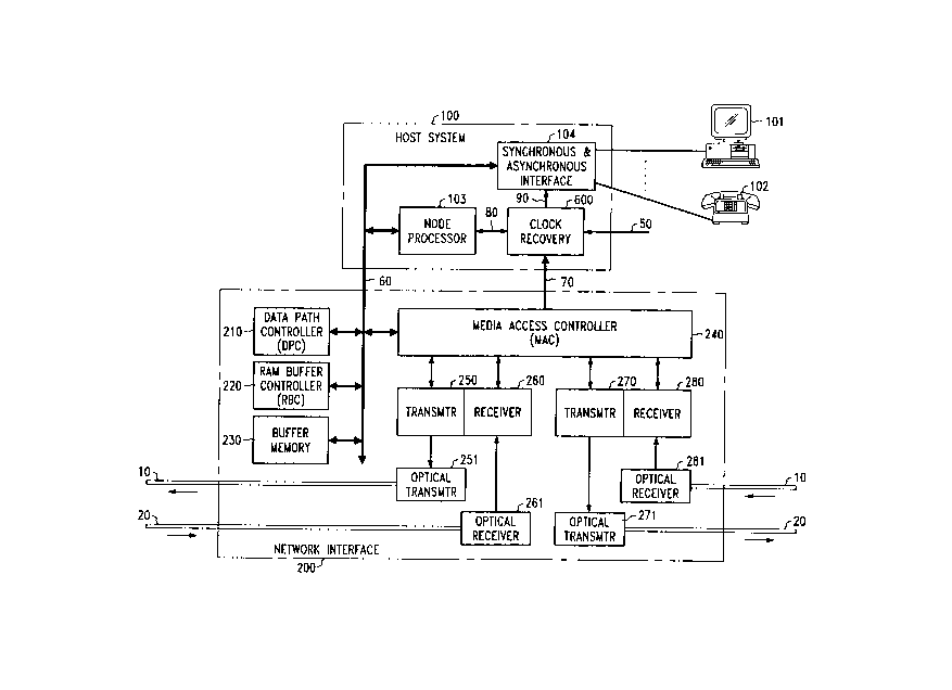
FIG. 2 discloses the eqllipm~nt needed at each node to support
interconnection with the FDDI network. Optical fibers 10, 20 are made from glass-
clad silica and consist of an inner core surrounded by a glass cladding (having a
(lirrelel~t refractive index than the silica) and a p~LecLi~/e sleeve. Plastic cladding is
S not used in FDDI applications because of its greater q~ttçnllq-tion. Optical
receivers 261, 281 receive modulated light-wave signals, whose center wavelengthlies between 1270 and 1380 nanometers, from optical fibers 20, 10 respectively, and
consist of a photodetector, an amplifier, a shaping filter, a compa-dtol, a buffer to
provide suitable electrical levels, and a signal detect circuit. The photodetector is
10 constructed from an InGaAs/InP PIN photodiode that senses light intensity andconverts it into current pulses. Optical tr~n~ 251, 271 transmit modulated
light-wave signals, whose wavelength~ are also in the 1300 nanometer range, to
optical fibers 10, 20 respectively. Each optical trqnsmi~pr consists of a driver and a
light emittin~ diode (~ Fn). The LED is typically made of InGaAsP, and generates15 light whose intensity is a function of the input data to be tr~n~mitteA
Tr~nsmitt~r/receiver pair 250, 260 controls the encoding and decoding
of data and control symbols, seriqli7ing the data clock recovery, line-state detection
and reporting. In operation, tr~ ,. 250 s~ri~li7es eight-bit-wide parallel data
from Media Access Controller (MAC) 240 to produce non-return-to-zero (NRZ)
20 code. 4B/SB coding is used which compri~es tr~n~lqtion of 4-bit groups of data into
a 5-bit value, and conversion into the NRZ format for trqn~mis~ion on the fiber-optic
ring. 4B/5B encoding is said to be 80% efficient since a 100 Mb/s data rate
trqn~l~tes into a 125 megabaud rate which is present on the fiber-optic ring.
Receiver 260 decodes the data received from the fiber-optic ring and converts it into
25 symbols that can be recognized by the MAC. Tasks of receiver 260 include retiming
the data to an int~rnql clock via a phase-locked loop and an elastic buffer, andconverting 5-bit code back into 4-bit code. Dir~cnLial Manchester coding is
frequently cc.lllpa~ed with 4B/5B coding and has the advantage of being rich in clock
information with a transition at eveIy bit, but the disadvantage of being only 50%
30 efficient. Suitable devices for the trqn~mitt.~r and receiver are the AM7985 and
AM7984, respectively, which are commercially available from Advanced Micro
Devices, Inc.* Tl~ 270 and receiver 280 are idrntir~l to ~ ,. 250 and
receiver 260, but are ~e~ir~ted to lirr~ optical fibers.
Bus 60 comprises several buses. It incllldes, for example, a 32-bit bus
35 used to interconnect buffer ln~ ul.~ 230 with other devices, while several 16-bit
buses are used between controllers 210, 220 and 240 and node processor 103.
* TrqllPrnqrk
r~ ~ 5 -
20~46~
Data Path Controller (DPC) 210 converts data in received packets from
byte-wide to 32-bit parallel word formats, performs parity checks and generates
packet and node status. A suitable device for the DPC is the AM79C82.
RAM Buffer Controller (RBC) 220 generates addresses to buffer
5 llleluoly 230 for received and tr~n~mitted packets. The RBC handles buffer
management and arbitrates direct ll~~ ly access coming from DPC 210, node
processor 103 and other host system a~p~us. A suitable device for the RBC is theAM79C81.
Buffer memory 230 is a conventional 256-kbyte static random access
10 memory which is readily available from a number of commercial sources. The
buffer memory is a storage area accessible by the controllers 210, 220, 240, the node
processor 103 and other host system equipment.
Media Access Controller (MAC) 240 controls the right to transmit data
to the network based on ca~lulillg a token according to a set of network rules,
15 recognizes addresses, controls ring recovery, and handles network and frame status.
A suitable device for the MAC is the AM79C83. The above devices designated 210,
220, 240, 250, 260 are all coll,.~ercially available from Advanced Micro Devices,
Inc. in what is known as the SUPERNETTM chip set which has been designed to
conform to the FDDI standard.
Node processor 103 is a separate microprogrammed or conventional
microprocessor-based system used for offloading the host and overseeing the
operation of the network interface 200. The node processor co~ icates with the
network interface over bus 60. A suitable device is the AM29000 RISC Processor,
also co~ ;ially available from Advanced Micro Devices, Inc., which includes a
25 number of embedded counters. One of these counters is used as counter 660 in
FIG. 6, and is shown functionally separated from the node processor for greater
clarity in explaining the invention.
Block 104 (Synchronous and Asynchronous Tnterf~ce) contains the
ci~ui~ly needed to buffer information between memory 230 and a synchronous Time
30 Division Multiplexed (TDM) bus. Here, terminal 101 and telephone 102 represent
the kinds of devices that might be connected to such a bus. Block 104 uses Direct
Memory Accessing to move data between memory 230 and another buffer memory
within block 104. In addition, block 104 contains the circuitry needed to move data
to and from bus 60 and the TDM bus. A source of synchronous timing is provided
35 to block 104 over line 90. Since the present invention is concerned with establishing
timing, such as present on line 90, rather than its use, further details regarding
block 104 are omitted for clarity.
- 6 -
~0~0~62
FDDl Protocol
Inro~ a~ion is tr~n~mitte-l on the FDDI ring as packets of data, each
having a maximum size of 9000 symbols (4 bits/symbol) and only one node may
transmit a data packet at a time. However, in order to avoid anarchy, a single token
5 is passed from node to node giving the token holder an exclusive right to transmit
data. FDDI protocol promotes fair an detelmillistic access to network resources for
all stations. This is done using a timer that measures the time between token
arrivals, a timer that controls how long a token can be held for tr~n~mi~sion~ and a
counter that indicates the number of times the token arrives later than expected. The
10 rules for data trAn~mi~sion on FDDI depend upon the type of data to be sent. For
tran~mi~sion of synchronous data, the rules are straigllLrolwald. The amount of
synchronous data that can be tr~n~mitted at a given token oppollu~ y is limited by
the bandwidth-allocation process which assures that if every station transmits its
m;lxi,~"~ allotment of synchronous data, the negotiated target token-rotation time
15 (I~I~T) will not be exceeded. The tr~n~mi~sion of asynchronous data is slightly
more complicated, since the m ~xi~ time allotted for tr~n~mi~ion is not constant.
Instead, a station can transmit asynchronous data until the unused bandwidth on the
ring is exh~nsted
MAC 240 controls the flow of data tr~ncmicsion on the ring, and
20 indicates when a data packet is tr~n~mitted as well as when it has returned from a
trip around the network. This feature is highly important in the practice of theinvention as will be pointed out later. FIG. 3 discloses the format of an FDDI
packet 310. Packets are preceded by a PREAMBLE having a minimllm of 16 "idle"
control symbols. Packets begin with a Start Delimiter (SD) composed from the J
25 and K control symbols of the 4B/5B code. This is followed by a 2-data-symbol
Frame Control (FC) field that identifies the type of packet. The Destination Address
(DA) identifies the intended recipient of the packet. Likewise, the Source Address
(SA) i-lentifies the packet's sender. Addresses can be either 26 or 48 bits in length.
The DA field can point to a single station, a group of stations, or all stations on the
30 ring. Following SA comes the variable length information field (INFO). A Frame
Check Sequence (FCS) field contains 4 bytes of data that are the result of a 32-bit
Autodin II cyclic redlln(l~ncy check polynomial. The FCS ensures the data integrity
of the FC, DA, SA, INFO, and FCS fields. Following the FCS field, an End
Delimiter (ED) formed with the "T" symbol is tr~n~mitted The Frame Status (FS)
35 field is used for symbols that determine whether the packet was received with error,
if the address was recognized, or whether the packet was copied. The ma~illlullllength of the packet (here 9000 symbols) is limited by the length of the elastic buffer
- 7 -
~060~2
and the worst-case frequency difference between the clocks at two nodes.
Referring now to FIG. 4, it will be seen that MAC 240 acts like a switch.
Normally the switch selects a source of IDLE control symbols for tr~n~mi~sion onthe ring. When the Start Delimiter arrives, MAC 240 switches to a repeat path. T he
S packet is monitored, copied if required, and sim-llt~neously repeated. MAC 240 can
also switch to source its own packets or issue a token. Packets are removed from the
ring by the originating station. This process, called "stripping", is illustrated in FIG.
5. The MAC repeats the packet until the SA field is received. Upon recognition of
the Source Address, the switch moves to the IDLE position. The resulting packet
10 fragment on the ring is ignored and eventually removed when it reaches a station
holding the token for tr~n~mi~ion. A station wishing to transmit must first
"capture" a token. The token is a 6-symbol packet that is uniquely recognized. Astation captures the token by performing the stripping action. Only the token SDfield is repeated on the ring. Once the token is captured, the station can begin15 tr~n~mitting packets. When the last packet is sent, the station immP(li~tely follows
by issuing a new token.
It is noted that FDDI is asynchronous, which means that the clock at
each of the various nodes is not synchronized with a common oscillator. Such
synchronization frequently comes at a very high price. It is important, however, that
20 each of the nodes be equipped to receive and transmit data at an agreed-upon rate,
and that data formats be established for efficient c~""~ ication. FDDI employs an
interesting solution to the ring clocking problem. The total ring, including all of its
stations and all of its links, must continue to have the same apparent bit length
during data tr~n~mi~ n. Otherwise, some bits would be lost or gained as a frame
25 was repeated around the ring. In the face of jitter, voltage, temperature, and aging
effects, such stability can only be realized through special provisions. At each node,
an elastic buffer is inserted between the receiver, which employs a variable
frequency clock to track the clock of the previous tr~n~mitting station, and a
tr~n~mitter, which runs on a fixed-frequency clock. The elastic buffer at each
30 station, is re-initialized during a preamble which precedes each frame or token. This
has the effect of increasing, or decreasing, the length of the preamble which isinitially tr~n~mitte~ as 16 or more symbols. The tr~n~mittPr clocks typically have
0.005% stability and the elastic buffer stores 10 bits of data. Accordingly, while
significant data can be tr~n~mitte~l without exceeding the limits of the elastic buffer,
35 practical trade-offs are made between the accuracy of the clock and the length of the
buffer.
2060462
FIG. 6 discloses detail regarding the construction of clock recovery
circuit 600 which is used at both master and slave nodes to provide a source of
timing on ~ine 90 to all e~lui~ nt at the node which it serves. Switch 625 is used
for sçlçc~ing b~L~ n operation as a master timing source (position 1), a free-running
S timing source (position 2), or a slave timing source (position 3). Because digital
voice co~ ic~tion e.luip~nt at telephone offices typically use 8 kHz as the
sampling frequency when carrying out analog-to-digital conversion, 8 kHz is the
information rate for synchronous co,llLuul~ications. Accordingly, voltage-controlled
crystal osc~ tor (VCO) 640 operates at a multiple (N) of the 8 kHz base frequency
10 so that it can be easily synchronized there~illl. In an illustrative embodiment,
VCO 640 opeldtes at 8.192 MHz, and N=1024. Synchl~l~izdLion is not required at
any node which operates asynchronously, although ~y~c~vnization requires very
little in the way of ~lition~l components. For example, in the plef~ d
embodiment of the invention counter 620 is actually part of node processor 103 (see
15 FIG. 2), and gate array 610 only adds a few gates to a larger gate array (not shown)
used for pelr~,lll~Lt-g a number of other tasks within the host system. In the Free-~un
Mode, (position 2 of switch 625) VCO 640 provides an 8.192 MHz c ystal-
controlled timing signal to all using e lui~nL VCOs are well-known devices that
are available from a number of vendors inr~ in~ CTS* Corporation and SaRonix*.
Syll~ ol~u~ g VCO 640 to an 8 kHz signal, such as provided by a
telephone office, is accomplished when switch 625 is in position 1 where operation as
the master source of timing for the ring network is desired. Divide-by-N counter 660
functions to divide the 8.192 MHz signal by 1024 to provide an 8 kHz square wavewhose phase is compared with the phase of a ,ere,e,lce 8 kHz signal on input line 50.
Phase c(~ a~Ol 650 is a conventional phase-locked-loop, such as the 74HC4046M,
which is a cu,lll"~.eially available device from a number of vendors inrl~ in~ Signetics*
and National S~,uicol~lu-;lor Corporation*. The output of
the phase colllp3-dLor is a measure of the error in the frequency of the VCO. This
error signal comprises a binary signal whose logic levels are used to
30 increase/decrease the frequency of VCO 640. Alternatively, a phase COl~dtOl-
having output states other binary voltages may be advantageously used in the present
invention. Indeed, the following paragraph discloses a Tri-State Latch 615 that
provides an output state that neither increases nor decreases the frequency of the
VCO. When the "A" and "B" inputs to the phase comparator are identical, the VCO
35 is at the desired frequency, although the output signal alternates between the two
logic levels. Low-Pass filter 630 is used to smooth such time-varying signals at the
input to V~O 640 so that an averaged voltage is presented to the VCO.
r,,, * Tr~ m~rk ~ 9 ~
`s..,
2~60~6~
.
Synchronizing VCO 640 to timing inrollllation supplied by a remote
source of timing is accomplished when switch 625 is in position 3 where operation
as a slave node is desired. The fi-n-l~m~.nt~l principle adapted for use in the present
invention is simply stated: independent observers measuring the identical
5 phenomenon should reach an identical result. If not, then the measuring apparatus is
modified until the results are identical. In the present invention, the phenomenon to
be measured is the time delay that a data signal encounters during a single triparound the ring network. Since the ring network is identical for all observers, then
they should all measure identical time delays - but they do not. And the reason that
10 they do not is because the clocks that are used to make the measurements are
~irr~,lG.". The present invention designates one observer (master node) to make the
"official" measurement of time delay around the ring (ring latency), and to
cc"-""l-"icate this mea~w~n~nl to all nodes. Any node seeking to become
synchronous with the master node makes its own measurement of ring latency,
15 colll~al~t;s it with the "official" measurement made by the master node, and adjusts its
clock so that its measurement of ring latency is identical with that of the master.
Returning now to FM. 6, adjustments to VCO 640 are made based on
dirÇ~rences in ring latency measw~lllen~s. At this time, switch 625 is in position 3
(Slave Mode). AND gate 611 responds to three input signals from line 70 to provide
20 a start pulse for counter 620. When a synchronous data packet leaves Media Access
Controller 240 (see FIG. 2), all three inputs to AND gate 611 are high causing its
output to also become high. Using the illustrative AM79C83 device, these leads are
designated RDYTBYT, XFRBYTE and XMEDAVS. It is noted that this
synchronous packet is generated by the node, and not a repeated synchronous packet!
25 Another signal line FSVLD*, also from MAC 240, signals when the node has
received its own packet - which is to say that the tr:ln~mitt~l packet has traversed the
entire ring and needs to be stripped from the ring. This signal (FSVLD*) is used to
stop counter 620 so that the number which is present at the output of the counter is
the number of cycles of the 8.192 MHz clock that have occurred between the start30 and stop pulses and is a measure of ring latency delivered to node processor 103 (see
FIG. 2) which appends this number to the end of the next synchronous packet that is
to be sent around the ring. This is done regardless of whether the node is the master
or a slave. If the node is the master, the process is ended. If the node is a slave, the
node processor compares the value that is read from counter 620 to the value that the
35 master node tr~n~mitted on its last synchronous packet. These values are subtracted
from each other in the node processor and the results of the subtraction are delivered
to latch 615. In the preferred embodiment of the invention, latch 615 provides three
- 10-
206Q~2
output states comprising +S volts, ground, or an open circuit. These states are used
to either increase, decrease, or not affect the frequency of the voltage-controlled
crystal oscillator 640.
Although a particular embodiment has been shown and described, it is
5 understood that various modifications are possible within the spirit and scope of the
invention. These modifications include, but are not limited to, use of the invention
on non fiber-optic ne~wc,lk~, ring latency measurements in which the data packetmakes more than a single excursion around the ring, use of the invention in a
network where packets, per-se, are not used, and use of the invention in
10 configurations where node connections are parallel rather than serial. Furthermore, it
is understood that in a network of counter-rotating rings, either ring may be used for
ring latency mea~urell~n~ and either ring may be used to transmit the results of such
mea~ llenLs. While it is pl~r~llc;d that the master and the slave nodes each use the
same ring to make latency measurements, it is not required.
- 11 -